JP2017120911A - 発光装置 - Google Patents
発光装置 Download PDFInfo
- Publication number
- JP2017120911A JP2017120911A JP2016256568A JP2016256568A JP2017120911A JP 2017120911 A JP2017120911 A JP 2017120911A JP 2016256568 A JP2016256568 A JP 2016256568A JP 2016256568 A JP2016256568 A JP 2016256568A JP 2017120911 A JP2017120911 A JP 2017120911A
- Authority
- JP
- Japan
- Prior art keywords
- light
- light emitting
- emitting device
- reflective layer
- layer
- Prior art date
- Legal status (The legal status is an assumption and is not a legal conclusion. Google has not performed a legal analysis and makes no representation as to the accuracy of the status listed.)
- Granted
Links
Images
















































Classifications
-
- H—ELECTRICITY
- H10—SEMICONDUCTOR DEVICES; ELECTRIC SOLID-STATE DEVICES NOT OTHERWISE PROVIDED FOR
- H10H—INORGANIC LIGHT-EMITTING SEMICONDUCTOR DEVICES HAVING POTENTIAL BARRIERS
- H10H20/00—Individual inorganic light-emitting semiconductor devices having potential barriers, e.g. light-emitting diodes [LED]
- H10H20/80—Constructional details
- H10H20/85—Packages
- H10H20/855—Optical field-shaping means, e.g. lenses
-
- H—ELECTRICITY
- H10—SEMICONDUCTOR DEVICES; ELECTRIC SOLID-STATE DEVICES NOT OTHERWISE PROVIDED FOR
- H10H—INORGANIC LIGHT-EMITTING SEMICONDUCTOR DEVICES HAVING POTENTIAL BARRIERS
- H10H20/00—Individual inorganic light-emitting semiconductor devices having potential barriers, e.g. light-emitting diodes [LED]
- H10H20/01—Manufacture or treatment
- H10H20/036—Manufacture or treatment of packages
- H10H20/0363—Manufacture or treatment of packages of optical field-shaping means
-
- H—ELECTRICITY
- H10—SEMICONDUCTOR DEVICES; ELECTRIC SOLID-STATE DEVICES NOT OTHERWISE PROVIDED FOR
- H10H—INORGANIC LIGHT-EMITTING SEMICONDUCTOR DEVICES HAVING POTENTIAL BARRIERS
- H10H20/00—Individual inorganic light-emitting semiconductor devices having potential barriers, e.g. light-emitting diodes [LED]
- H10H20/80—Constructional details
- H10H20/81—Bodies
- H10H20/814—Bodies having reflecting means, e.g. semiconductor Bragg reflectors
-
- H—ELECTRICITY
- H10—SEMICONDUCTOR DEVICES; ELECTRIC SOLID-STATE DEVICES NOT OTHERWISE PROVIDED FOR
- H10H—INORGANIC LIGHT-EMITTING SEMICONDUCTOR DEVICES HAVING POTENTIAL BARRIERS
- H10H20/00—Individual inorganic light-emitting semiconductor devices having potential barriers, e.g. light-emitting diodes [LED]
- H10H20/80—Constructional details
- H10H20/81—Bodies
- H10H20/819—Bodies characterised by their shape, e.g. curved or truncated substrates
-
- H—ELECTRICITY
- H10—SEMICONDUCTOR DEVICES; ELECTRIC SOLID-STATE DEVICES NOT OTHERWISE PROVIDED FOR
- H10H—INORGANIC LIGHT-EMITTING SEMICONDUCTOR DEVICES HAVING POTENTIAL BARRIERS
- H10H20/00—Individual inorganic light-emitting semiconductor devices having potential barriers, e.g. light-emitting diodes [LED]
- H10H20/80—Constructional details
- H10H20/83—Electrodes
- H10H20/831—Electrodes characterised by their shape
-
- H—ELECTRICITY
- H10—SEMICONDUCTOR DEVICES; ELECTRIC SOLID-STATE DEVICES NOT OTHERWISE PROVIDED FOR
- H10H—INORGANIC LIGHT-EMITTING SEMICONDUCTOR DEVICES HAVING POTENTIAL BARRIERS
- H10H20/00—Individual inorganic light-emitting semiconductor devices having potential barriers, e.g. light-emitting diodes [LED]
- H10H20/80—Constructional details
- H10H20/84—Coatings, e.g. passivation layers or antireflective coatings
-
- H—ELECTRICITY
- H10—SEMICONDUCTOR DEVICES; ELECTRIC SOLID-STATE DEVICES NOT OTHERWISE PROVIDED FOR
- H10H—INORGANIC LIGHT-EMITTING SEMICONDUCTOR DEVICES HAVING POTENTIAL BARRIERS
- H10H20/00—Individual inorganic light-emitting semiconductor devices having potential barriers, e.g. light-emitting diodes [LED]
- H10H20/80—Constructional details
- H10H20/85—Packages
- H10H20/851—Wavelength conversion means
- H10H20/8511—Wavelength conversion means characterised by their material, e.g. binder
- H10H20/8512—Wavelength conversion materials
- H10H20/8513—Wavelength conversion materials having two or more wavelength conversion materials
-
- H—ELECTRICITY
- H10—SEMICONDUCTOR DEVICES; ELECTRIC SOLID-STATE DEVICES NOT OTHERWISE PROVIDED FOR
- H10H—INORGANIC LIGHT-EMITTING SEMICONDUCTOR DEVICES HAVING POTENTIAL BARRIERS
- H10H20/00—Individual inorganic light-emitting semiconductor devices having potential barriers, e.g. light-emitting diodes [LED]
- H10H20/80—Constructional details
- H10H20/85—Packages
- H10H20/852—Encapsulations
- H10H20/853—Encapsulations characterised by their shape
-
- H—ELECTRICITY
- H10—SEMICONDUCTOR DEVICES; ELECTRIC SOLID-STATE DEVICES NOT OTHERWISE PROVIDED FOR
- H10H—INORGANIC LIGHT-EMITTING SEMICONDUCTOR DEVICES HAVING POTENTIAL BARRIERS
- H10H20/00—Individual inorganic light-emitting semiconductor devices having potential barriers, e.g. light-emitting diodes [LED]
- H10H20/80—Constructional details
- H10H20/85—Packages
- H10H20/855—Optical field-shaping means, e.g. lenses
- H10H20/856—Reflecting means
-
- H—ELECTRICITY
- H10—SEMICONDUCTOR DEVICES; ELECTRIC SOLID-STATE DEVICES NOT OTHERWISE PROVIDED FOR
- H10W—GENERIC PACKAGES, INTERCONNECTIONS, CONNECTORS OR OTHER CONSTRUCTIONAL DETAILS OF DEVICES COVERED BY CLASS H10
- H10W90/00—Package configurations
-
- G—PHYSICS
- G02—OPTICS
- G02B—OPTICAL ELEMENTS, SYSTEMS OR APPARATUS
- G02B6/00—Light guides; Structural details of arrangements comprising light guides and other optical elements, e.g. couplings
- G02B6/0001—Light guides; Structural details of arrangements comprising light guides and other optical elements, e.g. couplings specially adapted for lighting devices or systems
- G02B6/0011—Light guides; Structural details of arrangements comprising light guides and other optical elements, e.g. couplings specially adapted for lighting devices or systems the light guides being planar or of plate-like form
- G02B6/0066—Light guides; Structural details of arrangements comprising light guides and other optical elements, e.g. couplings specially adapted for lighting devices or systems the light guides being planar or of plate-like form characterised by the light source being coupled to the light guide
- G02B6/0068—Arrangements of plural sources, e.g. multi-colour light sources
-
- G—PHYSICS
- G02—OPTICS
- G02B—OPTICAL ELEMENTS, SYSTEMS OR APPARATUS
- G02B6/00—Light guides; Structural details of arrangements comprising light guides and other optical elements, e.g. couplings
- G02B6/0001—Light guides; Structural details of arrangements comprising light guides and other optical elements, e.g. couplings specially adapted for lighting devices or systems
- G02B6/0011—Light guides; Structural details of arrangements comprising light guides and other optical elements, e.g. couplings specially adapted for lighting devices or systems the light guides being planar or of plate-like form
- G02B6/0066—Light guides; Structural details of arrangements comprising light guides and other optical elements, e.g. couplings specially adapted for lighting devices or systems the light guides being planar or of plate-like form characterised by the light source being coupled to the light guide
- G02B6/0073—Light emitting diode [LED]
-
- H—ELECTRICITY
- H10—SEMICONDUCTOR DEVICES; ELECTRIC SOLID-STATE DEVICES NOT OTHERWISE PROVIDED FOR
- H10H—INORGANIC LIGHT-EMITTING SEMICONDUCTOR DEVICES HAVING POTENTIAL BARRIERS
- H10H20/00—Individual inorganic light-emitting semiconductor devices having potential barriers, e.g. light-emitting diodes [LED]
- H10H20/01—Manufacture or treatment
-
- H—ELECTRICITY
- H10—SEMICONDUCTOR DEVICES; ELECTRIC SOLID-STATE DEVICES NOT OTHERWISE PROVIDED FOR
- H10H—INORGANIC LIGHT-EMITTING SEMICONDUCTOR DEVICES HAVING POTENTIAL BARRIERS
- H10H20/00—Individual inorganic light-emitting semiconductor devices having potential barriers, e.g. light-emitting diodes [LED]
- H10H20/80—Constructional details
- H10H20/85—Packages
- H10H20/8506—Containers
-
- H—ELECTRICITY
- H10—SEMICONDUCTOR DEVICES; ELECTRIC SOLID-STATE DEVICES NOT OTHERWISE PROVIDED FOR
- H10H—INORGANIC LIGHT-EMITTING SEMICONDUCTOR DEVICES HAVING POTENTIAL BARRIERS
- H10H20/00—Individual inorganic light-emitting semiconductor devices having potential barriers, e.g. light-emitting diodes [LED]
- H10H20/80—Constructional details
- H10H20/85—Packages
- H10H20/852—Encapsulations
- H10H20/854—Encapsulations characterised by their material, e.g. epoxy or silicone resins
-
- H—ELECTRICITY
- H10—SEMICONDUCTOR DEVICES; ELECTRIC SOLID-STATE DEVICES NOT OTHERWISE PROVIDED FOR
- H10H—INORGANIC LIGHT-EMITTING SEMICONDUCTOR DEVICES HAVING POTENTIAL BARRIERS
- H10H20/00—Individual inorganic light-emitting semiconductor devices having potential barriers, e.g. light-emitting diodes [LED]
- H10H20/80—Constructional details
- H10H20/85—Packages
- H10H20/857—Interconnections, e.g. lead-frames, bond wires or solder balls
-
- H—ELECTRICITY
- H10—SEMICONDUCTOR DEVICES; ELECTRIC SOLID-STATE DEVICES NOT OTHERWISE PROVIDED FOR
- H10W—GENERIC PACKAGES, INTERCONNECTIONS, CONNECTORS OR OTHER CONSTRUCTIONAL DETAILS OF DEVICES COVERED BY CLASS H10
- H10W70/00—Package substrates; Interposers; Redistribution layers [RDL]
- H10W70/01—Manufacture or treatment
- H10W70/05—Manufacture or treatment of insulating or insulated package substrates, or of interposers, or of redistribution layers
- H10W70/08—Manufacture or treatment of insulating or insulated package substrates, or of interposers, or of redistribution layers by depositing layers on the chip or wafer, e.g. "chip-first" RDLs
- H10W70/09—Manufacture or treatment of insulating or insulated package substrates, or of interposers, or of redistribution layers by depositing layers on the chip or wafer, e.g. "chip-first" RDLs extending onto an encapsulation that laterally surrounds the chip or wafer, e.g. fan-out wafer level package [FOWLP] RDLs
-
- H—ELECTRICITY
- H10—SEMICONDUCTOR DEVICES; ELECTRIC SOLID-STATE DEVICES NOT OTHERWISE PROVIDED FOR
- H10W—GENERIC PACKAGES, INTERCONNECTIONS, CONNECTORS OR OTHER CONSTRUCTIONAL DETAILS OF DEVICES COVERED BY CLASS H10
- H10W74/00—Encapsulations, e.g. protective coatings
- H10W74/01—Manufacture or treatment
- H10W74/019—Manufacture or treatment using temporary auxiliary substrates
Landscapes
- Led Device Packages (AREA)
Abstract
Description

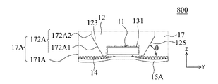
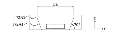
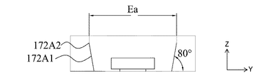
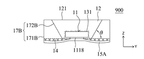
発光装置の高さが固定値である時に、斜面172A1の傾斜角度(θ)が小さいほど、発光装置の厚み(Y方向)が大きい。発光装置のサイズが大きくなるため、幾つかの分野に応用されにくくなる可能性がある。よって、斜面172A1の傾斜角度を設計する時に、その応用を考慮する必要があり、つまり、任意の角度でも良いとは言えない。
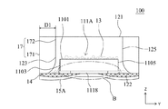
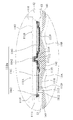
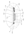
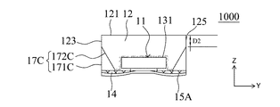
表2から分かるように、D3がD4よりも小さいとき、ΔDの絶対値が大きいほど、発光装置1100の発光角度が大きい。発光装置1100の発光角度は、透光体12を覆わない発光構造11の発光角度に接近することができる。第19図との相違点は、第22B及び第22C図では、斜面172Cの上方が透光体12により覆われ、且つ、第19図における平面172A2を含む部分を有しないことにある。第22B図に示すように、斜面172Cを含む部分が、発光構造11よりも大きい高さを有する時に、発光装置1000が発する光は、斜面172Cを経由して透光体12の上方へ反射されて、発光装置1000を離れることができる。発光構造11の発光角度(例えば、140度)は、斜面172Cにより、発光装置1000の発光角度を小さくさせることができる(例えば、120度)。一方、第22C図に示すように、斜面172Cが、発光構造11よりも小さい高さを有する時に、発光構造11が発する一部の光は、斜面172Cで反射されず、発光装置1100を直接離れるので、発光装置1100の発光角度は、発光装置1000の発光角度よりも大きいが、発光構造11の発光角度よりも小さい(例えば、120度よりも大きく、140度よりも小さい)。斜面のところの部分の高さの設計により、発光装置が異なる発光角度を有すようにさせることができ、これにより、発光装置の応用分野を広げることができる。
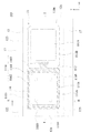
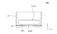
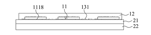
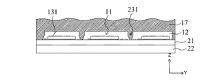
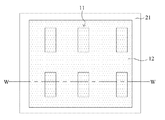
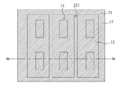
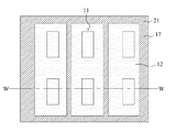
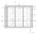
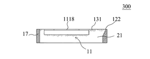
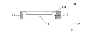
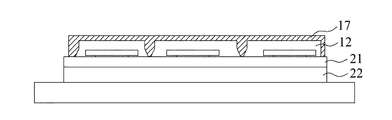
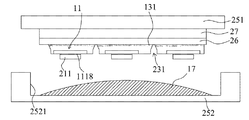
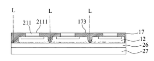
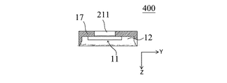
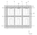
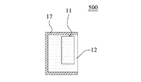
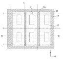
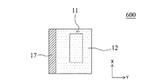
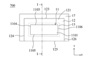
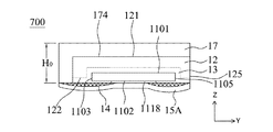
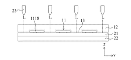
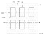
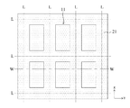
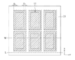
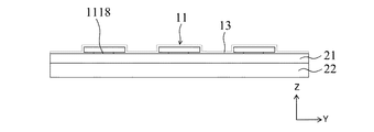
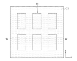
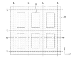
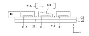
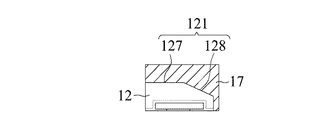
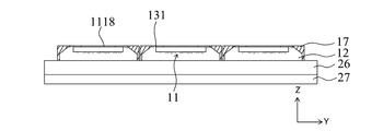
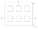
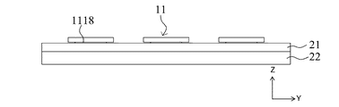
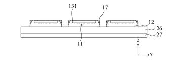
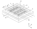
11、11D、11E、11F 発光構造
110 パターン化基板
1101 上表面
1102 下表面
103 第一側表面
1104 第二側表面
1105 第三側表面
1106 第四側表面
1110 孔
111A、111B 発光本体
1111 第一型半導体層
1112 活性層
1113 第二型半導体層
1114 第一絶縁層
1115 第二絶縁層
1116 導電層
1117 第三絶縁層
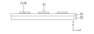
1118 第一電極
1119 第二電極
1120 オーム接触層
1161 第一領域
1162 第二領域
1163 第三領域
112 トレンチ
211 電極層
1124 上表面
12 透光体
121 上表面
122 下表面
123 第一側表面
124 第二側表面
125 第三側表面
126 第四側表面
13 波長変換体
131 波長変換粒子
14 第一反射層
15A、15B 延伸電極
151 第一端
152 第二端
17、17A、17B、17C 第二反射層
171、171’、171’’、171’’’、171A、171B、171C 外表面
172、172’、172’’、172’’’、172A、172B、172C 内表面
172A1 斜面
172A2 平面
173 上表面
174 下表面
21、26 接着材
22、27 載置板
23、23A、23B カッター
231 溝
251 上金型
252 下金型
2521、38 凹部
37 反射フレーム
371 スルー孔
901 発光源
9011 載置板
902 導光板
903 拡散板
904 反射器
Claims (10)
- 発光装置であって、
側表面を有する発光構造と
前記側表面を覆う反射層と、
を含み、
前記発光装置は、第一発光角度及び第二発光角度を有し、
前記第一発光角度と前記第二発光角度との差は、15度よりも大きい、発光装置。 - 請求項1に記載の発光装置であって、
前記発光構造を覆う透光体をさらに含む、発光装置。 - 請求項2に記載の発光装置であって、
前記透光体は、上表面、及び前記上表面に対向する下表面を含み、
前記発光装置は、前記下表面に位置する一対の延伸電極をさらに含む、発光装置。 - 請求項2項に記載の発光装置であって、
前記透光体は、第一側表面、第二側表面、第三側表面及び第四側表面を含み、
前記反射層は、前記第一側表面及び前記第三側表面を覆うが、前記第二側表面及び前記該第四側表面を覆わない、発光装置。 - 請求項4に記載の発光装置であって、
前記第一側表面は、前記第三側表面に対向し、
前記第二側表面は、前記第四側表面に対向する、発光装置。 - 請求項1に記載の発光装置であって、
前記第一発光角度は、130〜150度である、発光装置。 - 請求項1に記載の発光装置であって、
該第二発光角度は、100〜125度である、発光装置。 - 請求項1に記載の発光装置であって、
前記発光装置は、三つの出光面のみを含む、発光装置。 - 請求項1に記載の発光装置であって、
延伸電極を更に含み、
前記延伸電極と前記反射層とは、一方向において重なり合う、発光装置。 - 請求項1に記載の発光装置であって、
延伸電極を更に含み、
前記延伸電極及び前記反射層の側面は、ほぼ共平面である、発光装置。
Applications Claiming Priority (4)
| Application Number | Priority Date | Filing Date | Title |
|---|---|---|---|
| TW104144679 | 2015-12-31 | ||
| TW104144679 | 2015-12-31 | ||
| TW105126557 | 2016-08-19 | ||
| TW105126557 | 2016-08-19 |
Publications (3)
| Publication Number | Publication Date |
|---|---|
| JP2017120911A true JP2017120911A (ja) | 2017-07-06 |
| JP2017120911A5 JP2017120911A5 (ja) | 2020-02-20 |
| JP7266961B2 JP7266961B2 (ja) | 2023-05-01 |
Family
ID=57708468
Family Applications (1)
| Application Number | Title | Priority Date | Filing Date |
|---|---|---|---|
| JP2016256568A Active JP7266961B2 (ja) | 2015-12-31 | 2016-12-28 | 発光装置 |
Country Status (6)
| Country | Link |
|---|---|
| US (2) | US10205070B2 (ja) |
| EP (1) | EP3188263B1 (ja) |
| JP (1) | JP7266961B2 (ja) |
| KR (1) | KR102396074B1 (ja) |
| CN (2) | CN110649142B (ja) |
| TW (2) | TWI672547B (ja) |
Cited By (2)
| Publication number | Priority date | Publication date | Assignee | Title |
|---|---|---|---|---|
| KR20200006017A (ko) * | 2018-07-09 | 2020-01-17 | 니치아 카가쿠 고교 가부시키가이샤 | 발광 장치 및 그 제조 방법 |
| JP2022049000A (ja) * | 2020-09-15 | 2022-03-28 | 光森科技有限公司 | 光源モジュール |
Families Citing this family (16)
| Publication number | Priority date | Publication date | Assignee | Title |
|---|---|---|---|---|
| JP6665731B2 (ja) * | 2016-08-22 | 2020-03-13 | 豊田合成株式会社 | 発光装置及びその製造方法 |
| US10680147B2 (en) * | 2017-11-24 | 2020-06-09 | Osram Oled Gmbh | Method of producing a lighting device |
| WO2019106846A1 (ja) * | 2017-12-01 | 2019-06-06 | 日立化成株式会社 | 半導体装置の製造方法、仮固定材用樹脂組成物、及び仮固定材用積層フィルム |
| US11335842B2 (en) * | 2018-02-14 | 2022-05-17 | Maven Optronics Co., Ltd. | Chip-scale packaging light-emitting device with electrode polarity identifier and method of manufacturing the same |
| US10770636B2 (en) | 2018-02-14 | 2020-09-08 | Epistar Corporation | Light emitting device and manufacturing method thereof |
| TWD201606S (zh) * | 2018-06-28 | 2019-12-21 | 晶元光電股份有限公司 | 發光裝置 |
| TWD198613S (zh) | 2018-08-08 | 2019-07-11 | 晶元光電股份有限公司 | 發光二極體之部分 |
| CN112713166B (zh) * | 2019-10-25 | 2023-02-17 | 成都辰显光电有限公司 | 显示面板、电子设备及显示面板的制作方法 |
| CN113867044B (zh) * | 2020-06-30 | 2025-05-16 | 光森科技有限公司 | 光源模块 |
| TWI753573B (zh) * | 2020-06-30 | 2022-01-21 | 光森科技有限公司 | 光源模組 |
| US12344784B2 (en) * | 2020-08-31 | 2025-07-01 | Quantum Advanced Solutions Limited | Stabilized perovskite quantum dot material |
| TWD214986S (zh) * | 2020-10-07 | 2021-11-01 | 晶元光電股份有限公司 | 發光二極體之部分 |
| US11996384B2 (en) | 2020-12-15 | 2024-05-28 | Pulseforge, Inc. | Method and apparatus for debonding temporarily bonded wafers in wafer-level packaging applications |
| CN117099221A (zh) * | 2021-02-25 | 2023-11-21 | 艾迈斯-欧司朗国际有限责任公司 | 具有混合反射器的部件及其生产方法 |
| DE102021202920A1 (de) * | 2021-03-25 | 2022-09-29 | OSRAM Opto Semiconductors Gesellschaft mit beschränkter Haftung | Optoelektronischer halbleiterchip, herstellungsverfahren und halbleiterbauteil |
| KR102837821B1 (ko) * | 2022-05-24 | 2025-07-23 | 주식회사 루츠 | 형광체의 제조방법 |
Citations (8)
| Publication number | Priority date | Publication date | Assignee | Title |
|---|---|---|---|---|
| JP2004039778A (ja) * | 2002-07-02 | 2004-02-05 | Matsushita Electric Ind Co Ltd | 照明用発光素子 |
| JP2005072397A (ja) * | 2003-08-26 | 2005-03-17 | Kyocera Corp | 発光素子収納用パッケージおよび発光装置 |
| JP2010157638A (ja) * | 2008-12-27 | 2010-07-15 | Nichia Corp | 発光装置及びその製造方法 |
| WO2011093454A1 (ja) * | 2010-01-29 | 2011-08-04 | シチズン電子株式会社 | 発光装置の製造方法及び発光装置 |
| JP2013143496A (ja) * | 2012-01-11 | 2013-07-22 | Toshiba Corp | Ledパッケージ及びその製造方法 |
| KR20150030169A (ko) * | 2013-09-11 | 2015-03-19 | 엘지디스플레이 주식회사 | 발광 다이오드 소자 및 이를 포함하는 백라이트 유닛과 이의 제조 방법 |
| JP2015095658A (ja) * | 2013-11-14 | 2015-05-18 | 晶元光電股▲ふん▼有限公司 | 発光装置 |
| US20150221623A1 (en) * | 2014-02-05 | 2015-08-06 | Michael A. Tischler | Light-emitting dies incorporating wavelength-conversion materials and related methods |
Family Cites Families (44)
| Publication number | Priority date | Publication date | Assignee | Title |
|---|---|---|---|---|
| DE19714170C1 (de) * | 1997-03-21 | 1998-07-30 | Siemens Ag | Elektrooptisches Modul |
| JP2004127604A (ja) * | 2002-09-30 | 2004-04-22 | Citizen Electronics Co Ltd | 発光ダイオード及びバックライトユニット |
| JP4773048B2 (ja) * | 2003-09-30 | 2011-09-14 | シチズン電子株式会社 | 発光ダイオード |
| JP4330476B2 (ja) * | 2004-03-29 | 2009-09-16 | スタンレー電気株式会社 | 半導体発光素子 |
| KR20060077801A (ko) * | 2004-12-31 | 2006-07-05 | 엘지전자 주식회사 | 고출력 발광 다이오드 및 그의 제조 방법 |
| JP2006253298A (ja) * | 2005-03-09 | 2006-09-21 | Toshiba Corp | 半導体発光素子及び半導体発光装置 |
| JP2007165696A (ja) * | 2005-12-15 | 2007-06-28 | Sanyo Electric Co Ltd | 半導体装置及びその製造方法 |
| TWM304049U (en) * | 2006-07-19 | 2007-01-01 | K Bridge Electronics Co Ltd | Light source of backlight module |
| US8128261B2 (en) | 2006-08-25 | 2012-03-06 | Sharp Kabushiki Kaisha | Light emitting element, light emitting element array, backlight unit, and liquid crystal display |
| TW200834954A (en) | 2007-02-02 | 2008-08-16 | Lighthouse Technology Co Ltd | Light-emitting diode and backlight module comprising the same |
| JP5315070B2 (ja) * | 2008-02-07 | 2013-10-16 | 昭和電工株式会社 | 化合物半導体発光ダイオード |
| KR100972979B1 (ko) * | 2008-03-17 | 2010-07-29 | 삼성엘이디 주식회사 | 엘이디 패키지 및 그 제조방법 |
| US7800125B2 (en) * | 2008-07-09 | 2010-09-21 | Himax Display, Inc. | Light-emitting diode package |
| KR101332794B1 (ko) * | 2008-08-05 | 2013-11-25 | 삼성전자주식회사 | 발광 장치, 이를 포함하는 발광 시스템, 상기 발광 장치 및발광 시스템의 제조 방법 |
| KR101639793B1 (ko) * | 2008-09-25 | 2016-07-15 | 코닌클리케 필립스 엔.브이. | 코팅된 발광 장치 및 그 코팅 방법 |
| KR101497953B1 (ko) * | 2008-10-01 | 2015-03-05 | 삼성전자 주식회사 | 광추출 효율이 향상된 발광 소자, 이를 포함하는 발광 장치, 상기 발광 소자 및 발광 장치의 제조 방법 |
| JP5075786B2 (ja) * | 2008-10-06 | 2012-11-21 | 株式会社東芝 | 発光装置及びその製造方法 |
| WO2010044023A1 (en) * | 2008-10-17 | 2010-04-22 | Koninklijke Philips Electronics N.V. | Light emitting device |
| CN201289864Y (zh) * | 2008-11-19 | 2009-08-12 | 深圳市聚飞光电有限公司 | 侧面发光二极管 |
| JP2011061056A (ja) | 2009-09-11 | 2011-03-24 | Stanley Electric Co Ltd | 線状発光装置、その製造方法並びに面光源装置 |
| TW201120486A (en) * | 2009-12-14 | 2011-06-16 | Coretronic Corp | Brightness enhancement film and backlight module |
| KR100986560B1 (ko) * | 2010-02-11 | 2010-10-07 | 엘지이노텍 주식회사 | 발광소자 및 그 제조방법 |
| CN101872824A (zh) * | 2010-06-07 | 2010-10-27 | 厦门市三安光电科技有限公司 | 侧面具有双反射层的氮化镓基倒装发光二极管及其制备方法 |
| WO2012008220A1 (ja) * | 2010-07-12 | 2012-01-19 | シャープ株式会社 | 面発光装置および表示装置 |
| TWI423098B (zh) * | 2010-07-15 | 2014-01-11 | Quanta Comp Inc | 光學觸控結構 |
| US9134595B2 (en) * | 2011-09-29 | 2015-09-15 | Casio Computer Co., Ltd. | Phosphor device, illumination apparatus and projector apparatus |
| TW201318221A (zh) * | 2011-10-26 | 2013-05-01 | 漢磊科技股份有限公司 | 發光二極體之矽支架及其製造方法 |
| JP2013115088A (ja) | 2011-11-25 | 2013-06-10 | Citizen Holdings Co Ltd | 半導体発光装置 |
| JP2013157523A (ja) * | 2012-01-31 | 2013-08-15 | Toyoda Gosei Co Ltd | 半導体発光素子、半導体発光素子の製造方法および発光装置 |
| EP2815437B1 (en) * | 2012-02-16 | 2019-08-14 | Citizen Electronics Co., Ltd. | Light-emitting diode and method of manufacturing a light-emitting diode |
| JP5953155B2 (ja) * | 2012-02-24 | 2016-07-20 | スタンレー電気株式会社 | 半導体発光装置 |
| CN103515506B (zh) * | 2012-06-15 | 2017-04-26 | 展晶科技(深圳)有限公司 | 发光二极管封装结构及其制造方法 |
| JP5891133B2 (ja) * | 2012-07-12 | 2016-03-22 | スタンレー電気株式会社 | 半導体発光装置 |
| TWM461760U (zh) * | 2013-04-29 | 2013-09-11 | 勝華科技股份有限公司 | 光學透鏡與光源裝置 |
| CN103280508B (zh) * | 2013-05-24 | 2015-12-23 | 江阴长电先进封装有限公司 | 一种晶圆级led封装方法 |
| JP2015028984A (ja) * | 2013-07-30 | 2015-02-12 | 日亜化学工業株式会社 | 半導体発光素子 |
| JP6215612B2 (ja) * | 2013-08-07 | 2017-10-18 | ソニーセミコンダクタソリューションズ株式会社 | 発光素子、発光素子ウェーハ及び電子機器 |
| EP2854186A1 (en) | 2013-09-26 | 2015-04-01 | Seoul Semiconductor Co., Ltd. | Light source module, fabrication method therefor, and backlight unit including the same |
| TWI520383B (zh) * | 2013-10-14 | 2016-02-01 | 新世紀光電股份有限公司 | 發光二極體封裝結構 |
| JP6299176B2 (ja) | 2013-11-22 | 2018-03-28 | 日亜化学工業株式会社 | 発光装置およびその製造方法ならびにこの発光装置を備える照明装置 |
| CN103618041B (zh) * | 2013-12-11 | 2016-03-30 | 江阴长电先进封装有限公司 | 一种esd保护的led封装结构及其封装方法 |
| CN110265530B (zh) * | 2014-01-29 | 2023-03-21 | 亮锐控股有限公司 | 填充有密封剂的用于磷光体转换led的浅反射器杯 |
| US9608168B2 (en) * | 2014-06-13 | 2017-03-28 | Seoul Viosys Co., Ltd. | Light emitting diode |
| US10217904B2 (en) | 2015-02-03 | 2019-02-26 | Epistar Corporation | Light-emitting device with metallized mounting support structure |
-
2016
- 2016-12-28 JP JP2016256568A patent/JP7266961B2/ja active Active
- 2016-12-30 US US15/394,951 patent/US10205070B2/en active Active
- 2016-12-30 EP EP16207621.0A patent/EP3188263B1/en active Active
- 2016-12-30 TW TW105144197A patent/TWI672547B/zh active
- 2016-12-30 CN CN201910909540.4A patent/CN110649142B/zh active Active
- 2016-12-30 KR KR1020160184194A patent/KR102396074B1/ko active Active
- 2016-12-30 CN CN201611269825.9A patent/CN106960901B/zh active Active
- 2016-12-30 TW TW108129560A patent/TWI731394B/zh active
-
2018
- 2018-12-27 US US16/234,066 patent/US10586902B2/en active Active
Patent Citations (8)
| Publication number | Priority date | Publication date | Assignee | Title |
|---|---|---|---|---|
| JP2004039778A (ja) * | 2002-07-02 | 2004-02-05 | Matsushita Electric Ind Co Ltd | 照明用発光素子 |
| JP2005072397A (ja) * | 2003-08-26 | 2005-03-17 | Kyocera Corp | 発光素子収納用パッケージおよび発光装置 |
| JP2010157638A (ja) * | 2008-12-27 | 2010-07-15 | Nichia Corp | 発光装置及びその製造方法 |
| WO2011093454A1 (ja) * | 2010-01-29 | 2011-08-04 | シチズン電子株式会社 | 発光装置の製造方法及び発光装置 |
| JP2013143496A (ja) * | 2012-01-11 | 2013-07-22 | Toshiba Corp | Ledパッケージ及びその製造方法 |
| KR20150030169A (ko) * | 2013-09-11 | 2015-03-19 | 엘지디스플레이 주식회사 | 발광 다이오드 소자 및 이를 포함하는 백라이트 유닛과 이의 제조 방법 |
| JP2015095658A (ja) * | 2013-11-14 | 2015-05-18 | 晶元光電股▲ふん▼有限公司 | 発光装置 |
| US20150221623A1 (en) * | 2014-02-05 | 2015-08-06 | Michael A. Tischler | Light-emitting dies incorporating wavelength-conversion materials and related methods |
Cited By (6)
| Publication number | Priority date | Publication date | Assignee | Title |
|---|---|---|---|---|
| KR20200006017A (ko) * | 2018-07-09 | 2020-01-17 | 니치아 카가쿠 고교 가부시키가이샤 | 발광 장치 및 그 제조 방법 |
| JP2020013986A (ja) * | 2018-07-09 | 2020-01-23 | 日亜化学工業株式会社 | 発光装置及びその製造方法 |
| JP7348478B2 (ja) | 2018-07-09 | 2023-09-21 | 日亜化学工業株式会社 | 発光装置及びその製造方法 |
| KR102780286B1 (ko) * | 2018-07-09 | 2025-03-12 | 니치아 카가쿠 고교 가부시키가이샤 | 발광 장치 및 그 제조 방법 |
| JP2022049000A (ja) * | 2020-09-15 | 2022-03-28 | 光森科技有限公司 | 光源モジュール |
| JP7324255B2 (ja) | 2020-09-15 | 2023-08-09 | 光森科技有限公司 | 光源モジュール |
Also Published As
| Publication number | Publication date |
|---|---|
| US20190172987A1 (en) | 2019-06-06 |
| CN110649142A (zh) | 2020-01-03 |
| CN106960901A (zh) | 2017-07-18 |
| CN110649142B (zh) | 2024-01-16 |
| EP3188263A1 (en) | 2017-07-05 |
| KR20170080531A (ko) | 2017-07-10 |
| US20170194540A1 (en) | 2017-07-06 |
| TWI672547B (zh) | 2019-09-21 |
| CN106960901B (zh) | 2021-10-15 |
| EP3188263B1 (en) | 2024-04-03 |
| TWI731394B (zh) | 2021-06-21 |
| KR102396074B1 (ko) | 2022-05-09 |
| US10586902B2 (en) | 2020-03-10 |
| TW201727337A (zh) | 2017-08-01 |
| TW201944146A (zh) | 2019-11-16 |
| JP7266961B2 (ja) | 2023-05-01 |
| US10205070B2 (en) | 2019-02-12 |
Similar Documents
| Publication | Publication Date | Title |
|---|---|---|
| JP7266961B2 (ja) | 発光装置 | |
| US10804444B2 (en) | Light-emitting device and manufacturing method thereof | |
| CN107039573B (zh) | 发光元件及其制造方法 | |
| CN108133997B (zh) | 发光装置 | |
| US11165223B2 (en) | Semiconductor light source | |
| JP7295437B2 (ja) | 発光装置 | |
| JP2011507287A (ja) | 照明装置 | |
| JP2016518029A (ja) | 発光ダイオードコンポーネント | |
| TW201314973A (zh) | 光電組件及用於製造光電組件之方法 | |
| TWI829671B (zh) | 發光裝置 | |
| TW201639199A (zh) | 發光裝置 | |
| CN115347015A (zh) | 一种发光元件及显示装置 | |
| JP7583268B2 (ja) | 発光装置、発光モジュール、面状光源、液晶表示装置 | |
| CN207134382U (zh) | 发光装置、背光单元及液晶显示器 | |
| JP2022129961A (ja) | 発光装置および面状光源 | |
| US20210202795A1 (en) | Light-emitting module and method of manufacturing light-emitting module | |
| WO2023189384A1 (ja) | 発光デバイスおよび画像表示装置 | |
| JP2025538122A (ja) | パターン化された光変性層を含むサポート構造を有する発光ダイオードデバイス | |
| JP2022099119A (ja) | 発光装置および面状光源 | |
| JP2023001818A (ja) | 発光装置、発光モジュール、画像表示装置 |
Legal Events
| Date | Code | Title | Description |
|---|---|---|---|
| A521 | Request for written amendment filed |
Free format text: JAPANESE INTERMEDIATE CODE: A523 Effective date: 20191226 |
|
| A621 | Written request for application examination |
Free format text: JAPANESE INTERMEDIATE CODE: A621 Effective date: 20191226 |
|
| A977 | Report on retrieval |
Free format text: JAPANESE INTERMEDIATE CODE: A971007 Effective date: 20201210 |
|
| A131 | Notification of reasons for refusal |
Free format text: JAPANESE INTERMEDIATE CODE: A131 Effective date: 20210105 |
|
| A521 | Request for written amendment filed |
Free format text: JAPANESE INTERMEDIATE CODE: A523 Effective date: 20210331 |
|
| A131 | Notification of reasons for refusal |
Free format text: JAPANESE INTERMEDIATE CODE: A131 Effective date: 20210810 |
|
| A521 | Request for written amendment filed |
Free format text: JAPANESE INTERMEDIATE CODE: A523 Effective date: 20211108 |
|
| A131 | Notification of reasons for refusal |
Free format text: JAPANESE INTERMEDIATE CODE: A131 Effective date: 20220308 |
|
| A521 | Request for written amendment filed |
Free format text: JAPANESE INTERMEDIATE CODE: A523 Effective date: 20220602 |
|
| A131 | Notification of reasons for refusal |
Free format text: JAPANESE INTERMEDIATE CODE: A131 Effective date: 20220913 |
|
| A521 | Request for written amendment filed |
Free format text: JAPANESE INTERMEDIATE CODE: A523 Effective date: 20221209 |
|
| A131 | Notification of reasons for refusal |
Free format text: JAPANESE INTERMEDIATE CODE: A131 Effective date: 20221220 |
|
| A521 | Request for written amendment filed |
Free format text: JAPANESE INTERMEDIATE CODE: A523 Effective date: 20230313 |
|
| TRDD | Decision of grant or rejection written | ||
| A01 | Written decision to grant a patent or to grant a registration (utility model) |
Free format text: JAPANESE INTERMEDIATE CODE: A01 Effective date: 20230322 |
|
| A61 | First payment of annual fees (during grant procedure) |
Free format text: JAPANESE INTERMEDIATE CODE: A61 Effective date: 20230419 |
|
| R150 | Certificate of patent or registration of utility model |
Ref document number: 7266961 Country of ref document: JP Free format text: JAPANESE INTERMEDIATE CODE: R150 |
|
| S531 | Written request for registration of change of domicile |
Free format text: JAPANESE INTERMEDIATE CODE: R313531 |
|
| S533 | Written request for registration of change of name |
Free format text: JAPANESE INTERMEDIATE CODE: R313533 |
|
| R250 | Receipt of annual fees |
Free format text: JAPANESE INTERMEDIATE CODE: R250 |