JP2017128045A - 露光装置、画像形成ユニットおよび画像形成装置 - Google Patents
露光装置、画像形成ユニットおよび画像形成装置 Download PDFInfo
- Publication number
- JP2017128045A JP2017128045A JP2016009216A JP2016009216A JP2017128045A JP 2017128045 A JP2017128045 A JP 2017128045A JP 2016009216 A JP2016009216 A JP 2016009216A JP 2016009216 A JP2016009216 A JP 2016009216A JP 2017128045 A JP2017128045 A JP 2017128045A
- Authority
- JP
- Japan
- Prior art keywords
- image
- image forming
- light
- exposure intensity
- lens array
- Prior art date
- Legal status (The legal status is an assumption and is not a legal conclusion. Google has not performed a legal analysis and makes no representation as to the accuracy of the status listed.)
- Pending
Links
- 230000015572 biosynthetic process Effects 0.000 title description 12
- 230000014509 gene expression Effects 0.000 claims abstract description 4
- 238000009826 distribution Methods 0.000 claims description 25
- 238000003384 imaging method Methods 0.000 claims 1
- 230000003287 optical effect Effects 0.000 description 86
- 206010034972 Photosensitivity reaction Diseases 0.000 description 12
- 239000010410 layer Substances 0.000 description 12
- 230000036211 photosensitivity Effects 0.000 description 12
- 230000008859 change Effects 0.000 description 9
- 230000002093 peripheral effect Effects 0.000 description 8
- 238000000034 method Methods 0.000 description 7
- 230000008569 process Effects 0.000 description 7
- 238000004140 cleaning Methods 0.000 description 6
- 239000003086 colorant Substances 0.000 description 6
- 239000003795 chemical substances by application Substances 0.000 description 4
- 230000007423 decrease Effects 0.000 description 4
- 238000010586 diagram Methods 0.000 description 4
- 229910052751 metal Inorganic materials 0.000 description 4
- 239000002184 metal Substances 0.000 description 4
- 239000000758 substrate Substances 0.000 description 4
- 239000000463 material Substances 0.000 description 3
- 239000002344 surface layer Substances 0.000 description 3
- VYPSYNLAJGMNEJ-UHFFFAOYSA-N Silicium dioxide Chemical compound O=[Si]=O VYPSYNLAJGMNEJ-UHFFFAOYSA-N 0.000 description 2
- 230000009471 action Effects 0.000 description 2
- 239000000654 additive Substances 0.000 description 2
- 230000000996 additive effect Effects 0.000 description 2
- 229920001971 elastomer Polymers 0.000 description 2
- 230000031700 light absorption Effects 0.000 description 2
- 238000012986 modification Methods 0.000 description 2
- 230000004048 modification Effects 0.000 description 2
- 239000000049 pigment Substances 0.000 description 2
- 238000011144 upstream manufacturing Methods 0.000 description 2
- GWEVSGVZZGPLCZ-UHFFFAOYSA-N Titan oxide Chemical compound O=[Ti]=O GWEVSGVZZGPLCZ-UHFFFAOYSA-N 0.000 description 1
- 229920006311 Urethane elastomer Polymers 0.000 description 1
- 239000000853 adhesive Substances 0.000 description 1
- 230000001070 adhesive effect Effects 0.000 description 1
- 229910052782 aluminium Inorganic materials 0.000 description 1
- XAGFODPZIPBFFR-UHFFFAOYSA-N aluminium Chemical compound [Al] XAGFODPZIPBFFR-UHFFFAOYSA-N 0.000 description 1
- 239000011230 binding agent Substances 0.000 description 1
- 230000007547 defect Effects 0.000 description 1
- 238000007599 discharging Methods 0.000 description 1
- 230000000694 effects Effects 0.000 description 1
- 230000005684 electric field Effects 0.000 description 1
- 230000007613 environmental effect Effects 0.000 description 1
- 229920005558 epichlorohydrin rubber Polymers 0.000 description 1
- 238000005187 foaming Methods 0.000 description 1
- 238000010438 heat treatment Methods 0.000 description 1
- 230000007246 mechanism Effects 0.000 description 1
- 229920001225 polyester resin Polymers 0.000 description 1
- 239000004645 polyester resin Substances 0.000 description 1
- 229920003225 polyurethane elastomer Polymers 0.000 description 1
- 229920005989 resin Polymers 0.000 description 1
- 239000011347 resin Substances 0.000 description 1
- 238000007790 scraping Methods 0.000 description 1
- 239000000377 silicon dioxide Substances 0.000 description 1
- 229920002379 silicone rubber Polymers 0.000 description 1
- 239000004945 silicone rubber Substances 0.000 description 1
- OGIDPMRJRNCKJF-UHFFFAOYSA-N titanium oxide Inorganic materials [Ti]=O OGIDPMRJRNCKJF-UHFFFAOYSA-N 0.000 description 1
Images








Classifications
-
- G—PHYSICS
- G03—PHOTOGRAPHY; CINEMATOGRAPHY; ANALOGOUS TECHNIQUES USING WAVES OTHER THAN OPTICAL WAVES; ELECTROGRAPHY; HOLOGRAPHY
- G03G—ELECTROGRAPHY; ELECTROPHOTOGRAPHY; MAGNETOGRAPHY
- G03G15/00—Apparatus for electrographic processes using a charge pattern
- G03G15/04—Apparatus for electrographic processes using a charge pattern for exposing, i.e. imagewise exposure by optically projecting the original image on a photoconductive recording material
- G03G15/04036—Details of illuminating systems, e.g. lamps, reflectors
-
- B—PERFORMING OPERATIONS; TRANSPORTING
- B41—PRINTING; LINING MACHINES; TYPEWRITERS; STAMPS
- B41J—TYPEWRITERS; SELECTIVE PRINTING MECHANISMS, i.e. MECHANISMS PRINTING OTHERWISE THAN FROM A FORME; CORRECTION OF TYPOGRAPHICAL ERRORS
- B41J2/00—Typewriters or selective printing mechanisms characterised by the printing or marking process for which they are designed
- B41J2/435—Typewriters or selective printing mechanisms characterised by the printing or marking process for which they are designed characterised by selective application of radiation to a printing material or impression-transfer material
- B41J2/447—Typewriters or selective printing mechanisms characterised by the printing or marking process for which they are designed characterised by selective application of radiation to a printing material or impression-transfer material using arrays of radiation sources
- B41J2/45—Typewriters or selective printing mechanisms characterised by the printing or marking process for which they are designed characterised by selective application of radiation to a printing material or impression-transfer material using arrays of radiation sources using light-emitting diode [LED] or laser arrays
- B41J2/451—Special optical means therefor, e.g. lenses, mirrors, focusing means
-
- G—PHYSICS
- G03—PHOTOGRAPHY; CINEMATOGRAPHY; ANALOGOUS TECHNIQUES USING WAVES OTHER THAN OPTICAL WAVES; ELECTROGRAPHY; HOLOGRAPHY
- G03G—ELECTROGRAPHY; ELECTROPHOTOGRAPHY; MAGNETOGRAPHY
- G03G15/00—Apparatus for electrographic processes using a charge pattern
- G03G15/04—Apparatus for electrographic processes using a charge pattern for exposing, i.e. imagewise exposure by optically projecting the original image on a photoconductive recording material
- G03G15/04036—Details of illuminating systems, e.g. lamps, reflectors
- G03G15/04045—Details of illuminating systems, e.g. lamps, reflectors for exposing image information provided otherwise than by directly projecting the original image onto the photoconductive recording material, e.g. digital copiers
- G03G15/04054—Details of illuminating systems, e.g. lamps, reflectors for exposing image information provided otherwise than by directly projecting the original image onto the photoconductive recording material, e.g. digital copiers by LED arrays
-
- G—PHYSICS
- G03—PHOTOGRAPHY; CINEMATOGRAPHY; ANALOGOUS TECHNIQUES USING WAVES OTHER THAN OPTICAL WAVES; ELECTROGRAPHY; HOLOGRAPHY
- G03G—ELECTROGRAPHY; ELECTROPHOTOGRAPHY; MAGNETOGRAPHY
- G03G15/00—Apparatus for electrographic processes using a charge pattern
- G03G15/04—Apparatus for electrographic processes using a charge pattern for exposing, i.e. imagewise exposure by optically projecting the original image on a photoconductive recording material
- G03G15/043—Apparatus for electrographic processes using a charge pattern for exposing, i.e. imagewise exposure by optically projecting the original image on a photoconductive recording material with means for controlling illumination or exposure
- G03G15/0435—Apparatus for electrographic processes using a charge pattern for exposing, i.e. imagewise exposure by optically projecting the original image on a photoconductive recording material with means for controlling illumination or exposure by introducing an optical element in the optical path, e.g. a filter
Landscapes
- Physics & Mathematics (AREA)
- General Physics & Mathematics (AREA)
- Optics & Photonics (AREA)
- Health & Medical Sciences (AREA)
- General Health & Medical Sciences (AREA)
- Toxicology (AREA)
- Printers Or Recording Devices Using Electromagnetic And Radiation Means (AREA)
- Exposure Or Original Feeding In Electrophotography (AREA)
- Facsimile Heads (AREA)
Abstract
Description
175μm≦L0−L1≦250μm ……(1)
175μm≦L0−L2≦250μm ……(2)
1.実施の形態
露光装置を備えた画像形成ユニットおよび画像形成装置。
2.実験例
3.変形例
[光学ヘッド1の概略構成]
図1は、本発明の一実施の形態に係る光学ヘッド1の全体構成例を表す斜視図である。また、図1の破線で囲んだ領域には、光学ヘッド1のA−A線に沿った断面構造を拡大して示している。図2は、光学ヘッド1を表す断面図である。光学ヘッド1は、本発明の「露光装置」の一具体例に対応するものであり、例えばX軸方向(第1の方向)に延在している。
図4は、上述の光学ヘッド1を備えた画像形成装置100の全体構成例を表す模式図である。画像形成装置100は、例えば用紙やフィルムなどの媒体(印刷媒体、転写材ともいう。)101に対して画像(例えばカラー画像)を形成する電子写真方式のプリンタであり、本発明の「画像形成装置」に対応する一具体例である。
(A.基本動作)
この画像形成装置100では、以下のようにして、媒体101に対してトナー像が転写される(印刷動作が行われる)。
光学ヘッド1では、LEDアレイ3におけるLED素子31に電圧が印加されると、複数のLED素子31が印加電圧に応じて所定の強度の光31Lをそれぞれ発する。複数のLED素子31により各々発せられた複数の光31Lは、端面2ABからロッドレンズ21に入射したのちロッドレンズ21によってそれぞれ結像され、光21Lとして端面2Bからそれぞれ出射される(図2(b)参照)。端面2Bから出射された光21Lは、そのまま露光の対象物(例えば感光体ドラム6)に向かうこととなる。
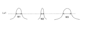
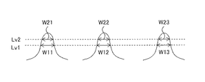
そこで、本実施の形態では、上述したように式(1)および式(2)を満たすように、LEDアレイ3と、レンズアレイ2と、感光体ドラム41との配置を設定している。そうすることで、図7Bに示したように、X軸方向に並ぶ複数のLED素子31の露光強度分布が互いに近似したものとなり、使用される露光強度(レベルLv1)において複数のLED素子31の光像径のばらつきを揃えることができる(W11≒W12≒W13)。仮に露光に使用される露光強度がレベルLv1からレベルLv2に変動した場合であっても、複数のLED素子31が互いに近似した露光強度分布を有するので、光像径のばらつきが生じにくい(W21≒W22≒W23)。すなわち、光学ヘッド1では、光像径の変動の少ない露光強度の範囲を使用して感光体ドラム41の露光がなされ、形成画像におけるすじや濃度むらなどが低減される。したがって、この光学ヘッド1を備えた画像形成装置100によれば、適切な露光を行うことができ、より良好な画像を形成することができる。
(実験例1)
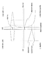
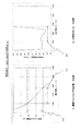
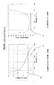
次に、上記実施の形態で説明した光学ヘッド1を作製し、LED素子31における、X軸方向の露光強度分布、および露光強度と光像径との関係について調査した。その結果を図8に示す。ここでは、ロッドレンズ21に、セルフォック(登録商標)レンズのSLA−12E(開口半角12°)を用い、LEDアレイ3の解像度を1200dpi(A4サイズ)とし、LED素子31の発光波長の中心値は740mm以上780mm以下に収まるようにした。ロッドレンズ21は、いずれも0.14mm〜0.16mmの半径を有し、屈折率分布の特性もほぼ同じものを用いた。さらに、レンズアレイ2の高さZ1は4.36mmとし、レンズアレイ2の焦点距離L0は2.38mmとした。また、距離ΔL1,ΔL2を共に+250μmとした。すなわち、距離L1,L2を焦点距離L0(=2.38mm)よりも250μm長くした。
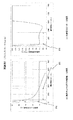
距離ΔL1,ΔL2を共に+200μmとした。この点を除き、他は実験例1と同様にして、LED素子31における、X軸方向の露光強度分布、および露光強度と光像径との関係について調査した。その結果を図9に示す。図9の(b)に示したように、本実験例では、露光強度範囲R1において光像径が大きく変動する結果となった。また、本実験例の光学ヘッド1を備えた画像形成装置100により画像形成(印刷)を行ったところ、印刷画像にすじおよび濃度むらが認められた。
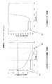
距離ΔL1,ΔL2を共に+150μmとした。この点を除き、他は実験例1と同様にして、LED素子31における、X軸方向の露光強度分布、および露光強度と光像径との関係について調査した。その結果を図10に示す。図10の(b)に示したように、本実験例では、露光強度範囲R1において光像径が大きく変動する結果となった。また、本実験例の光学ヘッド1を備えた画像形成装置100により画像形成(印刷)を行ったところ、印刷画像にすじおよび濃度むらが認められた。
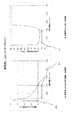
距離ΔL1,ΔL2を共に+50μmとした。この点を除き、他は実験例1と同様にして、LED素子31における、X軸方向の露光強度分布、および露光強度と光像径との関係について調査した。その結果を図11に示す。図11の(b)に示したように、本実験例では、露光強度範囲R1において光像径が大きく変動する結果となった。すなわち、本実験例では、露光強度範囲R1において光像径が突出して大きくなる箇所はなかったものの、露光強度範囲R1の上下限近傍において他の部分よりも光像径が大きくなった。また、本実験例の光学ヘッド1を備えた画像形成装置100により画像形成(印刷)を行ったところ、印刷画像にすじおよび濃度むらが認められた。
距離ΔL1,ΔL2を共に0μmとした。この点を除き、他は実験例1と同様にして、LED素子31における、X軸方向の露光強度分布、および露光強度と光像径との関係について調査した。その結果を図12に示す。図12の(b)に示したように、本実験例では、露光強度範囲R1において光像径が大きく変動する(突出する部分を含む)結果となった。また、本実験例の光学ヘッド1を備えた画像形成装置100により画像形成(印刷)を行ったところ、印刷画像にすじおよび濃度むらが認められた。
距離ΔL1,ΔL2を共に−150μmとした。この点を除き、他は実験例1と同様にして、LED素子31における、X軸方向の露光強度分布、および露光強度と光像径との関係について調査した。その結果を図13に示す。図13の(b)に示したように、本実験例では、露光強度範囲R1において光像径が大きく変動する(突出する部分を含む)結果となった。また、本実験例の光学ヘッド1を備えた画像形成装置100により画像形成(印刷)を行ったところ、印刷画像にすじおよび濃度むらが認められた。
距離ΔL1,ΔL2を共に−175μmとした。この点を除き、他は実験例1と同様にして、LED素子31における、X軸方向の露光強度分布、および露光強度と光像径との関係について調査した。その結果を図14に示す。図14の(b)に示したように、本実験例では、露光強度範囲R1において光像径が大きく変動する(突出する)部分はなく、良好な結果となった。また、本実験例の光学ヘッド1を備えた画像形成装置100により画像形成(印刷)を行ったところ、印刷画像にすじおよび濃度むらなどは認められなかった。
距離ΔL1,ΔL2を共に−200μmとした。この点を除き、他は実験例1と同様にして、LED素子31における、X軸方向の露光強度分布、および露光強度と光像径との関係について調査した。その結果を図15に示す。図15の(b)に示したように、本実験例においても、露光強度範囲R1において光像径が大きく変動する(突出する)部分はなく、良好な結果となった。また、本実験例の光学ヘッド1を備えた画像形成装置100により画像形成(印刷)を行ったところ、印刷画像にすじおよび濃度むらなどは認められなかった。
距離ΔL1,ΔL2を共に−250μmとした。この点を除き、他は実験例1と同様にして、LED素子31における、X軸方向の露光強度分布、および露光強度と光像径との関係について調査した。その結果を図16に示す。図16の(b)に示したように、本実験例においても、露光強度範囲R1において光像径が大きく変動する(突出する)部分はなく、良好な結果となった。また、本実験例の光学ヘッド1を備えた画像形成装置100により画像形成(印刷)を行ったところ、印刷画像にすじおよび濃度むらなどは認められなかった。
距離ΔL1,ΔL2を共に−300μmとした。この点を除き、他は実験例1と同様にして、LED素子31における、X軸方向の露光強度分布、および露光強度と光像径との関係について調査した。その結果を図17に示す。図17の(b)に示したように、本実験例では、露光強度範囲R1において光像径が突出して大きくなる箇所はなかったものの、露光強度範囲R1の上下限近傍において他の部分よりも光像径が大きくなった。また、本実験例の光学ヘッド1を備えた画像形成装置100により画像形成(印刷)を行ったところ、印刷画像にすじおよび濃度むらが認められた。
以上、実施の形態および変形例を挙げて本発明を説明したが、本発明はこれらの実施の形態等に限定されず、種々の変形が可能である。例えば、上記実施の形態では、レンズアレイ2が2列に並ぶロッドレンズ21を有するようにしたが、ロッドレンズの配置位置や数についてはこれに限定されるものではない。
Claims (6)
- 像担持体を露光する露光装置であって、
第1の方向に並んで光を各々発する複数の発光素子を含む発光素子アレイと、
前記第1の方向と直交する第2の方向において前記発光素子アレイと対向して配置され、前記複数の発光素子から各々発せられた複数の前記光を各々結像するレンズアレイと
を有し、
下記の式(1)および式(2)を満たす
露光装置。
175μm≦L0−L1≦250μm ……(1)
175μm≦L0−L2≦250μm ……(2)
但し、
L0:レンズアレイの焦点距離(レンズアレイにより結像された光の第1の方向の光量分布から算出したコントラストが最大となる距離)
L1:レンズアレイと発光素子アレイとの距離
L2:レンズアレイと像担持体との距離 - 前記レンズアレイは、開口半角が実質的に10°以上15°以下であると共に径方向において屈折率分布を有するロッドレンズを複数含む
請求項1記載の露光装置。 - 前記レンズアレイは、開口半角が実質的に12°であると共に径方向において屈折率分布を有するロッドレンズを複数含む
請求項1記載の露光装置。 - 前記ロッドレンズは、0.14mm以上0.16mm以下の半径と、4.2mm以上4.4mm以下の高さと、2.2mm以上2.5mm以下の焦点距離とを有するものである
請求項2または請求項3に記載の露光装置。 - 請求項1から請求項4のいずれか1項に記載の露光装置を備えた画像形成ユニット。
- 請求項1から請求項4のいずれか1項に記載の露光装置を備えた画像形成装置。
Priority Applications (4)
| Application Number | Priority Date | Filing Date | Title |
|---|---|---|---|
| JP2016009216A JP2017128045A (ja) | 2016-01-20 | 2016-01-20 | 露光装置、画像形成ユニットおよび画像形成装置 |
| EP16205340.9A EP3196703B1 (en) | 2016-01-20 | 2016-12-20 | Exposure unit, image forming unit, and image forming apparatus |
| US15/384,827 US20170205730A1 (en) | 2016-01-20 | 2016-12-20 | Exposure unit, image forming unit, and image forming apparatus |
| CN201611182452.1A CN106990687A (zh) | 2016-01-20 | 2016-12-20 | 曝光装置、图像形成单元和图像形成装置 |
Applications Claiming Priority (1)
| Application Number | Priority Date | Filing Date | Title |
|---|---|---|---|
| JP2016009216A JP2017128045A (ja) | 2016-01-20 | 2016-01-20 | 露光装置、画像形成ユニットおよび画像形成装置 |
Publications (1)
| Publication Number | Publication Date |
|---|---|
| JP2017128045A true JP2017128045A (ja) | 2017-07-27 |
Family
ID=57570814
Family Applications (1)
| Application Number | Title | Priority Date | Filing Date |
|---|---|---|---|
| JP2016009216A Pending JP2017128045A (ja) | 2016-01-20 | 2016-01-20 | 露光装置、画像形成ユニットおよび画像形成装置 |
Country Status (4)
| Country | Link |
|---|---|
| US (1) | US20170205730A1 (ja) |
| EP (1) | EP3196703B1 (ja) |
| JP (1) | JP2017128045A (ja) |
| CN (1) | CN106990687A (ja) |
Families Citing this family (1)
| Publication number | Priority date | Publication date | Assignee | Title |
|---|---|---|---|---|
| US10496003B2 (en) * | 2017-09-04 | 2019-12-03 | Fuji Xerox Co., Ltd. | Exposure device |
Citations (7)
| Publication number | Priority date | Publication date | Assignee | Title |
|---|---|---|---|---|
| JPH0422248U (ja) * | 1990-06-18 | 1992-02-25 | ||
| US5543830A (en) * | 1990-10-12 | 1996-08-06 | Minnesota Mining And Manufacturing Company | Apparatus with light emitting element, microlens and gradient index lens characteristics for imaging continuous tone images |
| JPH11188910A (ja) * | 1997-12-26 | 1999-07-13 | Ricoh Co Ltd | 画像形成装置 |
| JPH11231212A (ja) * | 1998-02-13 | 1999-08-27 | Nippon Sheet Glass Co Ltd | 結像光学装置 |
| JP2000221442A (ja) * | 1999-01-28 | 2000-08-11 | Nippon Sheet Glass Co Ltd | 結像光学装置 |
| JP2002144626A (ja) * | 2000-11-15 | 2002-05-22 | Ricoh Co Ltd | 光プリントヘッド及び画像形成装置 |
| JP2010221510A (ja) * | 2009-03-23 | 2010-10-07 | Fuji Xerox Co Ltd | 露光装置及び画像形成装置 |
Family Cites Families (9)
| Publication number | Priority date | Publication date | Assignee | Title |
|---|---|---|---|---|
| US3973954A (en) * | 1973-12-28 | 1976-08-10 | Xerox Corporation | Imaging method including exposure of photoconductive imaging member through lenticular lens element |
| DK300689A (da) * | 1988-06-21 | 1989-12-22 | Rohm Co Ltd | Apparat til optisk skrivning af informationer |
| US6031668A (en) * | 1997-12-24 | 2000-02-29 | Nippon Sheet Glass Co., Ltd. | Optical imaging system |
| TW504588B (en) * | 2000-09-22 | 2002-10-01 | Nippon Sheet Glass Co Ltd | Array of rod lenses used in scanner |
| JP4416581B2 (ja) * | 2004-06-30 | 2010-02-17 | 株式会社沖データ | 露光装置、ledプリントヘッド及びこれを備えた画像形成装置 |
| JP2006056768A (ja) * | 2004-07-23 | 2006-03-02 | Nippon Sheet Glass Co Ltd | 屈折率分布型ロッドレンズ用クラッドガラス組成物、およびそれを用いた屈折率分布型ロッドレンズ母ガラスロッド、ならびに屈折率分布型ロッドレンズ、およびその製造方法 |
| JP5196145B2 (ja) * | 2007-10-03 | 2013-05-15 | セイコーエプソン株式会社 | ラインヘッド及びそれを用いた画像形成装置 |
| JP2013014044A (ja) * | 2011-07-01 | 2013-01-24 | Canon Inc | 画像形成装置 |
| US9081322B2 (en) * | 2013-12-16 | 2015-07-14 | Xerox Corporation | LED printhead with relay lens to increase depth of focus |
-
2016
- 2016-01-20 JP JP2016009216A patent/JP2017128045A/ja active Pending
- 2016-12-20 US US15/384,827 patent/US20170205730A1/en not_active Abandoned
- 2016-12-20 CN CN201611182452.1A patent/CN106990687A/zh active Pending
- 2016-12-20 EP EP16205340.9A patent/EP3196703B1/en active Active
Patent Citations (7)
| Publication number | Priority date | Publication date | Assignee | Title |
|---|---|---|---|---|
| JPH0422248U (ja) * | 1990-06-18 | 1992-02-25 | ||
| US5543830A (en) * | 1990-10-12 | 1996-08-06 | Minnesota Mining And Manufacturing Company | Apparatus with light emitting element, microlens and gradient index lens characteristics for imaging continuous tone images |
| JPH11188910A (ja) * | 1997-12-26 | 1999-07-13 | Ricoh Co Ltd | 画像形成装置 |
| JPH11231212A (ja) * | 1998-02-13 | 1999-08-27 | Nippon Sheet Glass Co Ltd | 結像光学装置 |
| JP2000221442A (ja) * | 1999-01-28 | 2000-08-11 | Nippon Sheet Glass Co Ltd | 結像光学装置 |
| JP2002144626A (ja) * | 2000-11-15 | 2002-05-22 | Ricoh Co Ltd | 光プリントヘッド及び画像形成装置 |
| JP2010221510A (ja) * | 2009-03-23 | 2010-10-07 | Fuji Xerox Co Ltd | 露光装置及び画像形成装置 |
Also Published As
| Publication number | Publication date |
|---|---|
| CN106990687A (zh) | 2017-07-28 |
| US20170205730A1 (en) | 2017-07-20 |
| EP3196703B1 (en) | 2019-02-27 |
| EP3196703A1 (en) | 2017-07-26 |
Similar Documents
| Publication | Publication Date | Title |
|---|---|---|
| US8494426B2 (en) | Laser fixing device and image forming apparatus including the same | |
| US10591842B2 (en) | Lens array, lens unit, exposure device, LED head, and image forming apparatus | |
| JP6334372B2 (ja) | 印刷媒体供給装置および画像形成装置 | |
| JP4374970B2 (ja) | 画像形成装置 | |
| JP6070679B2 (ja) | 画像形成装置及び濃度補正方法 | |
| JP4733576B2 (ja) | 画像形成装置 | |
| CN100444039C (zh) | 显影盒及具有其的电子照相成像设备 | |
| JP2014021432A (ja) | レンズホルダ、レンズユニット、ledヘッド、露光装置、画像形成装置及び読取装置 | |
| EP3196703B1 (en) | Exposure unit, image forming unit, and image forming apparatus | |
| JP4656877B2 (ja) | 除電装置 | |
| JP2008268273A (ja) | 光除電装置、像保持体ユニット、画像形成ユニットおよび画像形成装置 | |
| US9448530B1 (en) | Developer storage body, image forming unit and image forming apparatus | |
| US20180321611A1 (en) | Image forming apparatus and photosensitive member unit | |
| CN106997162B (zh) | 曝光装置、图像形成单元和图像形成装置 | |
| KR101079578B1 (ko) | 물성이 상이한 복수의 현상제를 갖는 현상카트리지 및 이를포함하는 화상형성장치 | |
| JP5929042B2 (ja) | 画像形成装置 | |
| JP2009109811A (ja) | 画像形成装置及び画像形成方法 | |
| US20060147230A1 (en) | Image forming apparatus | |
| JP2005114976A (ja) | 画像形成装置 | |
| JP2026042294A (ja) | 露光装置および画像形成装置 | |
| KR100423459B1 (ko) | 칼라 화상형성장치 | |
| JP5803343B2 (ja) | 画像形成装置 | |
| JP2016188934A (ja) | 画像形成装置 | |
| US9400452B2 (en) | Image forming unit having image carrier, developer carrier that supplies developer to image carrier and developer supply member that supplies developer to developer carrier, and image forming apparatus having image carrier, developer carrier that supplies developer to image carrier and developer supply member that supplies developer to developer carrier | |
| JP2010091909A (ja) | Led光学素子、画像形成装置及び画像形成方法 |
Legal Events
| Date | Code | Title | Description |
|---|---|---|---|
| A621 | Written request for application examination |
Free format text: JAPANESE INTERMEDIATE CODE: A621 Effective date: 20180615 |
|
| A977 | Report on retrieval |
Free format text: JAPANESE INTERMEDIATE CODE: A971007 Effective date: 20190208 |
|
| A131 | Notification of reasons for refusal |
Free format text: JAPANESE INTERMEDIATE CODE: A131 Effective date: 20190219 |
|
| A521 | Request for written amendment filed |
Free format text: JAPANESE INTERMEDIATE CODE: A523 Effective date: 20190419 |
|
| A02 | Decision of refusal |
Free format text: JAPANESE INTERMEDIATE CODE: A02 Effective date: 20190702 |