JP2017129629A - パターン検査装置 - Google Patents
パターン検査装置 Download PDFInfo
- Publication number
- JP2017129629A JP2017129629A JP2016007206A JP2016007206A JP2017129629A JP 2017129629 A JP2017129629 A JP 2017129629A JP 2016007206 A JP2016007206 A JP 2016007206A JP 2016007206 A JP2016007206 A JP 2016007206A JP 2017129629 A JP2017129629 A JP 2017129629A
- Authority
- JP
- Japan
- Prior art keywords
- pattern
- image
- light
- inspection
- line
- Prior art date
- Legal status (The legal status is an assumption and is not a legal conclusion. Google has not performed a legal analysis and makes no representation as to the accuracy of the status listed.)
- Granted
Links
Images





Classifications
-
- G—PHYSICS
- G03—PHOTOGRAPHY; CINEMATOGRAPHY; ANALOGOUS TECHNIQUES USING WAVES OTHER THAN OPTICAL WAVES; ELECTROGRAPHY; HOLOGRAPHY
- G03F—PHOTOMECHANICAL PRODUCTION OF TEXTURED OR PATTERNED SURFACES, e.g. FOR PRINTING, FOR PROCESSING OF SEMICONDUCTOR DEVICES; MATERIALS THEREFOR; ORIGINALS THEREFOR; APPARATUS SPECIALLY ADAPTED THEREFOR
- G03F1/00—Originals for photomechanical production of textured or patterned surfaces, e.g., masks, photo-masks, reticles; Mask blanks or pellicles therefor; Containers specially adapted therefor; Preparation thereof
- G03F1/68—Preparation processes not covered by groups G03F1/20 - G03F1/50
- G03F1/82—Auxiliary processes, e.g. cleaning or inspecting
- G03F1/84—Inspecting
-
- G—PHYSICS
- G03—PHOTOGRAPHY; CINEMATOGRAPHY; ANALOGOUS TECHNIQUES USING WAVES OTHER THAN OPTICAL WAVES; ELECTROGRAPHY; HOLOGRAPHY
- G03F—PHOTOMECHANICAL PRODUCTION OF TEXTURED OR PATTERNED SURFACES, e.g. FOR PRINTING, FOR PROCESSING OF SEMICONDUCTOR DEVICES; MATERIALS THEREFOR; ORIGINALS THEREFOR; APPARATUS SPECIALLY ADAPTED THEREFOR
- G03F7/00—Photomechanical, e.g. photolithographic, production of textured or patterned surfaces, e.g. printing surfaces; Materials therefor, e.g. comprising photoresists; Apparatus specially adapted therefor
- G03F7/70—Microphotolithographic exposure; Apparatus therefor
- G03F7/70483—Information management; Active and passive control; Testing; Wafer monitoring, e.g. pattern monitoring
- G03F7/70605—Workpiece metrology
- G03F7/70616—Monitoring the printed patterns
-
- G—PHYSICS
- G03—PHOTOGRAPHY; CINEMATOGRAPHY; ANALOGOUS TECHNIQUES USING WAVES OTHER THAN OPTICAL WAVES; ELECTROGRAPHY; HOLOGRAPHY
- G03F—PHOTOMECHANICAL PRODUCTION OF TEXTURED OR PATTERNED SURFACES, e.g. FOR PRINTING, FOR PROCESSING OF SEMICONDUCTOR DEVICES; MATERIALS THEREFOR; ORIGINALS THEREFOR; APPARATUS SPECIALLY ADAPTED THEREFOR
- G03F7/00—Photomechanical, e.g. photolithographic, production of textured or patterned surfaces, e.g. printing surfaces; Materials therefor, e.g. comprising photoresists; Apparatus specially adapted therefor
- G03F7/70—Microphotolithographic exposure; Apparatus therefor
- G03F7/70058—Mask illumination systems
- G03F7/70141—Illumination system adjustment, e.g. adjustments during exposure or alignment during assembly of illumination system
-
- G—PHYSICS
- G03—PHOTOGRAPHY; CINEMATOGRAPHY; ANALOGOUS TECHNIQUES USING WAVES OTHER THAN OPTICAL WAVES; ELECTROGRAPHY; HOLOGRAPHY
- G03F—PHOTOMECHANICAL PRODUCTION OF TEXTURED OR PATTERNED SURFACES, e.g. FOR PRINTING, FOR PROCESSING OF SEMICONDUCTOR DEVICES; MATERIALS THEREFOR; ORIGINALS THEREFOR; APPARATUS SPECIALLY ADAPTED THEREFOR
- G03F7/00—Photomechanical, e.g. photolithographic, production of textured or patterned surfaces, e.g. printing surfaces; Materials therefor, e.g. comprising photoresists; Apparatus specially adapted therefor
- G03F7/70—Microphotolithographic exposure; Apparatus therefor
- G03F7/70058—Mask illumination systems
- G03F7/702—Reflective illumination, i.e. reflective optical elements other than folding mirrors, e.g. extreme ultraviolet [EUV] illumination systems
-
- G—PHYSICS
- G03—PHOTOGRAPHY; CINEMATOGRAPHY; ANALOGOUS TECHNIQUES USING WAVES OTHER THAN OPTICAL WAVES; ELECTROGRAPHY; HOLOGRAPHY
- G03F—PHOTOMECHANICAL PRODUCTION OF TEXTURED OR PATTERNED SURFACES, e.g. FOR PRINTING, FOR PROCESSING OF SEMICONDUCTOR DEVICES; MATERIALS THEREFOR; ORIGINALS THEREFOR; APPARATUS SPECIALLY ADAPTED THEREFOR
- G03F7/00—Photomechanical, e.g. photolithographic, production of textured or patterned surfaces, e.g. printing surfaces; Materials therefor, e.g. comprising photoresists; Apparatus specially adapted therefor
- G03F7/70—Microphotolithographic exposure; Apparatus therefor
- G03F7/70216—Mask projection systems
- G03F7/70275—Multiple projection paths, e.g. array of projection systems, microlens projection systems or tandem projection systems
-
- G—PHYSICS
- G03—PHOTOGRAPHY; CINEMATOGRAPHY; ANALOGOUS TECHNIQUES USING WAVES OTHER THAN OPTICAL WAVES; ELECTROGRAPHY; HOLOGRAPHY
- G03F—PHOTOMECHANICAL PRODUCTION OF TEXTURED OR PATTERNED SURFACES, e.g. FOR PRINTING, FOR PROCESSING OF SEMICONDUCTOR DEVICES; MATERIALS THEREFOR; ORIGINALS THEREFOR; APPARATUS SPECIALLY ADAPTED THEREFOR
- G03F7/00—Photomechanical, e.g. photolithographic, production of textured or patterned surfaces, e.g. printing surfaces; Materials therefor, e.g. comprising photoresists; Apparatus specially adapted therefor
- G03F7/70—Microphotolithographic exposure; Apparatus therefor
- G03F7/70483—Information management; Active and passive control; Testing; Wafer monitoring, e.g. pattern monitoring
- G03F7/70605—Workpiece metrology
- G03F7/706835—Metrology information management or control
-
- G—PHYSICS
- G03—PHOTOGRAPHY; CINEMATOGRAPHY; ANALOGOUS TECHNIQUES USING WAVES OTHER THAN OPTICAL WAVES; ELECTROGRAPHY; HOLOGRAPHY
- G03F—PHOTOMECHANICAL PRODUCTION OF TEXTURED OR PATTERNED SURFACES, e.g. FOR PRINTING, FOR PROCESSING OF SEMICONDUCTOR DEVICES; MATERIALS THEREFOR; ORIGINALS THEREFOR; APPARATUS SPECIALLY ADAPTED THEREFOR
- G03F7/00—Photomechanical, e.g. photolithographic, production of textured or patterned surfaces, e.g. printing surfaces; Materials therefor, e.g. comprising photoresists; Apparatus specially adapted therefor
- G03F7/70—Microphotolithographic exposure; Apparatus therefor
- G03F7/70483—Information management; Active and passive control; Testing; Wafer monitoring, e.g. pattern monitoring
- G03F7/70605—Workpiece metrology
- G03F7/706843—Metrology apparatus
-
- G—PHYSICS
- G03—PHOTOGRAPHY; CINEMATOGRAPHY; ANALOGOUS TECHNIQUES USING WAVES OTHER THAN OPTICAL WAVES; ELECTROGRAPHY; HOLOGRAPHY
- G03F—PHOTOMECHANICAL PRODUCTION OF TEXTURED OR PATTERNED SURFACES, e.g. FOR PRINTING, FOR PROCESSING OF SEMICONDUCTOR DEVICES; MATERIALS THEREFOR; ORIGINALS THEREFOR; APPARATUS SPECIALLY ADAPTED THEREFOR
- G03F7/00—Photomechanical, e.g. photolithographic, production of textured or patterned surfaces, e.g. printing surfaces; Materials therefor, e.g. comprising photoresists; Apparatus specially adapted therefor
- G03F7/70—Microphotolithographic exposure; Apparatus therefor
- G03F7/708—Construction of apparatus, e.g. environment aspects, hygiene aspects or materials
- G03F7/70808—Construction details, e.g. housing, load-lock, seals or windows for passing light in or out of apparatus
- G03F7/70833—Mounting of optical systems, e.g. mounting of illumination system, projection system or stage systems on base-plate or ground
-
- G—PHYSICS
- G03—PHOTOGRAPHY; CINEMATOGRAPHY; ANALOGOUS TECHNIQUES USING WAVES OTHER THAN OPTICAL WAVES; ELECTROGRAPHY; HOLOGRAPHY
- G03F—PHOTOMECHANICAL PRODUCTION OF TEXTURED OR PATTERNED SURFACES, e.g. FOR PRINTING, FOR PROCESSING OF SEMICONDUCTOR DEVICES; MATERIALS THEREFOR; ORIGINALS THEREFOR; APPARATUS SPECIALLY ADAPTED THEREFOR
- G03F7/00—Photomechanical, e.g. photolithographic, production of textured or patterned surfaces, e.g. printing surfaces; Materials therefor, e.g. comprising photoresists; Apparatus specially adapted therefor
- G03F7/70—Microphotolithographic exposure; Apparatus therefor
- G03F7/708—Construction of apparatus, e.g. environment aspects, hygiene aspects or materials
- G03F7/7085—Detection arrangement, e.g. detectors of apparatus alignment possibly mounted on wafers, exposure dose, photo-cleaning flux, stray light, thermal load
-
- G—PHYSICS
- G06—COMPUTING OR CALCULATING; COUNTING
- G06T—IMAGE DATA PROCESSING OR GENERATION, IN GENERAL
- G06T7/00—Image analysis
- G06T7/0002—Inspection of images, e.g. flaw detection
- G06T7/0004—Industrial image inspection
- G06T7/001—Industrial image inspection using an image reference approach
-
- G—PHYSICS
- G06—COMPUTING OR CALCULATING; COUNTING
- G06T—IMAGE DATA PROCESSING OR GENERATION, IN GENERAL
- G06T7/00—Image analysis
- G06T7/70—Determining position or orientation of objects or cameras
- G06T7/73—Determining position or orientation of objects or cameras using feature-based methods
- G06T7/74—Determining position or orientation of objects or cameras using feature-based methods involving reference images or patches
-
- G—PHYSICS
- G06—COMPUTING OR CALCULATING; COUNTING
- G06V—IMAGE OR VIDEO RECOGNITION OR UNDERSTANDING
- G06V10/00—Arrangements for image or video recognition or understanding
- G06V10/10—Image acquisition
- G06V10/12—Details of acquisition arrangements; Constructional details thereof
- G06V10/14—Optical characteristics of the device performing the acquisition or on the illumination arrangements
- G06V10/147—Details of sensors, e.g. sensor lenses
-
- G—PHYSICS
- G06—COMPUTING OR CALCULATING; COUNTING
- G06V—IMAGE OR VIDEO RECOGNITION OR UNDERSTANDING
- G06V10/00—Arrangements for image or video recognition or understanding
- G06V10/70—Arrangements for image or video recognition or understanding using pattern recognition or machine learning
- G06V10/74—Image or video pattern matching; Proximity measures in feature spaces
- G06V10/75—Organisation of the matching processes, e.g. simultaneous or sequential comparisons of image or video features; Coarse-fine approaches, e.g. multi-scale approaches; using context analysis; Selection of dictionaries
- G06V10/751—Comparing pixel values or logical combinations thereof, or feature values having positional relevance, e.g. template matching
- G06V10/7515—Shifting the patterns to accommodate for positional errors
-
- H—ELECTRICITY
- H04—ELECTRIC COMMUNICATION TECHNIQUE
- H04N—PICTORIAL COMMUNICATION, e.g. TELEVISION
- H04N23/00—Cameras or camera modules comprising electronic image sensors; Control thereof
- H04N23/45—Cameras or camera modules comprising electronic image sensors; Control thereof for generating image signals from two or more image sensors being of different type or operating in different modes, e.g. with a CMOS sensor for moving images in combination with a charge-coupled device [CCD] for still images
-
- H—ELECTRICITY
- H04—ELECTRIC COMMUNICATION TECHNIQUE
- H04N—PICTORIAL COMMUNICATION, e.g. TELEVISION
- H04N23/00—Cameras or camera modules comprising electronic image sensors; Control thereof
- H04N23/56—Cameras or camera modules comprising electronic image sensors; Control thereof provided with illuminating means
-
- H—ELECTRICITY
- H04—ELECTRIC COMMUNICATION TECHNIQUE
- H04N—PICTORIAL COMMUNICATION, e.g. TELEVISION
- H04N23/00—Cameras or camera modules comprising electronic image sensors; Control thereof
- H04N23/70—Circuitry for compensating brightness variation in the scene
- H04N23/71—Circuitry for evaluating the brightness variation
-
- G—PHYSICS
- G01—MEASURING; TESTING
- G01N—INVESTIGATING OR ANALYSING MATERIALS BY DETERMINING THEIR CHEMICAL OR PHYSICAL PROPERTIES
- G01N21/00—Investigating or analysing materials by the use of optical means, i.e. using sub-millimetre waves, infrared, visible or ultraviolet light
- G01N21/84—Systems specially adapted for particular applications
- G01N21/88—Investigating the presence of flaws or contamination
- G01N21/95—Investigating the presence of flaws or contamination characterised by the material or shape of the object to be examined
- G01N21/956—Inspecting patterns on the surface of objects
- G01N2021/95676—Masks, reticles, shadow masks
-
- G—PHYSICS
- G01—MEASURING; TESTING
- G01N—INVESTIGATING OR ANALYSING MATERIALS BY DETERMINING THEIR CHEMICAL OR PHYSICAL PROPERTIES
- G01N21/00—Investigating or analysing materials by the use of optical means, i.e. using sub-millimetre waves, infrared, visible or ultraviolet light
- G01N21/84—Systems specially adapted for particular applications
- G01N21/88—Investigating the presence of flaws or contamination
- G01N21/95—Investigating the presence of flaws or contamination characterised by the material or shape of the object to be examined
- G01N21/956—Inspecting patterns on the surface of objects
- G01N21/95607—Inspecting patterns on the surface of objects using a comparative method
-
- G—PHYSICS
- G06—COMPUTING OR CALCULATING; COUNTING
- G06T—IMAGE DATA PROCESSING OR GENERATION, IN GENERAL
- G06T2207/00—Indexing scheme for image analysis or image enhancement
- G06T2207/30—Subject of image; Context of image processing
- G06T2207/30108—Industrial image inspection
- G06T2207/30148—Semiconductor; IC; Wafer
-
- H—ELECTRICITY
- H04—ELECTRIC COMMUNICATION TECHNIQUE
- H04N—PICTORIAL COMMUNICATION, e.g. TELEVISION
- H04N25/00—Circuitry of solid-state image sensors [SSIS]; Control thereof
- H04N25/70—SSIS architectures; Circuits associated therewith
- H04N25/71—Charge-coupled device [CCD] sensors; Charge-transfer registers specially adapted for CCD sensors
-
- H—ELECTRICITY
- H04—ELECTRIC COMMUNICATION TECHNIQUE
- H04N—PICTORIAL COMMUNICATION, e.g. TELEVISION
- H04N25/00—Circuitry of solid-state image sensors [SSIS]; Control thereof
- H04N25/70—SSIS architectures; Circuits associated therewith
- H04N25/76—Addressed sensors, e.g. MOS or CMOS sensors
- H04N25/768—Addressed sensors, e.g. MOS or CMOS sensors for time delay and integration [TDI]
Landscapes
- Engineering & Computer Science (AREA)
- Physics & Mathematics (AREA)
- General Physics & Mathematics (AREA)
- Theoretical Computer Science (AREA)
- Multimedia (AREA)
- Computer Vision & Pattern Recognition (AREA)
- Health & Medical Sciences (AREA)
- General Health & Medical Sciences (AREA)
- Signal Processing (AREA)
- Environmental & Geological Engineering (AREA)
- Epidemiology (AREA)
- Quality & Reliability (AREA)
- Public Health (AREA)
- Databases & Information Systems (AREA)
- Medical Informatics (AREA)
- Vascular Medicine (AREA)
- Evolutionary Computation (AREA)
- Computing Systems (AREA)
- Artificial Intelligence (AREA)
- Software Systems (AREA)
- Human Computer Interaction (AREA)
- Investigating Materials By The Use Of Optical Means Adapted For Particular Applications (AREA)
- Length Measuring Devices By Optical Means (AREA)
- Testing Or Measuring Of Semiconductors Or The Like (AREA)
- Preparing Plates And Mask In Photomechanical Process (AREA)
- Life Sciences & Earth Sciences (AREA)
- Immunology (AREA)
- Pathology (AREA)
- Biochemistry (AREA)
- Analytical Chemistry (AREA)
- Chemical & Material Sciences (AREA)
Abstract
Description
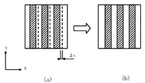
パターンが形成された基板に反射照明光を照明する反射照明光学系と、
反射照明光学系の光路中に配置され、反射照明光の一部の照射を受ける、ラインアンドスペースパターンによる第1の基準パターンが形成された第1の絞りと、
第1の基準パターンを通過した基準パターン像の一部を反射する半透過反射板と、
基板のパターン像を結像させる結像光学系と、
結像光学系の光路中に配置され、半透過反射板によって反射された基準パターン像の上述した一部が投影される、ラインアンドスペースパターンによる第2の基準パターンが形成された第2の絞りと、
第2の基準パターンを通過した基準パターン像の上述した一部を受光するタイム・ディレイ・インテグレーションセンサ(TDIセンサ)と、
を備えたことを特徴とする。
複数の受光素子の一部により、変位量演算用の光が受光され、複数の受光素子の残部により、基板のパターン像が撮像され、
演算された変位量を用いて、基板のパターン像と参照画像との相対位置を補正する補正部と、
補正された位置関係で基板のパターン像と参照画像とを比較する比較部と、
をさらに備えると好適である。
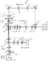
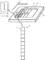
図1は、実施の形態1におけるパターン検査装置の構成を示す構成図である。図1において、マスク基板101(検査対象基板の一例)に形成されたパターンの欠陥を検査する検査装置100は、光学画像取得部150、及び制御系回路160(制御部)を備えている。
(1) Δx=k・(Q2−Q1)/(Q1+Q2)
(2) Δx=k・(Q1−Q2)/(Q1+Q2)
20 検査ストライプ
30 フレーム領域
61 ビームスプリッタ
62 レンズ
63 ミラー
64,65 レンズ
67 ミラー
68 コンデンサレンズ
69 レンズ
70,72 レンズ
73 ミラー
74,75,76 レンズ
80,81,82 レンズ
100 検査装置
101 マスク基板
102 XYθテーブル
103 光源
104 対物レンズ
105,205 TDIセンサ
106,206 センサ回路
107 位置回路
108 比較回路
109 磁気ディスク装置
110 制御計算機
111 展開回路
112 参照回路
113 オートローダ制御回路
114 テーブル制御回路
115 磁気テープ装置
116 FD
117 CRT
118 パターンモニタ
119 プリンタ
120 バス
122 レーザ測長システム
123,223 ストライプパターンメモリ
150 光学画像取得部
160 制御系回路
170 透過照明光学系
172 反射照明光学系
174 ビームスプリッタ
176,178 結像光学系
180 半透過反射板
182,184 結像光学系
Claims (5)
- パターンが形成された基板に反射照明光を照明する反射照明光学系と、
前記反射照明光学系の光路中に配置され、前記反射照明光の一部の照射を受ける、ラインアンドスペースパターンによる第1の基準パターンが形成された第1の絞りと、
前記第1の基準パターンを通過した基準パターン像の一部を反射する半透過反射板と、
前記基板のパターン像を結像させる結像光学系と、
前記結像光学系の光路中に配置され、前記半透過反射板によって反射された前記基準パターン像の前記一部が投影される、ラインアンドスペースパターンによる第2の基準パターンが形成された第2の絞りと、
前記第2の基準パターンを通過した前記基準パターン像の前記一部を受光するタイム・ディレイ・インテグレーションセンサ(TDIセンサ)と、
を備えたことを特徴とするパターン検査装置。 - 前記TDIセンサによって受光される前記基準パターン像の前記一部の光量変化に係数を乗じることによって空気ゆらぎの変位量を演算する演算部をさらに備えたことを特徴とする請求項1記載のパターン検査装置。
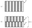
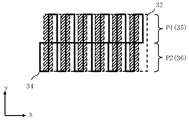
- 前記第1と第2の基準パターンの一方は、2段のラインアンドスペースパターンが、逆のパターン種が接続されるように配置され、他方は、1段のラインアンドスペースパターンが配置されることを特徴とする請求項1又は2記載のパターン検査装置。
- 前記2段のラインアンドスペースパターンの一方のラインアンドスペースパターンを通過した光量から他方のラインアンドスペースパターンを通過した光量を差し引いた差分を前記一方のラインアンドスペースパターンを通過した光量と前記他方のラインアンドスペースパターンを通過した光量と和で割った値に前記係数を乗じることによって、前記変位量を演算することを特徴とする請求項2記載のパターン検査装置。
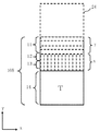
- 前記TDIセンサは、2次元状に配列された複数の受光素子を有し、
前記複数の受光素子の一部により、前記変位量演算用の光が受光され、前記複数の受光素子の残部により、前記基板のパターン像が撮像され、
演算された前記変位量を用いて、前記基板のパターン像と参照画像との相対位置を補正する補正部と、
補正された位置関係で前記基板のパターン像と前記参照画像とを比較する比較部と、
をさらに備えたことを特徴とする請求項2又は4記載のパターン検査装置。
Priority Applications (4)
| Application Number | Priority Date | Filing Date | Title |
|---|---|---|---|
| JP2016007206A JP6633918B2 (ja) | 2016-01-18 | 2016-01-18 | パターン検査装置 |
| US15/407,397 US10282635B2 (en) | 2016-01-18 | 2017-01-17 | Pattern inspection apparatus |
| DE102017200628.5A DE102017200628B4 (de) | 2016-01-18 | 2017-01-17 | Musterprüfvorrichtung |
| KR1020170008561A KR101882837B1 (ko) | 2016-01-18 | 2017-01-18 | 패턴 검사 장치 |
Applications Claiming Priority (1)
| Application Number | Priority Date | Filing Date | Title |
|---|---|---|---|
| JP2016007206A JP6633918B2 (ja) | 2016-01-18 | 2016-01-18 | パターン検査装置 |
Publications (2)
| Publication Number | Publication Date |
|---|---|
| JP2017129629A true JP2017129629A (ja) | 2017-07-27 |
| JP6633918B2 JP6633918B2 (ja) | 2020-01-22 |
Family
ID=59256212
Family Applications (1)
| Application Number | Title | Priority Date | Filing Date |
|---|---|---|---|
| JP2016007206A Active JP6633918B2 (ja) | 2016-01-18 | 2016-01-18 | パターン検査装置 |
Country Status (4)
| Country | Link |
|---|---|
| US (1) | US10282635B2 (ja) |
| JP (1) | JP6633918B2 (ja) |
| KR (1) | KR101882837B1 (ja) |
| DE (1) | DE102017200628B4 (ja) |
Families Citing this family (7)
| Publication number | Priority date | Publication date | Assignee | Title |
|---|---|---|---|---|
| DE102017203879B4 (de) * | 2017-03-09 | 2023-06-07 | Carl Zeiss Smt Gmbh | Verfahren zum Analysieren einer defekten Stelle einer photolithographischen Maske |
| JP7079569B2 (ja) * | 2017-04-21 | 2022-06-02 | 株式会社ニューフレアテクノロジー | 検査方法 |
| TWI628415B (zh) * | 2017-09-13 | 2018-07-01 | 國立清華大學 | 基於影像尺的定位量測系統 |
| KR20220036934A (ko) | 2019-06-28 | 2022-03-23 | 에도 왁스 | 소형 이미징 시스템을 사용한 고배율 고해상도 촬영을 위한 시스템 및 방법 |
| US11263741B2 (en) * | 2020-01-24 | 2022-03-01 | Applied Materials Israel Ltd. | System and methods of generating comparable regions of a lithographic mask |
| KR102836687B1 (ko) * | 2020-05-11 | 2025-07-22 | 삼성디스플레이 주식회사 | 마스크 검사 장치 및 이를 이용한 마스크 검사 방법 |
| JP7604354B2 (ja) * | 2021-10-29 | 2024-12-23 | 株式会社ニューフレアテクノロジー | 検査装置及び焦点位置調整方法 |
Citations (4)
| Publication number | Priority date | Publication date | Assignee | Title |
|---|---|---|---|---|
| JPH07106243A (ja) * | 1993-03-15 | 1995-04-21 | Nikon Corp | 水平位置検出装置 |
| JP2000082654A (ja) * | 1998-09-03 | 2000-03-21 | Canon Inc | 面位置検出装置及びそれを用いたデバイスの製造方法 |
| JP2002122553A (ja) * | 2000-10-18 | 2002-04-26 | Lasertec Corp | 撮像装置及びフォトマスクの欠陥検査装置 |
| JP2011257164A (ja) * | 2010-06-07 | 2011-12-22 | Toshiba Corp | パターン検査装置 |
Family Cites Families (15)
| Publication number | Priority date | Publication date | Assignee | Title |
|---|---|---|---|---|
| US5424552A (en) * | 1991-07-09 | 1995-06-13 | Nikon Corporation | Projection exposing apparatus |
| JP3291818B2 (ja) * | 1993-03-16 | 2002-06-17 | 株式会社ニコン | 投影露光装置、及び該装置を用いる半導体集積回路製造方法 |
| US6151122A (en) * | 1995-02-21 | 2000-11-21 | Nikon Corporation | Inspection method and apparatus for projection optical systems |
| JP2003068622A (ja) * | 2001-08-28 | 2003-03-07 | Canon Inc | 露光装置及びその制御方法並びにデバイスの製造方法 |
| JP2009300426A (ja) | 2008-05-16 | 2009-12-24 | Nuflare Technology Inc | レチクル欠陥検査装置およびレチクル欠陥検査方法 |
| JP2011169743A (ja) | 2010-02-18 | 2011-09-01 | Nuflare Technology Inc | 検査装置および検査方法 |
| NL2007615A (en) * | 2010-11-30 | 2012-05-31 | Asml Netherlands Bv | Method of operating a patterning device and lithographic apparatus. |
| JP5921990B2 (ja) * | 2012-08-23 | 2016-05-24 | 株式会社ニューフレアテクノロジー | 欠陥検出方法 |
| JP6025489B2 (ja) | 2012-10-11 | 2016-11-16 | 株式会社ニューフレアテクノロジー | 検査装置および検査装置システム |
| JP6043583B2 (ja) * | 2012-10-23 | 2016-12-14 | 株式会社ニューフレアテクノロジー | 焦点位置検出装置、検査装置、焦点位置検出方法および検査方法 |
| JP5944850B2 (ja) * | 2013-03-11 | 2016-07-05 | 株式会社日立ハイテクノロジーズ | 欠陥検査方法及びこれを用いた装置 |
| JP2016008941A (ja) * | 2014-06-26 | 2016-01-18 | 株式会社日立ハイテクノロジーズ | 欠陥観察方法及びその装置並びに欠陥検出装置 |
| JP2016007206A (ja) | 2014-06-26 | 2016-01-18 | キリン・トロピカーナ株式会社 | ココナッツ果汁入り飲料 |
| JP2017009379A (ja) * | 2015-06-19 | 2017-01-12 | 株式会社ニューフレアテクノロジー | 検査装置および検査方法 |
| WO2018046278A1 (en) * | 2016-09-06 | 2018-03-15 | Asml Holding N.V. | Method and device for focusing in an inspection system |
-
2016
- 2016-01-18 JP JP2016007206A patent/JP6633918B2/ja active Active
-
2017
- 2017-01-17 DE DE102017200628.5A patent/DE102017200628B4/de active Active
- 2017-01-17 US US15/407,397 patent/US10282635B2/en active Active
- 2017-01-18 KR KR1020170008561A patent/KR101882837B1/ko active Active
Patent Citations (4)
| Publication number | Priority date | Publication date | Assignee | Title |
|---|---|---|---|---|
| JPH07106243A (ja) * | 1993-03-15 | 1995-04-21 | Nikon Corp | 水平位置検出装置 |
| JP2000082654A (ja) * | 1998-09-03 | 2000-03-21 | Canon Inc | 面位置検出装置及びそれを用いたデバイスの製造方法 |
| JP2002122553A (ja) * | 2000-10-18 | 2002-04-26 | Lasertec Corp | 撮像装置及びフォトマスクの欠陥検査装置 |
| JP2011257164A (ja) * | 2010-06-07 | 2011-12-22 | Toshiba Corp | パターン検査装置 |
Also Published As
| Publication number | Publication date |
|---|---|
| US20170206433A1 (en) | 2017-07-20 |
| JP6633918B2 (ja) | 2020-01-22 |
| DE102017200628A1 (de) | 2017-07-20 |
| KR101882837B1 (ko) | 2018-07-27 |
| KR20170086420A (ko) | 2017-07-26 |
| DE102017200628B4 (de) | 2023-10-05 |
| US10282635B2 (en) | 2019-05-07 |
Similar Documents
| Publication | Publication Date | Title |
|---|---|---|
| JP5330019B2 (ja) | マスクパターンの検査方法およびマスクパターン検査装置 | |
| JP6633918B2 (ja) | パターン検査装置 | |
| JP6364193B2 (ja) | 焦点位置調整方法および検査方法 | |
| JP6759053B2 (ja) | 偏光イメージ取得装置、パターン検査装置、偏光イメージ取得方法、及びパターン検査方法 | |
| US10222341B2 (en) | Focusing apparatus, focusing method, and pattern inspection method | |
| JP6310263B2 (ja) | 検査装置 | |
| JP2017053674A (ja) | パターン幅寸法のずれ量測定方法及びパターン検査装置 | |
| JP6640482B2 (ja) | パターン検査装置及びパターン検査方法 | |
| US8078012B2 (en) | Pattern inspection apparatus and method | |
| JP2020042035A (ja) | パターン検査装置及びパターン検査方法 | |
| JP2017138250A (ja) | パターンの線幅測定装置及びパターンの線幅測定方法 | |
| JP6633892B2 (ja) | 偏光イメージ取得装置、パターン検査装置、及び偏光イメージ取得方法 | |
| JP6259642B2 (ja) | 計測装置 | |
| JP5684628B2 (ja) | パターン検査装置及びパターン検査方法 | |
| JP2024137016A (ja) | パターン検査方法及びパターン検査装置 | |
| JP4922381B2 (ja) | パターン検査装置及びパターン検査方法 | |
| US20260049951A1 (en) | Pattern inspection apparatus | |
| JP5676307B2 (ja) | パターン検査装置及びパターン検査方法 | |
| JP2019020274A (ja) | パターン検査方法およびパターン検査装置 | |
| JP2018200185A (ja) | パターン検査装置及びパターン検査方法 | |
| JP2023009876A (ja) | 画像取得方法及び画像取得装置 | |
| WO2025079487A1 (ja) | パターン検査装置、焦点位置調整方法、及びパターン検査方法 | |
| JP4693810B2 (ja) | 照明装置及びパタン検査装置 | |
| CN121090566A (zh) | 图案检查装置及图案检查方法 | |
| JP2023073914A (ja) | マスク検査装置及びマスク検査方法 |
Legal Events
| Date | Code | Title | Description |
|---|---|---|---|
| A621 | Written request for application examination |
Free format text: JAPANESE INTERMEDIATE CODE: A621 Effective date: 20181207 |
|
| A977 | Report on retrieval |
Free format text: JAPANESE INTERMEDIATE CODE: A971007 Effective date: 20190918 |
|
| A131 | Notification of reasons for refusal |
Free format text: JAPANESE INTERMEDIATE CODE: A131 Effective date: 20190924 |
|
| A521 | Request for written amendment filed |
Free format text: JAPANESE INTERMEDIATE CODE: A523 Effective date: 20191111 |
|
| TRDD | Decision of grant or rejection written | ||
| A01 | Written decision to grant a patent or to grant a registration (utility model) |
Free format text: JAPANESE INTERMEDIATE CODE: A01 Effective date: 20191203 |
|
| A61 | First payment of annual fees (during grant procedure) |
Free format text: JAPANESE INTERMEDIATE CODE: A61 Effective date: 20191213 |
|
| R150 | Certificate of patent or registration of utility model |
Ref document number: 6633918 Country of ref document: JP Free format text: JAPANESE INTERMEDIATE CODE: R150 |
|
| R250 | Receipt of annual fees |
Free format text: JAPANESE INTERMEDIATE CODE: R250 |
|
| R250 | Receipt of annual fees |
Free format text: JAPANESE INTERMEDIATE CODE: R250 |
|
| R250 | Receipt of annual fees |
Free format text: JAPANESE INTERMEDIATE CODE: R250 |
|
| R250 | Receipt of annual fees |
Free format text: JAPANESE INTERMEDIATE CODE: R250 |