JP2017135525A - 発振回路、無線通信装置、及び感度抑圧低減方法 - Google Patents
発振回路、無線通信装置、及び感度抑圧低減方法 Download PDFInfo
- Publication number
- JP2017135525A JP2017135525A JP2016012955A JP2016012955A JP2017135525A JP 2017135525 A JP2017135525 A JP 2017135525A JP 2016012955 A JP2016012955 A JP 2016012955A JP 2016012955 A JP2016012955 A JP 2016012955A JP 2017135525 A JP2017135525 A JP 2017135525A
- Authority
- JP
- Japan
- Prior art keywords
- frequency
- signal
- oscillation circuit
- modulation
- oscillator
- Prior art date
- Legal status (The legal status is an assumption and is not a legal conclusion. Google has not performed a legal analysis and makes no representation as to the accuracy of the status listed.)
- Granted
Links
Images


Classifications
-
- H—ELECTRICITY
- H04—ELECTRIC COMMUNICATION TECHNIQUE
- H04L—TRANSMISSION OF DIGITAL INFORMATION, e.g. TELEGRAPHIC COMMUNICATION
- H04L5/00—Arrangements affording multiple use of the transmission path
- H04L5/003—Arrangements for allocating sub-channels of the transmission path
- H04L5/0058—Allocation criteria
- H04L5/0073—Allocation arrangements that take into account other cell interferences
-
- H—ELECTRICITY
- H03—ELECTRONIC CIRCUITRY
- H03C—MODULATION
- H03C3/00—Angle modulation
- H03C3/02—Details
- H03C3/09—Modifications of modulator for regulating the mean frequency
- H03C3/0908—Modifications of modulator for regulating the mean frequency using a phase locked loop
- H03C3/0966—Modifications of modulator for regulating the mean frequency using a phase locked loop modulating the reference clock
-
- H—ELECTRICITY
- H03—ELECTRONIC CIRCUITRY
- H03L—AUTOMATIC CONTROL, STARTING, SYNCHRONISATION OR STABILISATION OF GENERATORS OF ELECTRONIC OSCILLATIONS OR PULSES
- H03L7/00—Automatic control of frequency or phase; Synchronisation
- H03L7/06—Automatic control of frequency or phase; Synchronisation using a reference signal applied to a frequency- or phase-locked loop
- H03L7/08—Details of the phase-locked loop
-
- H—ELECTRICITY
- H03—ELECTRONIC CIRCUITRY
- H03L—AUTOMATIC CONTROL, STARTING, SYNCHRONISATION OR STABILISATION OF GENERATORS OF ELECTRONIC OSCILLATIONS OR PULSES
- H03L7/00—Automatic control of frequency or phase; Synchronisation
- H03L7/06—Automatic control of frequency or phase; Synchronisation using a reference signal applied to a frequency- or phase-locked loop
- H03L7/08—Details of the phase-locked loop
- H03L7/0805—Details of the phase-locked loop the loop being adapted to provide an additional control signal for use outside the loop
-
- H—ELECTRICITY
- H03—ELECTRONIC CIRCUITRY
- H03L—AUTOMATIC CONTROL, STARTING, SYNCHRONISATION OR STABILISATION OF GENERATORS OF ELECTRONIC OSCILLATIONS OR PULSES
- H03L7/00—Automatic control of frequency or phase; Synchronisation
- H03L7/06—Automatic control of frequency or phase; Synchronisation using a reference signal applied to a frequency- or phase-locked loop
- H03L7/08—Details of the phase-locked loop
- H03L7/085—Details of the phase-locked loop concerning mainly the frequency- or phase-detection arrangement including the filtering or amplification of its output signal
- H03L7/093—Details of the phase-locked loop concerning mainly the frequency- or phase-detection arrangement including the filtering or amplification of its output signal using special filtering or amplification characteristics in the loop
-
- H—ELECTRICITY
- H03—ELECTRONIC CIRCUITRY
- H03L—AUTOMATIC CONTROL, STARTING, SYNCHRONISATION OR STABILISATION OF GENERATORS OF ELECTRONIC OSCILLATIONS OR PULSES
- H03L7/00—Automatic control of frequency or phase; Synchronisation
- H03L7/06—Automatic control of frequency or phase; Synchronisation using a reference signal applied to a frequency- or phase-locked loop
- H03L7/08—Details of the phase-locked loop
- H03L7/099—Details of the phase-locked loop concerning mainly the controlled oscillator of the loop
-
- H—ELECTRICITY
- H04—ELECTRIC COMMUNICATION TECHNIQUE
- H04L—TRANSMISSION OF DIGITAL INFORMATION, e.g. TELEGRAPHIC COMMUNICATION
- H04L5/00—Arrangements affording multiple use of the transmission path
- H04L5/003—Arrangements for allocating sub-channels of the transmission path
- H04L5/0048—Allocation of pilot signals, i.e. of signals known to the receiver
Landscapes
- Engineering & Computer Science (AREA)
- Signal Processing (AREA)
- Computer Networks & Wireless Communication (AREA)
- Stabilization Of Oscillater, Synchronisation, Frequency Synthesizers (AREA)
Abstract
【解決手段】発振回路20は、基準発振器21が発振する周波数を基準周波数としてPLL制御を行う。発振回路20は、比較周波数の信号Isを変調波として基準発振器21に変調をかける変調経路24を備える。変調波は、位相比較のため基準周波数を分周した信号であってもよい。発振回路20は、電圧制御発振器23の発振周波数をPLL制御により制御する発振回路であってもよく、変調波は、位相比較のため電圧制御発振器23の発振周波数を分周した信号であってもよい。
【選択図】図1
Description
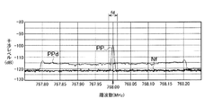
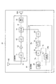
図1〜図3を用いて第1実施形態の発振回路、無線通信装置、及び感度抑圧低減方法を説明する。
図4は、変調経路24aが、内部パルス信号出力部35が出力する内部パルス信号IsのレベルやDCオフセットが基準発振器21に変調をかけるために適切で無い場合に、適切な変調レベルやDCオフセットに調整するレベル調整器51を備える。
10 受信回路
20 発振回路
21 基準発振器
23 電圧制御発振器(VCO)
24,24a 変調経路
30 PLL回路
51 レベル調整器
100 アンテナ
200 報知部
Rs 基準信号
Is 内部パルス信号
Ls ローカル信号
Ns 負帰還信号
Ic 制御電流パルス信号(制御パルス信号)
Claims (9)
- 基準発振器が発振する周波数を基準周波数としてPLL制御を行う発振回路であって、
比較周波数の信号を変調波として前記基準発振器に変調をかける変調経路を備えることを特徴とする発振回路。 - 前記変調波は、位相比較のため基準周波数を分周した信号であることを特徴とする請求項1に記載の発振回路。
- 前記発振回路は、電圧制御発振器の発振周波数をPLL制御により制御する発振回路であって、
前記変調波は、位相比較のため前記電圧制御発振器の発振周波数を分周した信号であることを特徴とする請求項1に記載の発振回路。 - 前記変調経路は、前記変調波のレベルを調整するレベル調整器を備えることを特徴とする請求項1から3のいずれか1項に記載の発振回路。
- 前記レベル調整器は、前記変調波のDCオフセットを調整することを特徴とする請求項4に記載の発振回路。
- 基準発振器が発振する周波数を基準周波数としてPLL制御を行う発振回路を備えた無線通信装置であって、
比較周波数の信号を変調波として前記基準発振器に変調をかける変調経路を備えることを特徴とする無線通信装置。 - 前記変調経路は、前記無線通信装置が受信状態の際に、基準周波数の高調波が受信信号に対して干渉信号となる場合の干渉レベルを低減する変調を行うことを特徴とする請求項6に記載の無線通信装置。
- 基準発振器が発振する周波数を基準周波数としてPLL制御を行う発振回路を備えた無線通信装置の、基準周波数の高調波の干渉による感度抑圧低減方法であって、
比較周波数の信号を変調波として前記基準発振器に変調をかけることを特徴とする感度抑圧低減方法。 - 前記変調は、前記基準周波数の高調波が受信信号に対して干渉信号となる場合の干渉レベルを低減する変調とすることを特徴とする請求項8に記載の感度抑圧低減方法。
Priority Applications (2)
| Application Number | Priority Date | Filing Date | Title |
|---|---|---|---|
| JP2016012955A JP6774594B2 (ja) | 2016-01-27 | 2016-01-27 | 発振回路、無線通信装置、及び感度抑圧低減方法 |
| US15/379,270 US9866361B2 (en) | 2016-01-27 | 2016-12-14 | Radio communication device, oscillation circuit, and sensitivity suppression reduction method |
Applications Claiming Priority (1)
| Application Number | Priority Date | Filing Date | Title |
|---|---|---|---|
| JP2016012955A JP6774594B2 (ja) | 2016-01-27 | 2016-01-27 | 発振回路、無線通信装置、及び感度抑圧低減方法 |
Publications (2)
| Publication Number | Publication Date |
|---|---|
| JP2017135525A true JP2017135525A (ja) | 2017-08-03 |
| JP6774594B2 JP6774594B2 (ja) | 2020-10-28 |
Family
ID=59360908
Family Applications (1)
| Application Number | Title | Priority Date | Filing Date |
|---|---|---|---|
| JP2016012955A Active JP6774594B2 (ja) | 2016-01-27 | 2016-01-27 | 発振回路、無線通信装置、及び感度抑圧低減方法 |
Country Status (2)
| Country | Link |
|---|---|
| US (1) | US9866361B2 (ja) |
| JP (1) | JP6774594B2 (ja) |
Cited By (1)
| Publication number | Priority date | Publication date | Assignee | Title |
|---|---|---|---|---|
| JP7468253B2 (ja) | 2020-08-27 | 2024-04-16 | 株式会社Jvcケンウッド | 受信装置 |
Families Citing this family (2)
| Publication number | Priority date | Publication date | Assignee | Title |
|---|---|---|---|---|
| US10976409B2 (en) * | 2016-11-21 | 2021-04-13 | Electronics And Telecommunications Research Institute | Frequency-modulated continuous wave generator and frequency-modulated continuous wave radar system including the same |
| CN114978211B (zh) * | 2022-05-12 | 2024-06-07 | 维沃移动通信有限公司 | 电子器件保护方法和电子设备 |
Family Cites Families (7)
| Publication number | Priority date | Publication date | Assignee | Title |
|---|---|---|---|---|
| US4652159A (en) * | 1984-05-02 | 1987-03-24 | Kabushiki Kaisha Seiko Epson | Printer |
| DE10108110A1 (de) * | 2001-02-21 | 2002-08-29 | Philips Corp Intellectual Pty | Empfänger und Verfahren zum anfänglichen Synchronisieren eines Empfängers auf die Trägerfrequenz eines gewünschten Kanals |
| WO2009101792A1 (ja) * | 2008-02-12 | 2009-08-20 | Panasonic Corporation | シンセサイザとこれを用いた受信装置 |
| JP2011014961A (ja) | 2009-06-30 | 2011-01-20 | Kenwood Corp | Pll装置及び不要周波数回避方法 |
| US8138841B2 (en) * | 2009-08-19 | 2012-03-20 | City University Of Hong Kong | Apparatus and method for controlling the output phase of a VCO |
| WO2014082155A1 (en) * | 2012-11-29 | 2014-06-05 | Nanowave Technologies Inc. | Low spurious synthesizer circuit and method |
| US8803627B1 (en) * | 2013-12-03 | 2014-08-12 | Innophase Inc. | Wideband direct DCO modulator with in-band compensation |
-
2016
- 2016-01-27 JP JP2016012955A patent/JP6774594B2/ja active Active
- 2016-12-14 US US15/379,270 patent/US9866361B2/en active Active
Cited By (1)
| Publication number | Priority date | Publication date | Assignee | Title |
|---|---|---|---|---|
| JP7468253B2 (ja) | 2020-08-27 | 2024-04-16 | 株式会社Jvcケンウッド | 受信装置 |
Also Published As
| Publication number | Publication date |
|---|---|
| JP6774594B2 (ja) | 2020-10-28 |
| US20170214510A1 (en) | 2017-07-27 |
| US9866361B2 (en) | 2018-01-09 |
Similar Documents
| Publication | Publication Date | Title |
|---|---|---|
| JPH05259935A (ja) | 無線トランシーバ及び周波数制御方法 | |
| HU224302B1 (hu) | Adó-vevő berendezés | |
| US9866361B2 (en) | Radio communication device, oscillation circuit, and sensitivity suppression reduction method | |
| JP3929443B2 (ja) | 2つの周波数帯域で通信可能な無線装置および該無線装置における局部発振信号生成方法 | |
| US20080129406A1 (en) | Direct Wideband Modulation of a Frequency Synthesizer | |
| CN105634410A (zh) | 射频下变频通道装置 | |
| TW200805962A (en) | Radio frequency transceiver and transmission method | |
| JPH1188219A (ja) | 受信機および送受信機 | |
| CN111490782B (zh) | 直接上变频发射机的上变频器及上变频方法 | |
| JP2005304007A (ja) | 位相変調装置、ポーラ変調送信装置、無線送信装置及び無線通信装置 | |
| JP2011151473A (ja) | 角度変調器、送信装置及び無線通信装置 | |
| JP2011014961A (ja) | Pll装置及び不要周波数回避方法 | |
| JP3919343B2 (ja) | 受信機 | |
| JP7846370B2 (ja) | 無線局および周波数誤差補償方法 | |
| JP2005033234A (ja) | 無線機 | |
| EP1091487B1 (en) | Method and apparatus for eliminating self quieter signals generated in synthesiser receivers | |
| JP2017147650A (ja) | 無線通信装置及び電子キーシステム | |
| JP3801493B2 (ja) | 局部発振器を用いた送受信装置 | |
| JP2004349789A (ja) | 周波数変換装置及び周波数変換方法 | |
| JP2015104053A (ja) | 無線機及び基地局 | |
| JP3883743B2 (ja) | 無線装置 | |
| JP4775740B2 (ja) | 受信回路 | |
| JP2018088591A (ja) | 無線通信装置及び局部発振回路の変調度調整方法 | |
| JP2010045504A (ja) | Pll周波数シンセサイザ回路及びその制御方法 | |
| JPH09130434A (ja) | 周波数シンセサイザの変調回路 |
Legal Events
| Date | Code | Title | Description |
|---|---|---|---|
| A621 | Written request for application examination |
Free format text: JAPANESE INTERMEDIATE CODE: A621 Effective date: 20181207 |
|
| A977 | Report on retrieval |
Free format text: JAPANESE INTERMEDIATE CODE: A971007 Effective date: 20190912 |
|
| A131 | Notification of reasons for refusal |
Free format text: JAPANESE INTERMEDIATE CODE: A131 Effective date: 20190924 |
|
| A521 | Request for written amendment filed |
Free format text: JAPANESE INTERMEDIATE CODE: A523 Effective date: 20191115 |
|
| A131 | Notification of reasons for refusal |
Free format text: JAPANESE INTERMEDIATE CODE: A131 Effective date: 20200303 |
|
| A521 | Request for written amendment filed |
Free format text: JAPANESE INTERMEDIATE CODE: A523 Effective date: 20200414 |
|
| TRDD | Decision of grant or rejection written | ||
| A01 | Written decision to grant a patent or to grant a registration (utility model) |
Free format text: JAPANESE INTERMEDIATE CODE: A01 Effective date: 20200901 |
|
| A61 | First payment of annual fees (during grant procedure) |
Free format text: JAPANESE INTERMEDIATE CODE: A61 Effective date: 20200914 |
|
| R150 | Certificate of patent or registration of utility model |
Ref document number: 6774594 Country of ref document: JP Free format text: JAPANESE INTERMEDIATE CODE: R150 |