JP2017138540A - 表示装置 - Google Patents
表示装置 Download PDFInfo
- Publication number
- JP2017138540A JP2017138540A JP2016020679A JP2016020679A JP2017138540A JP 2017138540 A JP2017138540 A JP 2017138540A JP 2016020679 A JP2016020679 A JP 2016020679A JP 2016020679 A JP2016020679 A JP 2016020679A JP 2017138540 A JP2017138540 A JP 2017138540A
- Authority
- JP
- Japan
- Prior art keywords
- liquid crystal
- substrate
- sealing material
- hole
- spacer
- Prior art date
- Legal status (The legal status is an assumption and is not a legal conclusion. Google has not performed a legal analysis and makes no representation as to the accuracy of the status listed.)
- Pending
Links
Images





Classifications
-
- G—PHYSICS
- G02—OPTICS
- G02F—OPTICAL DEVICES OR ARRANGEMENTS FOR THE CONTROL OF LIGHT BY MODIFICATION OF THE OPTICAL PROPERTIES OF THE MEDIA OF THE ELEMENTS INVOLVED THEREIN; NON-LINEAR OPTICS; FREQUENCY-CHANGING OF LIGHT; OPTICAL LOGIC ELEMENTS; OPTICAL ANALOGUE/DIGITAL CONVERTERS
- G02F1/00—Devices or arrangements for the control of the intensity, colour, phase, polarisation or direction of light arriving from an independent light source, e.g. switching, gating or modulating; Non-linear optics
- G02F1/01—Devices or arrangements for the control of the intensity, colour, phase, polarisation or direction of light arriving from an independent light source, e.g. switching, gating or modulating; Non-linear optics for the control of the intensity, phase, polarisation or colour
- G02F1/13—Devices or arrangements for the control of the intensity, colour, phase, polarisation or direction of light arriving from an independent light source, e.g. switching, gating or modulating; Non-linear optics for the control of the intensity, phase, polarisation or colour based on liquid crystals, e.g. single liquid crystal display cells
- G02F1/133—Constructional arrangements; Operation of liquid crystal cells; Circuit arrangements
- G02F1/1333—Constructional arrangements; Manufacturing methods
- G02F1/1339—Gaskets; Spacers; Sealing of cells
- G02F1/13394—Gaskets; Spacers; Sealing of cells spacers regularly patterned on the cell subtrate, e.g. walls, pillars
-
- G—PHYSICS
- G02—OPTICS
- G02F—OPTICAL DEVICES OR ARRANGEMENTS FOR THE CONTROL OF LIGHT BY MODIFICATION OF THE OPTICAL PROPERTIES OF THE MEDIA OF THE ELEMENTS INVOLVED THEREIN; NON-LINEAR OPTICS; FREQUENCY-CHANGING OF LIGHT; OPTICAL LOGIC ELEMENTS; OPTICAL ANALOGUE/DIGITAL CONVERTERS
- G02F1/00—Devices or arrangements for the control of the intensity, colour, phase, polarisation or direction of light arriving from an independent light source, e.g. switching, gating or modulating; Non-linear optics
- G02F1/01—Devices or arrangements for the control of the intensity, colour, phase, polarisation or direction of light arriving from an independent light source, e.g. switching, gating or modulating; Non-linear optics for the control of the intensity, phase, polarisation or colour
- G02F1/13—Devices or arrangements for the control of the intensity, colour, phase, polarisation or direction of light arriving from an independent light source, e.g. switching, gating or modulating; Non-linear optics for the control of the intensity, phase, polarisation or colour based on liquid crystals, e.g. single liquid crystal display cells
- G02F1/133—Constructional arrangements; Operation of liquid crystal cells; Circuit arrangements
- G02F1/1333—Constructional arrangements; Manufacturing methods
- G02F1/1339—Gaskets; Spacers; Sealing of cells
-
- G—PHYSICS
- G02—OPTICS
- G02F—OPTICAL DEVICES OR ARRANGEMENTS FOR THE CONTROL OF LIGHT BY MODIFICATION OF THE OPTICAL PROPERTIES OF THE MEDIA OF THE ELEMENTS INVOLVED THEREIN; NON-LINEAR OPTICS; FREQUENCY-CHANGING OF LIGHT; OPTICAL LOGIC ELEMENTS; OPTICAL ANALOGUE/DIGITAL CONVERTERS
- G02F1/00—Devices or arrangements for the control of the intensity, colour, phase, polarisation or direction of light arriving from an independent light source, e.g. switching, gating or modulating; Non-linear optics
- G02F1/01—Devices or arrangements for the control of the intensity, colour, phase, polarisation or direction of light arriving from an independent light source, e.g. switching, gating or modulating; Non-linear optics for the control of the intensity, phase, polarisation or colour
- G02F1/13—Devices or arrangements for the control of the intensity, colour, phase, polarisation or direction of light arriving from an independent light source, e.g. switching, gating or modulating; Non-linear optics for the control of the intensity, phase, polarisation or colour based on liquid crystals, e.g. single liquid crystal display cells
- G02F1/133—Constructional arrangements; Operation of liquid crystal cells; Circuit arrangements
- G02F1/1333—Constructional arrangements; Manufacturing methods
- G02F1/133345—Insulating layers
-
- G—PHYSICS
- G02—OPTICS
- G02F—OPTICAL DEVICES OR ARRANGEMENTS FOR THE CONTROL OF LIGHT BY MODIFICATION OF THE OPTICAL PROPERTIES OF THE MEDIA OF THE ELEMENTS INVOLVED THEREIN; NON-LINEAR OPTICS; FREQUENCY-CHANGING OF LIGHT; OPTICAL LOGIC ELEMENTS; OPTICAL ANALOGUE/DIGITAL CONVERTERS
- G02F1/00—Devices or arrangements for the control of the intensity, colour, phase, polarisation or direction of light arriving from an independent light source, e.g. switching, gating or modulating; Non-linear optics
- G02F1/01—Devices or arrangements for the control of the intensity, colour, phase, polarisation or direction of light arriving from an independent light source, e.g. switching, gating or modulating; Non-linear optics for the control of the intensity, phase, polarisation or colour
- G02F1/13—Devices or arrangements for the control of the intensity, colour, phase, polarisation or direction of light arriving from an independent light source, e.g. switching, gating or modulating; Non-linear optics for the control of the intensity, phase, polarisation or colour based on liquid crystals, e.g. single liquid crystal display cells
- G02F1/133—Constructional arrangements; Operation of liquid crystal cells; Circuit arrangements
- G02F1/1333—Constructional arrangements; Manufacturing methods
- G02F1/1339—Gaskets; Spacers; Sealing of cells
- G02F1/13396—Spacers having different sizes
-
- G—PHYSICS
- G02—OPTICS
- G02F—OPTICAL DEVICES OR ARRANGEMENTS FOR THE CONTROL OF LIGHT BY MODIFICATION OF THE OPTICAL PROPERTIES OF THE MEDIA OF THE ELEMENTS INVOLVED THEREIN; NON-LINEAR OPTICS; FREQUENCY-CHANGING OF LIGHT; OPTICAL LOGIC ELEMENTS; OPTICAL ANALOGUE/DIGITAL CONVERTERS
- G02F1/00—Devices or arrangements for the control of the intensity, colour, phase, polarisation or direction of light arriving from an independent light source, e.g. switching, gating or modulating; Non-linear optics
- G02F1/01—Devices or arrangements for the control of the intensity, colour, phase, polarisation or direction of light arriving from an independent light source, e.g. switching, gating or modulating; Non-linear optics for the control of the intensity, phase, polarisation or colour
- G02F1/13—Devices or arrangements for the control of the intensity, colour, phase, polarisation or direction of light arriving from an independent light source, e.g. switching, gating or modulating; Non-linear optics for the control of the intensity, phase, polarisation or colour based on liquid crystals, e.g. single liquid crystal display cells
- G02F1/133—Constructional arrangements; Operation of liquid crystal cells; Circuit arrangements
- G02F1/1333—Constructional arrangements; Manufacturing methods
- G02F1/1339—Gaskets; Spacers; Sealing of cells
- G02F1/13398—Spacer materials; Spacer properties
-
- G—PHYSICS
- G02—OPTICS
- G02F—OPTICAL DEVICES OR ARRANGEMENTS FOR THE CONTROL OF LIGHT BY MODIFICATION OF THE OPTICAL PROPERTIES OF THE MEDIA OF THE ELEMENTS INVOLVED THEREIN; NON-LINEAR OPTICS; FREQUENCY-CHANGING OF LIGHT; OPTICAL LOGIC ELEMENTS; OPTICAL ANALOGUE/DIGITAL CONVERTERS
- G02F1/00—Devices or arrangements for the control of the intensity, colour, phase, polarisation or direction of light arriving from an independent light source, e.g. switching, gating or modulating; Non-linear optics
- G02F1/01—Devices or arrangements for the control of the intensity, colour, phase, polarisation or direction of light arriving from an independent light source, e.g. switching, gating or modulating; Non-linear optics for the control of the intensity, phase, polarisation or colour
- G02F1/13—Devices or arrangements for the control of the intensity, colour, phase, polarisation or direction of light arriving from an independent light source, e.g. switching, gating or modulating; Non-linear optics for the control of the intensity, phase, polarisation or colour based on liquid crystals, e.g. single liquid crystal display cells
- G02F1/133—Constructional arrangements; Operation of liquid crystal cells; Circuit arrangements
- G02F1/1333—Constructional arrangements; Manufacturing methods
- G02F1/1341—Filling or closing of cells
-
- G—PHYSICS
- G02—OPTICS
- G02F—OPTICAL DEVICES OR ARRANGEMENTS FOR THE CONTROL OF LIGHT BY MODIFICATION OF THE OPTICAL PROPERTIES OF THE MEDIA OF THE ELEMENTS INVOLVED THEREIN; NON-LINEAR OPTICS; FREQUENCY-CHANGING OF LIGHT; OPTICAL LOGIC ELEMENTS; OPTICAL ANALOGUE/DIGITAL CONVERTERS
- G02F1/00—Devices or arrangements for the control of the intensity, colour, phase, polarisation or direction of light arriving from an independent light source, e.g. switching, gating or modulating; Non-linear optics
- G02F1/01—Devices or arrangements for the control of the intensity, colour, phase, polarisation or direction of light arriving from an independent light source, e.g. switching, gating or modulating; Non-linear optics for the control of the intensity, phase, polarisation or colour
- G02F1/13—Devices or arrangements for the control of the intensity, colour, phase, polarisation or direction of light arriving from an independent light source, e.g. switching, gating or modulating; Non-linear optics for the control of the intensity, phase, polarisation or colour based on liquid crystals, e.g. single liquid crystal display cells
- G02F1/133—Constructional arrangements; Operation of liquid crystal cells; Circuit arrangements
- G02F1/1333—Constructional arrangements; Manufacturing methods
- G02F1/1341—Filling or closing of cells
- G02F1/13415—Drop filling process
-
- G—PHYSICS
- G02—OPTICS
- G02F—OPTICAL DEVICES OR ARRANGEMENTS FOR THE CONTROL OF LIGHT BY MODIFICATION OF THE OPTICAL PROPERTIES OF THE MEDIA OF THE ELEMENTS INVOLVED THEREIN; NON-LINEAR OPTICS; FREQUENCY-CHANGING OF LIGHT; OPTICAL LOGIC ELEMENTS; OPTICAL ANALOGUE/DIGITAL CONVERTERS
- G02F1/00—Devices or arrangements for the control of the intensity, colour, phase, polarisation or direction of light arriving from an independent light source, e.g. switching, gating or modulating; Non-linear optics
- G02F1/01—Devices or arrangements for the control of the intensity, colour, phase, polarisation or direction of light arriving from an independent light source, e.g. switching, gating or modulating; Non-linear optics for the control of the intensity, phase, polarisation or colour
- G02F1/13—Devices or arrangements for the control of the intensity, colour, phase, polarisation or direction of light arriving from an independent light source, e.g. switching, gating or modulating; Non-linear optics for the control of the intensity, phase, polarisation or colour based on liquid crystals, e.g. single liquid crystal display cells
- G02F1/133—Constructional arrangements; Operation of liquid crystal cells; Circuit arrangements
- G02F1/1333—Constructional arrangements; Manufacturing methods
- G02F1/1343—Electrodes
- G02F1/134309—Electrodes characterised by their geometrical arrangement
- G02F1/134363—Electrodes characterised by their geometrical arrangement for applying an electric field parallel to the substrate, i.e. in-plane switching [IPS]
-
- G—PHYSICS
- G02—OPTICS
- G02F—OPTICAL DEVICES OR ARRANGEMENTS FOR THE CONTROL OF LIGHT BY MODIFICATION OF THE OPTICAL PROPERTIES OF THE MEDIA OF THE ELEMENTS INVOLVED THEREIN; NON-LINEAR OPTICS; FREQUENCY-CHANGING OF LIGHT; OPTICAL LOGIC ELEMENTS; OPTICAL ANALOGUE/DIGITAL CONVERTERS
- G02F1/00—Devices or arrangements for the control of the intensity, colour, phase, polarisation or direction of light arriving from an independent light source, e.g. switching, gating or modulating; Non-linear optics
- G02F1/01—Devices or arrangements for the control of the intensity, colour, phase, polarisation or direction of light arriving from an independent light source, e.g. switching, gating or modulating; Non-linear optics for the control of the intensity, phase, polarisation or colour
- G02F1/13—Devices or arrangements for the control of the intensity, colour, phase, polarisation or direction of light arriving from an independent light source, e.g. switching, gating or modulating; Non-linear optics for the control of the intensity, phase, polarisation or colour based on liquid crystals, e.g. single liquid crystal display cells
- G02F1/133—Constructional arrangements; Operation of liquid crystal cells; Circuit arrangements
- G02F1/136—Liquid crystal cells structurally associated with a semi-conducting layer or substrate, e.g. cells forming part of an integrated circuit
- G02F1/1362—Active matrix addressed cells
- G02F1/1368—Active matrix addressed cells in which the switching element is a three-electrode device
-
- G—PHYSICS
- G02—OPTICS
- G02F—OPTICAL DEVICES OR ARRANGEMENTS FOR THE CONTROL OF LIGHT BY MODIFICATION OF THE OPTICAL PROPERTIES OF THE MEDIA OF THE ELEMENTS INVOLVED THEREIN; NON-LINEAR OPTICS; FREQUENCY-CHANGING OF LIGHT; OPTICAL LOGIC ELEMENTS; OPTICAL ANALOGUE/DIGITAL CONVERTERS
- G02F2201/00—Constructional arrangements not provided for in groups G02F1/00 - G02F7/00
- G02F2201/56—Substrates having a particular shape, e.g. non-rectangular
Landscapes
- Physics & Mathematics (AREA)
- Nonlinear Science (AREA)
- Mathematical Physics (AREA)
- Chemical & Material Sciences (AREA)
- Crystallography & Structural Chemistry (AREA)
- General Physics & Mathematics (AREA)
- Optics & Photonics (AREA)
- Liquid Crystal (AREA)
Abstract
Description
Claims (9)
- 第1の基板と、
第2の基板と、
前記第1の基板と前記第2の基板との間に挟持された液晶と、を有する液晶表示装置であって、
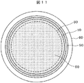
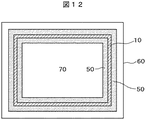
前記第1の基板と前記第2の基板とには孔部が形成され、
前記第1の基板と前記第2の基板とには、表示領域の外側に、第1のシール部が形成され、
前記孔部と前記表示領域との間には第2のシール部が形成され、
前記第2のシール部は、前記液晶側に第1の端部を有し、前記孔部側に第2の端部を有し、
前記第2の端部にはシール材が存在し、
前記第1の端部と前記第2の端部の間に前記孔部を囲むようにスペーサが形成され、前記スペーサは、前記第1の基板と前記第2の基板との間隔を規定していることを特徴とする液晶表示装置。 - 前記スペーサは、前記孔部を囲むように連続して形成されていることを特徴とする請求項1に記載の液晶表示装置。
- 前記スペーサは、前記孔部を囲むように離間して形成されていることを特徴とする請求項1に記載の液晶表示装置。
- 前記スペーサは、平面で視て、屈曲して形成されていることを特徴とする請求項1に記載の液晶表示装置。
- 前記スペーサは、平面で視て、波状に屈曲して形成されていることを特徴とする請求項1に記載の液晶表示装置。
- 前記スペーサは、前記第2のシール部の断面で視て、前記第1の端部と前記第2の端部の間に複数存在していることを特徴とする請求項1に記載の液晶表示装置。
- 前記孔部は、平面で視て、円形であることを特徴とする請求項1に記載の液晶表示装置。
- 前記孔部は、平面で視て、多角形であることを特徴とする請求項1に記載の液晶表示装置。
- 前記第1のシール部は、
前記液晶側に第3の端部を有し、前記液晶側と反対側に第4の端部を有し、
前記第3の端部にはシール材が存在し、
前記第4の端部には土手状スペーサが存在していることを特徴とする請求項1に記載の液晶表示装置。
Priority Applications (4)
| Application Number | Priority Date | Filing Date | Title |
|---|---|---|---|
| JP2016020679A JP2017138540A (ja) | 2016-02-05 | 2016-02-05 | 表示装置 |
| US15/412,514 US10451926B2 (en) | 2016-02-05 | 2017-01-23 | Display device |
| US16/566,983 US10877321B2 (en) | 2016-02-05 | 2019-09-11 | Display device |
| US16/953,573 US11150522B2 (en) | 2016-02-05 | 2020-11-20 | Display device |
Applications Claiming Priority (1)
| Application Number | Priority Date | Filing Date | Title |
|---|---|---|---|
| JP2016020679A JP2017138540A (ja) | 2016-02-05 | 2016-02-05 | 表示装置 |
Publications (1)
| Publication Number | Publication Date |
|---|---|
| JP2017138540A true JP2017138540A (ja) | 2017-08-10 |
Family
ID=59496837
Family Applications (1)
| Application Number | Title | Priority Date | Filing Date |
|---|---|---|---|
| JP2016020679A Pending JP2017138540A (ja) | 2016-02-05 | 2016-02-05 | 表示装置 |
Country Status (2)
| Country | Link |
|---|---|
| US (3) | US10451926B2 (ja) |
| JP (1) | JP2017138540A (ja) |
Cited By (1)
| Publication number | Priority date | Publication date | Assignee | Title |
|---|---|---|---|---|
| CN108957868A (zh) * | 2018-07-27 | 2018-12-07 | 厦门天马微电子有限公司 | 一种显示面板及显示装置 |
Families Citing this family (15)
| Publication number | Priority date | Publication date | Assignee | Title |
|---|---|---|---|---|
| US10802350B2 (en) * | 2016-08-23 | 2020-10-13 | Sharp Kabushiki Kaisha | Display device |
| CN107634072B (zh) * | 2017-10-25 | 2020-04-03 | 厦门天马微电子有限公司 | 阵列基板及显示面板 |
| CN108037609A (zh) * | 2017-11-03 | 2018-05-15 | 惠科股份有限公司 | 一种显示面板及其制作方法 |
| US10756297B2 (en) * | 2018-04-19 | 2020-08-25 | Wuhan China Star Optoelectronics Semiconductor Display Technology Co., Ltd. | Flexible panel, manufacturing method for the same and display device |
| KR102571288B1 (ko) * | 2018-04-27 | 2023-08-28 | 삼성디스플레이 주식회사 | 표시 장치 |
| CN110554530A (zh) * | 2018-06-04 | 2019-12-10 | 鸿富锦精密工业(深圳)有限公司 | 显示面板及显示装置 |
| CN108965511A (zh) * | 2018-06-26 | 2018-12-07 | Oppo广东移动通信有限公司 | 一种显示模组、终端设备及显示模组的布线方法 |
| KR102626939B1 (ko) * | 2018-10-05 | 2024-01-19 | 삼성디스플레이 주식회사 | 표시 장치 |
| CN109307958B (zh) * | 2018-12-14 | 2021-06-29 | 厦门天马微电子有限公司 | 一种显示面板和显示装置 |
| KR102671313B1 (ko) * | 2019-04-23 | 2024-06-03 | 삼성전자주식회사 | 디스플레이 및 그것을 포함하는 전자 장치 |
| KR20230068499A (ko) * | 2021-11-10 | 2023-05-18 | 삼성디스플레이 주식회사 | 표시 장치 및 표시 장치의 제조 방법 |
| US12314520B2 (en) | 2022-03-01 | 2025-05-27 | Apple Inc. | Touch electrode architecture for high-transmittance touch screen |
| KR20230152214A (ko) * | 2022-04-26 | 2023-11-03 | 삼성디스플레이 주식회사 | 색 변환 기판 및 이를 포함하는 표시 장치 |
| US12197668B2 (en) | 2022-09-06 | 2025-01-14 | Apple Inc. | Systems and methods for touch sensing on devices including regions with and without touch electrodes |
| US12487716B2 (en) * | 2022-09-06 | 2025-12-02 | Apple Inc. | Touch electrode architecture for touch screen including touch electrode-free region |
Citations (6)
| Publication number | Priority date | Publication date | Assignee | Title |
|---|---|---|---|---|
| JP2006030440A (ja) * | 2004-07-14 | 2006-02-02 | Seiko Epson Corp | 液晶装置の製造方法、液晶装置、電子機器 |
| JP2009133930A (ja) * | 2007-11-29 | 2009-06-18 | Casio Comput Co Ltd | 液晶表示素子とその製造方法 |
| JP2010139657A (ja) * | 2008-12-10 | 2010-06-24 | Epson Imaging Devices Corp | 液晶パネル、液晶パネルの製造方法、表示装置及び電子機器 |
| JP2015155994A (ja) * | 2014-02-21 | 2015-08-27 | 株式会社ジャパンディスプレイ | 表示装置 |
| JP2015225227A (ja) * | 2014-05-28 | 2015-12-14 | 株式会社ジャパンディスプレイ | 液晶表示装置 |
| JP2016011994A (ja) * | 2014-06-27 | 2016-01-21 | 株式会社ジャパンディスプレイ | 液晶表示装置 |
Family Cites Families (10)
| Publication number | Priority date | Publication date | Assignee | Title |
|---|---|---|---|---|
| JP4609679B2 (ja) * | 2000-07-19 | 2011-01-12 | 日本電気株式会社 | 液晶表示装置 |
| JP2004329692A (ja) * | 2003-05-09 | 2004-11-25 | Hitachi Displays Ltd | 表示装置および遊技機 |
| JP4693479B2 (ja) | 2005-04-28 | 2011-06-01 | セントラル硝子株式会社 | ガラス基板の孔あけドリル |
| CN101713882B (zh) * | 2008-10-01 | 2013-07-17 | 株式会社日立显示器 | 液晶显示装置 |
| US8964159B2 (en) * | 2010-05-18 | 2015-02-24 | Sharp Kabushiki Kaisha | Display device and method for manufacturing the same |
| KR101406129B1 (ko) * | 2012-03-28 | 2014-06-13 | 엘지디스플레이 주식회사 | 디스플레이 장치 |
| KR20140004926A (ko) * | 2012-07-03 | 2014-01-14 | 삼성디스플레이 주식회사 | 표시 장치 |
| WO2014141893A1 (ja) * | 2013-03-15 | 2014-09-18 | シャープ株式会社 | 電子機器 |
| CN103984153B (zh) * | 2013-06-26 | 2017-01-18 | 天马微电子股份有限公司 | 液晶盒及其制造方法 |
| WO2015029704A1 (ja) * | 2013-08-29 | 2015-03-05 | シャープ株式会社 | 表示パネル |
-
2016
- 2016-02-05 JP JP2016020679A patent/JP2017138540A/ja active Pending
-
2017
- 2017-01-23 US US15/412,514 patent/US10451926B2/en active Active
-
2019
- 2019-09-11 US US16/566,983 patent/US10877321B2/en active Active
-
2020
- 2020-11-20 US US16/953,573 patent/US11150522B2/en active Active
Patent Citations (6)
| Publication number | Priority date | Publication date | Assignee | Title |
|---|---|---|---|---|
| JP2006030440A (ja) * | 2004-07-14 | 2006-02-02 | Seiko Epson Corp | 液晶装置の製造方法、液晶装置、電子機器 |
| JP2009133930A (ja) * | 2007-11-29 | 2009-06-18 | Casio Comput Co Ltd | 液晶表示素子とその製造方法 |
| JP2010139657A (ja) * | 2008-12-10 | 2010-06-24 | Epson Imaging Devices Corp | 液晶パネル、液晶パネルの製造方法、表示装置及び電子機器 |
| JP2015155994A (ja) * | 2014-02-21 | 2015-08-27 | 株式会社ジャパンディスプレイ | 表示装置 |
| JP2015225227A (ja) * | 2014-05-28 | 2015-12-14 | 株式会社ジャパンディスプレイ | 液晶表示装置 |
| JP2016011994A (ja) * | 2014-06-27 | 2016-01-21 | 株式会社ジャパンディスプレイ | 液晶表示装置 |
Cited By (1)
| Publication number | Priority date | Publication date | Assignee | Title |
|---|---|---|---|---|
| CN108957868A (zh) * | 2018-07-27 | 2018-12-07 | 厦门天马微电子有限公司 | 一种显示面板及显示装置 |
Also Published As
| Publication number | Publication date |
|---|---|
| US10877321B2 (en) | 2020-12-29 |
| US20200004074A1 (en) | 2020-01-02 |
| US11150522B2 (en) | 2021-10-19 |
| US20210088826A1 (en) | 2021-03-25 |
| US10451926B2 (en) | 2019-10-22 |
| US20170227804A1 (en) | 2017-08-10 |
Similar Documents
| Publication | Publication Date | Title |
|---|---|---|
| US11150522B2 (en) | Display device | |
| JP6502638B2 (ja) | 液晶表示装置およびマザー基板 | |
| US20200348548A1 (en) | Liquid crystal display device | |
| KR102135931B1 (ko) | 간격 스페이서와 누름 스페이서를 구비한 액정 표시장치 | |
| JP2014206596A (ja) | 液晶表示装置及びその製造方法 | |
| JP2017111290A (ja) | 液晶表示装置 | |
| JP2009150916A (ja) | 液晶表示装置 | |
| JP2009116214A (ja) | 液晶パネル及びその製造方法 | |
| JP5266736B2 (ja) | 液晶表示素子とその製造方法 | |
| WO2008072464A1 (ja) | 液晶表示素子 | |
| JP2009109658A (ja) | 液晶表示装置及びその製造方法 | |
| JP2008151969A (ja) | 液晶表示パネルおよびこれを備える電子機器並びに液晶表示パネルの製造方法 | |
| JP5610411B2 (ja) | 液晶表示装置及びその製造方法 | |
| US10031376B2 (en) | Liquid crystal display device | |
| JP2017122790A (ja) | 液晶表示装置 | |
| US8064031B2 (en) | Liquid crystal display device | |
| US20130010250A1 (en) | Liquid crystal display device and manufacturing method thereof | |
| US11022846B2 (en) | Substrate for display device and display device | |
| JP2019091098A (ja) | 液晶表示装置 | |
| JP2008096836A (ja) | 液晶表示パネルの製造方法、および液晶表示パネル | |
| US9128330B2 (en) | Liquid crystal display device and method of manufacturing the same | |
| JP2008003194A (ja) | 基板装置および表示素子の製造方法 | |
| JP2008145634A (ja) | 液晶表示装置 | |
| JP7183320B2 (ja) | 液晶表示装置 | |
| JP2008233242A (ja) | 液晶表示装置、及び液晶表示装置の製造方法 |
Legal Events
| Date | Code | Title | Description |
|---|---|---|---|
| A621 | Written request for application examination |
Free format text: JAPANESE INTERMEDIATE CODE: A621 Effective date: 20181221 |
|
| A977 | Report on retrieval |
Free format text: JAPANESE INTERMEDIATE CODE: A971007 Effective date: 20191023 |
|
| A131 | Notification of reasons for refusal |
Free format text: JAPANESE INTERMEDIATE CODE: A131 Effective date: 20191029 |
|
| A521 | Request for written amendment filed |
Free format text: JAPANESE INTERMEDIATE CODE: A523 Effective date: 20191223 |
|
| A131 | Notification of reasons for refusal |
Free format text: JAPANESE INTERMEDIATE CODE: A131 Effective date: 20200324 |
|
| A521 | Request for written amendment filed |
Free format text: JAPANESE INTERMEDIATE CODE: A523 Effective date: 20200515 |
|
| A02 | Decision of refusal |
Free format text: JAPANESE INTERMEDIATE CODE: A02 Effective date: 20201020 |