JP2017141482A - Functional parts, methods for producing functional parts - Google Patents
Functional parts, methods for producing functional parts Download PDFInfo
- Publication number
- JP2017141482A JP2017141482A JP2016021766A JP2016021766A JP2017141482A JP 2017141482 A JP2017141482 A JP 2017141482A JP 2016021766 A JP2016021766 A JP 2016021766A JP 2016021766 A JP2016021766 A JP 2016021766A JP 2017141482 A JP2017141482 A JP 2017141482A
- Authority
- JP
- Japan
- Prior art keywords
- conductive layer
- adhesion layer
- electroforming
- functional component
- glass substrate
- Prior art date
- Legal status (The legal status is an assumption and is not a legal conclusion. Google has not performed a legal analysis and makes no representation as to the accuracy of the status listed.)
- Granted
Links
Images


Landscapes
- Physical Vapour Deposition (AREA)
Abstract
【課題】電極膜とガラス基板との密着性に優れ、かつ導電層の耐酸性にも優れた機能部品、およびその製造方法を提供する。【解決手段】ガラス基板と、該ガラス基板上に形成されてなる、クロム酸化物を主成分とした密着層、および該密着層上に形成されてなる、少なくとも主成分がクロムであり、8atom%以上、38atom%以下の濃度範囲の窒素を含む導電層を少なくとも有する電極膜を備えた。【選択図】図1The present invention provides a functional component that has excellent adhesion between an electrode film and a glass substrate and also has an excellent acid resistance of a conductive layer, and a method for manufacturing the same. [Solution] A glass substrate, an adhesion layer formed on the glass substrate and containing chromium oxide as a main component, and an adhesion layer formed on the adhesion layer, in which at least the main component is chromium, and the content is 8 atom%. As described above, an electrode film having at least a conductive layer containing nitrogen in a concentration range of 38 atom % or less is provided. [Selection diagram] Figure 1
Description
本発明は、電鋳によるメタルマスクの製造に用いる電鋳用マスク原版に好適な機能部品、およびその製造方法に関する。 The present invention relates to a functional component suitable for an electroforming mask master used for manufacturing a metal mask by electroforming, and a manufacturing method thereof.
例えば、有機EL(Electro Luminescence:エレクトロルミネッセンス )ディスプレイ等において、高精度で微細なパターン成膜を行うための蒸着用マスクとして、メタルマスクが用いられている。こうしたメタルマスクの製造方法として、一般的に、金属箔にエッチングを行うことによって製造する方法と、電鋳によって製造する方法とが知られている。 For example, in an organic EL (Electro Luminescence) display or the like, a metal mask is used as a vapor deposition mask for forming a fine pattern with high accuracy. As a method for manufacturing such a metal mask, a method of manufacturing a metal foil by etching and a method of manufacturing by electroforming are generally known.
このうち、金属箔を用いて製造したメタルマスクは、材料となる金属箔の厚みを薄くすることが困難である。このため、蒸着用メタルマスクとして用いた際に金属箔の厚みが厚いために影が生じやすく、微細なパターン成膜を行うことが困難であった。 Among these, it is difficult to reduce the thickness of the metal foil used as a material for the metal mask manufactured using the metal foil. For this reason, when it used as a metal mask for vapor deposition, since the thickness of metal foil was thick, it was easy to produce a shadow and it was difficult to form a fine pattern film.
一方、電鋳によるメタルマスクの製造は、電気メッキによる薄膜形成のため、マスク材膜の厚みを薄くすることが容易である。電鋳によるメタルマスクの製造では、ガラス基板上に所望のパターンを備えた電極膜が形成された電鋳用マスク原版が用いられている。こうした電鋳用マスク原版にメッキを行って所望のパターンのメッキ膜を形成し、このメッキ膜を電鋳用マスク原版から引き剥がすことにより、メタルマスクを製造する(例えば、特許文献1を参照)。 On the other hand, in the production of a metal mask by electroforming, it is easy to reduce the thickness of the mask material film because a thin film is formed by electroplating. In the production of a metal mask by electroforming, an electroforming mask original plate in which an electrode film having a desired pattern is formed on a glass substrate is used. A metal mask is manufactured by plating such an electroforming mask original plate to form a plating film having a desired pattern and peeling the plating film from the electroforming mask original plate (see, for example, Patent Document 1). .
しかしながら、従来、こうした電鋳用マスク原版は、ガラス基板と電極膜との密着性が十分でなかったために、1回ないし数回のメタルマスクの形成でガラス基板から電極膜が剥離してしまい、耐久性に課題があった。 However, conventionally, such an electroforming mask original plate has insufficient adhesion between the glass substrate and the electrode film, so that the electrode film is peeled off from the glass substrate by forming the metal mask once or several times. There was a problem with durability.
また、近年、従来のニッケル電鋳マスクに代えて、高精度なメタルマスクの製造に好適な、低熱膨張金属であるNi−Fe合金を用いた電鋳マスクが開発されつつある(例えば、非特許文献1を参照)。
しかしながら、従来のニッケル電鋳ではメッキ液がpH4程度であったに対して、Ni−Fe合金を用いた電鋳ではメッキ液がpH2.3と酸性が強くなる。このため、従来の電鋳用マスク原版では、クロムを主成分とした電極膜の耐酸性が不足し、電鋳時にメッキ液による腐食でパターン欠けが生じやすいという課題があった。
In recent years, instead of the conventional nickel electroforming mask, an electroforming mask using a Ni—Fe alloy, which is a low thermal expansion metal, suitable for manufacturing a highly accurate metal mask has been developed (for example, non-patent). Reference 1).
However, in the conventional nickel electroforming, the plating solution has a pH of about 4, whereas in the electroforming using a Ni—Fe alloy, the plating solution has a pH of 2.3 and becomes more acidic. For this reason, the conventional electroforming mask original plate has a problem that the acid resistance of the electrode film mainly composed of chromium is insufficient, and pattern chipping is likely to occur due to corrosion by a plating solution during electroforming.
本発明は、上述の事情に鑑みてなされたものであり、電極膜とガラス基板との密着性に優れ、かつ電極膜の耐酸性にも優れた機能部品、およびその製造方法を提供するものである。 This invention is made | formed in view of the above-mentioned situation, and provides the functional component which was excellent in the adhesiveness of an electrode film and a glass substrate, and was excellent also in the acid resistance of an electrode film, and its manufacturing method. is there.
本発明の機能部品は、ガラス基板と、該ガラス基板上に形成されてなる、クロム酸化物を主成分とした密着層、および該密着層上に形成されてなる、少なくとも主成分がクロムであり、8atom%以上、38atom%以下の濃度範囲の窒素を含む導電層を少なくとも有する電極膜を備えたことを特徴とする。 The functional component of the present invention includes a glass substrate, an adhesion layer formed on the glass substrate, mainly composed of chromium oxide, and at least a major component formed on the adhesion layer. And an electrode film having at least a conductive layer containing nitrogen in a concentration range of 8 atom% or more and 38 atom% or less.
本発明の機能部品によれば、導電層とガラス基板との間にクロム酸化物を主成分とした密着層を形成することによって、電極膜とガラス基板との密着性を大幅に向上させることができる。これによって、例えば、機能部品を電鋳用マスク原版にして電鋳によってメタルマスクを形成した際に、メッキ形成したメタルマスクを機能部品から剥離させても、電極膜がガラス基板から容易に剥脱したり、一部が損傷する懸念が無い。これにより、機能部品を電鋳用マスク原版に用いた際に、複数回繰り返しメタルマスクを製造するために充分な強度を備えた機能部品を実現できる。 According to the functional component of the present invention, the adhesion between the electrode film and the glass substrate can be greatly improved by forming an adhesion layer mainly composed of chromium oxide between the conductive layer and the glass substrate. it can. Thus, for example, when a functional part is used as an electroforming mask master and a metal mask is formed by electroforming, the electrode film is easily peeled off from the glass substrate even if the plated metal mask is peeled off from the functional part. There is no concern that some will be damaged. Thereby, when a functional component is used for an electroforming mask master, a functional component having sufficient strength to repeatedly manufacture a metal mask can be realized.
また、本発明の機能部品によれば、導電層を、少なくとも主成分がクロムであり、8atom%以上、38atom%以下の濃度範囲の窒素を含む材料で構成することによって、導電層の耐酸性を大幅に向上させることができる。こうした導電層の耐酸性の向上によって、例えば、Ni−Fe合金を用いた電鋳に用いるpH2.3といった酸性度の高いメッキ液に対しても、導電層の腐蝕を充分に抑制することができる。よって、高精度なメタルマスクの製造に好適な、低熱膨張金属であるNi−Fe合金を用いた電鋳を行うことが可能になる。 Further, according to the functional component of the present invention, the conductive layer is made of a material containing at least a main component of chromium and containing nitrogen in a concentration range of 8 atom% or more and 38 atom% or less. It can be greatly improved. By improving the acid resistance of the conductive layer, the corrosion of the conductive layer can be sufficiently suppressed even for a plating solution having a high acidity such as pH 2.3 used for electroforming using a Ni—Fe alloy. . Therefore, it becomes possible to perform electroforming using a Ni—Fe alloy which is a low thermal expansion metal suitable for manufacturing a highly accurate metal mask.
前記導電層は、炭素を更に含むことを特徴とする。
また、前記炭素は、3atom%以上、18atom%以下の濃度範囲で前記導電層に含まれることを特徴とする。
また、前記密着層は、積層方向に沿った厚みが10nm以上、50nm以下の範囲であることを特徴とする。
また、前記導電層は、抵抗率が0.8×10⁻⁶Ω・m以上、2.5×10⁻⁶Ω・m以下の範囲であることを特徴とする。
The conductive layer further includes carbon.
Further, the carbon is included in the conductive layer in a concentration range of 3 atom% or more and 18 atom% or less.
Further, the adhesion layer has a thickness in the range of 10 nm or more and 50 nm or less along the stacking direction.
The conductive layer has a resistivity in a range of 0.8 × 10 −6 Ω · m to 2.5 × 10 −6 Ω · m.
また、前記導電層は、積層方向に沿った厚みが100nm以上、500nm以下の範囲であることを特徴とする。 The conductive layer has a thickness in the range of 100 nm or more and 500 nm or less along the stacking direction.
本発明の機能部品の製造方法は、ガラス基板上に、クロム酸化物を主成分とした密着層を形成する工程と、該密着層上に、少なくとも主成分がクロムであり、8atom%以上、38atom%以下の濃度範囲の窒素を含む導電層を形成する工程と、を備えたことを特徴とする。 The method for producing a functional component according to the present invention includes a step of forming an adhesion layer containing chromium oxide as a main component on a glass substrate, and at least a main component is chromium on the adhesion layer, and is at least 8 atom% and 38 atom. And a step of forming a conductive layer containing nitrogen in a concentration range of not more than%.
本発明の機能部品の製造方法によれば、導電層とガラス基板との間にクロム酸化物を主成分とした密着層を形成することによって、電極膜とガラス基板との密着性が大幅に向上するので、例えば、機能部品を電鋳用マスク原版にして電鋳によってメタルマスクを形成した際に、メッキ形成したメタルマスクを機能部品から剥離させても、電極膜がガラス基板から容易に剥脱したり、一部が損傷する懸念が無い。これにより、高精度なメタルマスクを容易に製造することができる。 According to the method for producing a functional component of the present invention, the adhesion between the electrode film and the glass substrate is greatly improved by forming an adhesion layer mainly composed of chromium oxide between the conductive layer and the glass substrate. Therefore, for example, when a functional part is used as an electroforming mask master and a metal mask is formed by electroforming, the electrode film is easily peeled off from the glass substrate even if the plated metal mask is peeled off from the functional part. There is no concern that some will be damaged. Thereby, a highly accurate metal mask can be manufactured easily.
また、本発明の機能部品の製造方法によれば、導電層を、少なくとも主成分がクロムであり、8atom%以上、38atom%以下の濃度範囲の窒素を含む材料で構成することによって、導電層の耐酸性が大幅に向上し、例えば、Ni−Fe合金を用いた電鋳に用いるpH2.3といった酸性度の高いメッキ液に対しても、導電層の腐蝕を充分に抑制することができる。よって、高精度なメタルマスクの製造に好適な、低熱膨張金属であるNi−Fe合金を用いた電鋳を行うことが可能になる。 According to the method for manufacturing a functional component of the present invention, the conductive layer is made of a material containing at least a main component of chromium and containing nitrogen in a concentration range of 8 atom% or more and 38 atom% or less. The acid resistance is greatly improved, and the corrosion of the conductive layer can be sufficiently suppressed even for a plating solution having a high acidity such as pH 2.3 used for electroforming using a Ni—Fe alloy. Therefore, it becomes possible to perform electroforming using a Ni—Fe alloy which is a low thermal expansion metal suitable for manufacturing a highly accurate metal mask.
前記密着層および前記導電層を少なくとも備えた電極膜の表面にクロム用エッチャントを用いてエッチングを施して、該電極膜に所定の電極パターンを形成する工程をさらに有することを特徴とする。 The method further includes the step of etching the surface of the electrode film provided with at least the adhesion layer and the conductive layer using a chromium etchant to form a predetermined electrode pattern on the electrode film.
前記密着層および前記導電層を少なくとも備えた電極膜の表面に所定のパターンを有する不導体膜を形成する工程をさらに有することを特徴とする。 The method further includes the step of forming a nonconductive film having a predetermined pattern on the surface of the electrode film having at least the adhesion layer and the conductive layer.
本発明によれば、電極膜とガラス基板との密着性に優れ、かつ導電層の耐酸性にも優れた機能部品、およびその製造方法を提供することができる。 ADVANTAGE OF THE INVENTION According to this invention, the functional component which was excellent in the adhesiveness of an electrode film and a glass substrate, and was excellent also in the acid resistance of a conductive layer, and its manufacturing method can be provided.
以下、図面を参照して、本発明の機能部品、および機能部品の製造方法について説明する。なお、以下に示す各実施形態は、発明の趣旨をより良く理解させるために具体的に説明するものであり、特に指定のない限り、本発明を限定するものではない。また、以下の説明で用いる図面は、本発明の特徴をわかりやすくするために、便宜上、要部となる部分を拡大して示している場合があり、各構成要素の寸法比率などが実際と同じであるとは限らない。 Hereinafter, the functional component of the present invention and the method of manufacturing the functional component will be described with reference to the drawings. Each embodiment described below is specifically described for better understanding of the gist of the invention, and does not limit the present invention unless otherwise specified. In addition, in the drawings used in the following description, in order to make the features of the present invention easier to understand, there is a case where a main part is shown in an enlarged manner for convenience, and the dimensional ratio of each component is the same as the actual one. Not necessarily.
(機能部品)
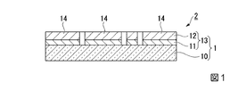
図1は、本発明の実施形態に係る機能部品を示す要部拡大断面図である。
機能部品1は、電鋳によってメタルマスクを製造する際に用いる電鋳用マスク原版に好適な部品であり、ガラス基板10と、このガラス基板10上には、密着層11と、この密着層11上に形成された導電層12とを有する電極膜13が形成されている。
(functional parts)
FIG. 1 is an enlarged cross-sectional view showing a main part of a functional component according to an embodiment of the present invention.
The
ガラス基板10の構成材料は、特に限定されるものではないが、例えば、無アルカリガラス、石英ガラス、ホウ珪酸ガラス(Schott製のテンパックスフロート)、ソーダライムガラス、白板等、また純粋なSiO2に近いガラスからSiO2以外の不純物(添加物)を多く含むガラスなど、種々のガラスが挙げられる。本実施形態では、ガラス基板10の構成材料として、ソーダライムガラスを用いた。
The constituent material of the
密着層11は、その上に重ねて形成される導電層12とガラス基板10との密着性を高めるために、密着層11と導電層12との間に形成される膜である。こうした密着層11の構成材料は、クロム酸化物を主成分としている。更に、クロム酸化物に加えて、クロム炭化物、クロム窒化物を含むことがより好ましい。
The
密着層11に含まれる酸素は、20atom%以上、50atom%以下の濃度範囲である。
The oxygen contained in the
こうした密着層11は、積層方向に沿った厚みが10nm以上、50nm以下の範囲になるように形成される。更に好ましくは、厚みが10nm以上、30nm以下の範囲になるように形成される。密着層11の厚みが10nm未満であると、ガラス基板10の成分、例えばナトリウム、カリウム、マグネシウム、カルシウムなどのアルカリ成分が導電層12に達して、導電層12の特性を劣化させる虞がある。こうした導電層12とガラス基板10との間のバリア性の面から、密着層11の厚みが10nm以上であることが好ましい。なお、ガラス基板10として、アルカリ成分を含まない無アルカリガラス、ホウ珪酸ガラス、石英ガラス等を用いれば、密着層11の厚みを更に薄くすることも可能である。
The
密着層11の厚みが50nmを超えると、成膜に時間がかかり、また、膜強度の面からも好ましくない。よって、密着層11の厚みは、10nm以上、50nm以下の範囲になるように形成される。
When the thickness of the
導電層12は、少なくとも主成分がクロムであり、8atom%以上、38atom%以下の濃度範囲の窒素を含む材料で構成されている。更に好ましくは、導電層12は、14atom%以上、38atom%以下の濃度範囲の窒素を含む。
The
導電層12として、主成分のクロムに対して上述した濃度範囲の窒素を含有させることによって、耐酸性を高めることが可能になる。例えば、電鋳によってメタルマスクを製造する際に、従来のようにニッケルによる電鋳よりもpHが低いNi−Fe合金用のメッキ液に対しても、高い耐酸性を得ることができ、Ni−Fe合金によるメタルマスクの製造を可能にする。
By including nitrogen in the above-described concentration range with respect to the main component chromium as the
また、導電層12の積層方向に沿った厚みは、100nm以上、500nm以下の範囲にすることが好ましい。導電層12の厚みが100nm未満であると、電鋳を行った際に電気抵抗が高まり、メタルマスクの製造に要する時間が長くなる懸念がある。一方、導電層12の厚みが500nmを超えると、導電層12の成膜に時間が掛かり、機能部品1の製造コストが上昇する虞がある。
Moreover, it is preferable to make the thickness along the lamination direction of the
また、導電層12は、抵抗率が0.8×10⁻⁶Ω・m以上、2.5×10⁻⁶Ω・m以下の範囲にすることが好ましい。導電層12の抵抗率を2.5×10⁻⁶Ω・m以下にすることによって、機能部品10を電鋳用マスク原版として用いた際に、電鋳時に電極膜12上に効率的にメッキ膜(メタルマスク)を形成することができる。
The
導電層12は、主成分のクロム、および添加元素である窒素に加えて、更に炭素を含有することが好ましい。導電層12の炭素含有濃度は、3atom%以上、18atom%以下の濃度範囲であることが好ましい。
導電層12に炭素を含有させることによって、導電層12の耐酸性を更に高めることが可能になる。
The
By containing carbon in the
こうした導電層12および密着層11を有する電極膜13からなる機能部品1の一部に、所望のメタルマスク形状を象った開口部を設けることによって、所定形状の電極パターン14を備えた電極パターン付きの機能部品2が形成される。電極パターン14は、機能部品1を電鋳によってメタルマスクを製造する際に用いる電鋳用マスク原版として用いた際に、製造するメタルマスクの形状を象ったものであり、後述する機能部品の製造方法におけるエッチング工程において、機能部品1の電極膜13をエッチングすることによって形成される。
An electrode pattern provided with an
以上のような構成の本発明の機能部品1によれば、導電層12とガラス基板10との間にクロム酸化物を主成分とした密着層11を形成することによって、こうした機能部品1を電鋳用マスク原版として用いた際に、導電層12および密着層11を有する電極膜13とガラス基板10との密着性を大幅に向上させることができる。
According to the
これによって、例えば、機能部品1を電鋳用マスク原版にして電鋳によってメタルマスクを形成した際に、メッキ形成したメタルマスクを機能部品1から剥離させても、導電層12および密着層11を有する電極膜13がガラス基板10から容易に剥脱したり、一部が損傷する懸念が無い。これにより、機能部品1を電鋳用マスク原版に用いた際に、複数回繰り返しメタルマスクを製造するために充分な強度を備えた機能部品1を実現できる。
As a result, for example, when the metal mask is formed by electroforming using the
また、本発明の機能部品1によれば、導電層12を、少なくとも主成分がクロムであり、8atom%以上、38atom%以下の濃度範囲の窒素を含む材料で構成することによって、導電層12の耐酸性を大幅に向上させることができる。
According to the
こうした導電層12の耐酸性の向上によって、例えば、Ni−Fe合金を用いた電鋳に用いるpH2.3といった酸性度の高いメッキ液に対しても、導電層12の腐蝕を充分に抑制することができる。よって、高精度なメタルマスクの製造に好適な、低熱膨張金属であるNi−Fe合金を用いた電鋳を行うことが可能になる。
By improving the acid resistance of the
(機能部品の製造方法)
次に、上述した構成の機能部品の製造方法を説明する。
図2は、本発明の機能部品の製造方法、およびこれを用いたメタルマスクの製造方法を段階的に説明したフローチャートである。また、図3は、本発明の機能部品の製造方法を段階的に説明した要部拡大断面図である。
機能部品1を製造する際には、まず、ガラス基板10を用意する。ガラス基板10としては、例えば、例えば、無アルカリガラス、石英ガラス、ホウ珪酸ガラス(Schott製のテンパックスフロート)、ソーダライムガラス、白板等、また純粋なSiO2に近いガラスからSiO2以外の不純物(添加物)を多く含むガラスなどを用いることができる。本実施形態では、ガラス基板10の構成材料として、ソーダライムガラスを用いた。
(Functional parts manufacturing method)
Next, a method for manufacturing the functional component having the above-described configuration will be described.
FIG. 2 is a flowchart illustrating step by step a method for manufacturing a functional component according to the present invention and a method for manufacturing a metal mask using the method. FIG. 3 is an enlarged cross-sectional view of a main part illustrating the method for manufacturing a functional component according to the present invention step by step.
When manufacturing the
そして、図3(a)に示すように、前処理として、ガラス基板10に密着層11を形成する被加工面10aを研磨して、被加工面10aを平滑化させる(前処理工程S1)。前処理工程S1では、例えば、研磨パッドPと、酸化セリウムを主成分とする研磨液とを用いてガラス基板10の被加工面10aを研磨する。この研磨工程は任意の回数行うことができる。更に、研磨処理後のガラス基板10を公知の洗浄方法を用いて洗浄し、基板面に付着した研磨液などを除去する。ガラス基板10の洗浄方法としては、洗剤を用いて洗浄した後、純水洗浄を施すのが一般的である。
And as shown to Fig.3 (a), the to-
次に、図3(b)に示すように、前処理を施したガラス基板10の被加工面10aに、密着層11を形成する(密着層形成工程S2)。密着層11は、クロム酸化物を主成分としている。更に、クロム酸化物に加えて、クロム炭化物、クロム窒化物を含むことも好ましい。
Next, as shown in FIG.3 (b), the contact |
密着層11に含まれる酸素は、20atom%以上、50atom%以下の濃度範囲である。
また、密着層11は、積層方向に沿った厚みが10nm以上、50nm以下の範囲になるように形成する。
The oxygen contained in the
The
こうした密着層形成工程S2における密着層11の成膜方法としては、量産性等を考慮して、スパッタリング法を用いることが好ましい。この場合、スパッタガスとしては、アルゴンガス、窒素ガス及び二酸化炭素ガスの混合ガスを用いることが好ましく、所望の膜厚、膜の密着性が得られるように、流量比を設定できる。特に膜中の窒素濃度が条規の範囲となるように窒素ガス流量等の条件を設定する。なお、スパッタリング装置としては、公知の構造を有するものを用いることができる。
こうしたアルゴンガス、窒素ガス及び二酸化炭素ガスを用いたスパッタリング法によって、ガラス基板10の被加工面10aに、クロム酸化物を主成分とした密着層11を形成することができる。
As a method for forming the
By the sputtering method using such argon gas, nitrogen gas, and carbon dioxide gas, the
次に、図3(c)に示すように、密着層11の上に、導電層12を形成する(導電層形成工程S3)。これにより、導電層12および密着層11を有する電極膜13がガラス基板10上に形成された機能部品1が得られる。
導電層12は、少なくとも主成分がクロムであり、8atom%以上、38atom%以下の濃度範囲の窒素を含む材料で構成されている。こうした導電層形成工程S3における導電層12の成膜方法としては、量産性等を考慮して、スパッタリング法を用いることが好ましい。この場合、スパッタガスとしては、アルゴンガス、および窒素ガスの混合ガスを用いることが好ましく、所望の膜厚、膜の密着性が得られるように、流量比を設定できる。特に膜中の窒素濃度が条規の範囲となるように窒素ガス流量等の条件を設定する。なお、スパッタリング装置としては、公知の構造を有するものを用いることができる。
Next, as shown in FIG. 3C, a
The
導電層12は、積層方向に沿った厚みが100nm以上、500nm以下の範囲になるように成膜することが好ましい。こうした導電層12は、電鋳によるメタルマスクの形成を容易にするために、抵抗率が0.8×10⁻⁶Ω・m以上、2.5×10⁻⁶Ω・m以下の範囲にされる。
The
導電層12は、主成分のクロム、および添加元素である窒素に加えて、更に炭素を含有することが好ましい。導電層12の炭素含有濃度は、3atom%以上、18atom%以下の濃度範囲であることが好ましい。導電層12に炭素を含有させるには、導電層11をスパッタリング法によって形成する際に用いるスパッタガスとしては、アルゴンガス、窒素ガスに加えて、炭素源として二酸化炭素ガスを加えることによって実現できる。
The
次に、図3(d)に示すように、導電層12および密着層11を有する電極膜13を備えた機能部品1の上に、レジストパターン15を形成する(レジストパターン形成工程S4)。こうしたレジストパターン形成工程S4におけるレジストパターン15の形成方法としては、電極膜13上にレジストを一様に塗布し、これを露光、現像処理することで、開口部15aを有するレジストパターン15を形成する。レジストパターン15の形状は、電鋳によって製造するメタルマスクの形状を象ったものであればよい。
Next, as shown in FIG. 3D, a resist
次に、図3(e)に示すように、レジストパターン15をエッチングマスクとして、湿式エッチング処理により電極膜13に所定の電極パターン14を形成する(エッチング工程S5)。
Next, as shown in FIG. 3E, a
エッチング工程S5では、クロム用エッチング液、例えば、硝酸セリウムアンモニウムを主成分とするエッチング液を用いて、レジストパターン15の開口部15aで露呈された部分の電極膜13をエッチングすることによって、電極膜13が所定の電極パターン14になるように形成する。
In the etching step S5, the
そして、最後に、図3(f)に示すように、電極膜13上のレジストパターン15を、公知の剥離方法を用いて剥離すれば(レジスト除去工程S6)、導電性の電極膜13に所定の電極パターン14が形成され、かつこの導電層12が密着層11を介してガラス基板10に強固に接合された機能部品1を備えた電極パターン付きの機能部品2を得ることができる。
Finally, as shown in FIG. 3F, if the resist
こうした電極パターン付きの機能部品2を、電鋳によってメタルマスクを製造する際の電鋳用マスク原版として用い、メタルマスクを製造する際には、図4(a)に示すように、鉄板およびニッケル板または、Ni−Fe金属板Sを陽極に、また、電極パターン付きの機能部品2の電極膜13を陰極にして、電鋳(電気めっき)を行う(電鋳工程S11)。電鋳に用いる電解液(メッキ液)Wとしては、例えば、NiSO4、NiCl2、H3BO3、FeSO4、マロン酸などを主成分とした、pH2.3程度の酸性度の高いNi−Feメッキ液を用いる。
When such a
このような電鋳工程S11において、本発明の機能部品1(電極パターン付きの機能部品2)のように、導電層12を、少なくとも主成分がクロムであり、8atom%以上、38atom%以下の濃度範囲の窒素を含む材料で構成することによって、導電層12の耐酸性を大幅に向上し、pH2.3程度の酸性度の高いNi−Feメッキ液を用いても、導電層12が腐食される懸念が無い。
In such an electroforming step S11, as in the functional component 1 (
こうした電鋳工程S11で所定時間、所定の電流を流すことによって、図4(a)に示すように、電極パターン付きの機能部品2の電極膜13上に、Ni−Fe金属メッキ層であるメタルマスクMが形成される。
By supplying a predetermined current for a predetermined time in the electroforming step S11, as shown in FIG. 4A, a metal that is a Ni—Fe metal plating layer is formed on the
そして、図4(b)に示すように、形成されたメタルマスクMを電極膜13から剥離させることによって、電極膜13に形成された電極パターン14が転写された貫通穴VをもつメタルマスクMを得ることができる(マスク剥離工程S12)。また、メタルマスクMを剥離後の電極パターン付きの機能部品2は、再び電鋳用マスク原版として、メタルマスクMの電鋳による製造に繰り返し用いることができる。
Then, as shown in FIG. 4B, the formed metal mask M is peeled off from the
導電層12とガラス基板10との間にクロム酸化物を主成分とした密着層11を形成した機能部品1(電極パターン付きの機能部品2)を用いることによって、電極膜13とガラス基板10との密着性が大幅に向上する。これによって、機能部品1を電鋳用マスク原版にして電鋳によってメタルマスクを形成した際に、メッキ形成したメタルマスクを機能部品1から剥離させても、電極膜13がガラス基板10から容易に剥脱したり、一部が損傷する懸念が無い。よって、複数回繰り返しメタルマスクを製造することが可能になる。
By using the functional component 1 (
なお、上述した実施形態では、電極膜13上にレジストパターン15を形成して、これをエッチングマスクとして電極パターン14を形成する例を示しているが、これ以外にも、例えば、電極パターンに相当する部分に絶縁性のレジストパターンを形成し、このレジストパターンが形成されずに電極膜13が露呈された部分に、電鋳によってメタルマスクを形成することもできる。この場合、電極膜をエッチングして電極膜に電極パターンを形成する必要が無い。
In the above-described embodiment, an example is shown in which the resist
以上、本発明のいくつかの実施形態を説明したが、これらの実施形態は、例として提示したものであり、発明の範囲を限定することは意図していない。これら実施形態は、その他の様々な形態で実施されることが可能であり、発明の要旨を逸脱しない範囲で、種々の省略、置き換え、変更を行うことができる。これら実施形態やその変形は、発明の範囲や要旨に含まれると同様に、特許請求の範囲に記載された発明とその均等の範囲に含まれるものである。 As mentioned above, although some embodiment of this invention was described, these embodiment is shown as an example and is not intending limiting the range of invention. These embodiments can be implemented in various other forms, and various omissions, replacements, and changes can be made without departing from the spirit of the invention. These embodiments and their modifications are included in the scope and gist of the invention, and are also included in the invention described in the claims and the equivalents thereof.
以下、本発明の効果を検証した検証例を説明する。
(検証例1)
ガラス基板としてソーダライムガラスを使用した。ガラス基板を洗剤、純水を用いて洗浄後、DCスパッタリング法を用いて、以下の条件で密着層、および導電層(電鋳時の通電を目的とした主層)を成膜し、機能部品を得た。また、実施例1〜4、比較例1〜2に対して、密着層(酸化クロム膜)を形成した場合と、形成しない場合を設定して比較した。
Hereinafter, verification examples for verifying the effects of the present invention will be described.
(Verification example 1)
Soda lime glass was used as the glass substrate. After cleaning the glass substrate with detergent and pure water, the DC sputtering method is used to form an adhesion layer and a conductive layer (main layer for the purpose of energization during electroforming) under the following conditions, and functional parts Got. Moreover, the case where the adhesion layer (chromium oxide film) was formed and the case where it was not formed were set and compared with Examples 1-4 and Comparative Examples 1-2.
「密着層(酸化クロム膜)」
スパッタガス:Ar/N2/CO2 0/60/10(scom)
CDパワー:1.7kW
ターゲット:Cr/φ8インチ
密着層の膜厚:30nm
これによって成膜された密着層は膜厚が約30nmであり、オージェ電子分光法(AES)による密着層の組成分析を表1に示す。
"Adhesion layer (chromium oxide film)"
Sputtering gas: Ar / N 2 /
CD power: 1.7kW
Target: Cr / φ8 inch Adhesion layer thickness: 30 nm
The adhesion layer thus formed has a thickness of about 30 nm, and Table 1 shows the composition analysis of the adhesion layer by Auger electron spectroscopy (AES).

「導電層(窒素添加クロム膜)」
スパッタガス:Ar/N2 (比較例1〜2、実施例1〜4の順に)53/0、30/48、52/4、50/8、47/16、40/32(scom)
CDパワー:2.0kW
ターゲット:Cr/φ8インチ
これによって成膜された導電層(窒素添加クロム膜)は膜厚が約150nmであり、オージェ電子分光法(AES)による密着層の組成分析を表2に示す。また、導電層への窒素添加量と抵抗率との関係のグラフを図5に示す。
"Conductive layer (nitrogen-added chromium film)"
Sputtering gas: Ar / N 2 (in order of Comparative Examples 1-2 and Examples 1-4) 53/0, 30/48, 52/4, 50/8, 47/16, 40/32 (scom)
CD power: 2.0kW
Target: Cr / φ8 inch The conductive layer (nitrogen-added chromium film) formed thereby has a thickness of about 150 nm, and Table 2 shows the composition analysis of the adhesion layer by Auger electron spectroscopy (AES). FIG. 5 shows a graph of the relationship between the amount of nitrogen added to the conductive layer and the resistivity.
次に、成膜された導電層と密着層からなる電極膜の上にポジ型感光性レジストを1μmの膜厚となるようにスピンコーターで塗布、露光、現像処理を順次行い、レジストパターンを形成した。そして、レジストパターンをマスクにして硝酸セリウムアンモニウムを主成分とするクロム用エッチング液でクロム膜をエッチングし、レジストを除去して電鋳用マスク原版(電極パターン付きの機能部品)とした。 Next, a positive photosensitive resist is applied on the electrode film composed of the formed conductive layer and adhesive layer with a spin coater so as to have a film thickness of 1 μm, and exposure and development are sequentially performed to form a resist pattern. did. Then, using the resist pattern as a mask, the chromium film was etched with a chromium etching solution containing cerium ammonium nitrate as a main component, and the resist was removed to obtain an electroforming mask original plate (functional part with an electrode pattern).
作製した電鋳用マスク原版に対して以下の条件でNi−Fe合金を電鋳(メッキ)し、耐メッキ性の評価をおこなった。メッキ液の組成としては、NiSO4、NiCl2、H3BO3、FeSO4、マロン酸、サッカリン酸を含み、pH2.3程度の酸性度の高いNi−Feメッキ液を用いた。液温は50℃とした。陽極には鉄板および電気ニッケル板を用いた。電源には直流安定化電源を用い,電流密度4A/dm2で定電流電解を行った。膜厚20μmまで電解後,得られた電析膜を十分に水洗し,電鋳用マスク原版(比較例1、実施例1〜5、密着層(酸化クロム膜)の有無)から機械的に剥離し、電鋳用マスク原版の導電層(および密着層)のダメージを観察し、何回まで電極膜が剥離せずに耐えるかの回数で評価した。(なお、膜厚を20μmに設定した理由は、一般的に電鋳マスクとして想定される膜厚が5〜30μm程度であることによる)。比較例1〜2、実施例1〜4の耐メッキ性の評価を表3に示す。 A Ni—Fe alloy was electroformed (plated) on the produced electroforming mask original plate under the following conditions, and the plating resistance was evaluated. As the composition of the plating solution, Ni-Fe plating solution containing NiSO 4 , NiCl 2 , H 3 BO 3 , FeSO 4 , malonic acid and saccharic acid and having a high acidity of about pH 2.3 was used. The liquid temperature was 50 ° C. An iron plate and an electric nickel plate were used for the anode. A DC stabilized power source was used as the power source, and constant current electrolysis was performed at a current density of 4 A / dm 2 . After electrolysis to a film thickness of 20 μm, the obtained electrodeposited film is washed thoroughly with water and mechanically peeled off from the electroforming mask master (Comparative Example 1, Examples 1 to 5, presence or absence of adhesion layer (chromium oxide film)) Then, the damage of the conductive layer (and the adhesion layer) of the electroforming mask original plate was observed, and the number of times that the electrode film could withstand without peeling was evaluated. (The reason for setting the film thickness to 20 μm is that the film thickness generally assumed as an electroforming mask is about 5 to 30 μm). Table 3 shows the evaluation of the plating resistance of Comparative Examples 1-2 and Examples 1-4.
表3に示す耐メッキ性の評価によれば、密着層を形成し、また、導電層に窒素を添加することによって、耐メッキ性が大幅に向上し、複数回の電鋳によるメタルマスクの形成に耐えうる電鋳用マスク原版が得られることが確認された。
なお、比較例2は、電極膜の抵抗値が高過ぎて、通電直後に電極膜が破損し、通電が維持出来なかったことを示している。
According to the evaluation of the plating resistance shown in Table 3, by forming an adhesion layer and adding nitrogen to the conductive layer, the plating resistance is greatly improved, and a metal mask is formed by multiple times of electroforming. It was confirmed that an electroforming mask master plate that can withstand the above was obtained.
In Comparative Example 2, the resistance value of the electrode film was too high, and the electrode film was damaged immediately after energization, and the energization could not be maintained.
(検証例2)
実施例5〜8として、ガラス基板としてソーダライムガラスを使用した。ガラス基板を洗剤、純水を用いて洗浄後、DCスパッタリング法を用いて、以下の条件で密着層、および導電層(電鋳時の通電を目的とした主層)からなる電極膜を成膜し、機能部品を得た。また、実施例5〜8に対して、密着層(酸化クロム膜)を形成した場合と、形成しない場合を設定して比較した。
(Verification example 2)
As Examples 5 to 8, soda lime glass was used as a glass substrate. After the glass substrate is washed with detergent and pure water, an electrode film comprising an adhesion layer and a conductive layer (main layer for the purpose of energization during electroforming) is formed under the following conditions using a DC sputtering method. And got functional parts. Moreover, the case where the adhesion layer (chromium oxide film) was formed and the case where it was not formed were set and compared with Examples 5 to 8.
「密着層(酸化クロム膜)」
スパッタガス:Ar/N2/CO2 0/60/10(scom)
CDパワー:1.7kW
ターゲット:Cr/φ8インチ
密着層の膜厚:30nm
これによって成膜された密着層は膜厚が約30nmであり、オージェ電子分光法(AES)による密着層の組成分析を表4に示す。
"Adhesion layer (chromium oxide film)"
Sputtering gas: Ar / N 2 /
CD power: 1.7kW
Target: Cr / φ8 inch Adhesion layer thickness: 30 nm
The adhesion layer thus formed has a thickness of about 30 nm, and the composition analysis of the adhesion layer by Auger electron spectroscopy (AES) is shown in Table 4.
「導電層(窒素、炭素添加クロム膜)」
スパッタガス:Ar/N2/CO2(実施例5〜8の順に)47/16/0、47/16/1.5、45/16/3、45/16/6(scom)
CDパワー:2.0kW
ターゲット:Cr/φ8インチ
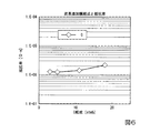
これによって成膜された導電層(窒素、炭素添加クロム膜)は膜厚が約150nmであり、オージェ電子分光法(AES)による密着層の組成分析を表5に示す。また、導電層への炭素添加量と抵抗率との関係のグラフを図6に示す。
"Conductive layer (nitrogen, carbon-added chromium film)"
Sputtering gas: Ar / N 2 / CO 2 (in order of Examples 5 to 8) 47/16/0, 47/16 / 1.5, 45/16/3, 45/16/6 (scom)
CD power: 2.0kW
Target: Cr / φ8 inch The conductive layer (nitrogen, carbon-added chromium film) formed thereby has a thickness of about 150 nm, and Table 5 shows the composition analysis of the adhesion layer by Auger electron spectroscopy (AES). FIG. 6 shows a graph of the relationship between the amount of carbon added to the conductive layer and the resistivity.
次に、成膜された電極膜の上にポジ型感光性レジストを1μmの膜厚となるようにスピンコーターで塗布、露光、現像処理を順次行い、レジストパターンを形成した。そして、レジストパターンをマスクにして硝酸セリウムアンモニウムを主成分とするクロム用エッチング液でクロム膜をエッチングし、レジストを除去して電鋳用マスク原版(電極パターン付きの機能部品)とした。なお成膜された電極膜上にレジスト等の不導体膜を所定膜厚形成した後所望のパターニングを行い、その状態で電鋳用ガラス原版として使用することも可能である。 Next, a positive photosensitive resist was applied on the formed electrode film with a spin coater so as to have a film thickness of 1 μm, exposed, and developed in order to form a resist pattern. Then, using the resist pattern as a mask, the chromium film was etched with a chromium etching solution containing cerium ammonium nitrate as a main component, and the resist was removed to obtain an electroforming mask original plate (functional part with an electrode pattern). It is also possible to form a non-conductive film such as a resist on the formed electrode film and then perform desired patterning and use it as an electroforming glass original plate in that state.
作製した電鋳用マスク原版に対して以下の条件でNi−Fe合金を電鋳(メッキ)し、耐メッキ性の評価をおこなった。メッキ液の組成としては、NiSO4、NiCl2、H3BO3、FeSO4、マロン酸、サッカリン酸を含み、pH2.3程度の酸性度の高いNi−Feメッキ液を用いた。液温は50℃とした。陽極には鉄板および電気ニッケル板を用いた。電源には直流安定化電源を用い,電流密度4A/dm2で定電流電解を行った。膜厚20μmまで電解後,得られた電析膜を十分に水洗し,電鋳用マスク原版(実施例5〜8、密着層(酸化クロム膜)の有無)から機械的に剥離し、電鋳用マスク原版の導電層(および密着層)のダメージを観察し、何回まで電極膜が剥離せずに耐えるかの回数で評価した。(なお、膜厚を20μmに設定した理由は、一般的に電鋳マスクとして想定される膜厚が5〜30μm程度であることによる)。実施例5〜8の耐メッキ性の評価を表6に示す。 A Ni—Fe alloy was electroformed (plated) on the produced electroforming mask original plate under the following conditions, and the plating resistance was evaluated. As the composition of the plating solution, Ni-Fe plating solution containing NiSO 4 , NiCl 2 , H 3 BO 3 , FeSO 4 , malonic acid and saccharic acid and having a high acidity of about pH 2.3 was used. The liquid temperature was 50 ° C. An iron plate and an electric nickel plate were used for the anode. A DC stabilized power source was used as the power source, and constant current electrolysis was performed at a current density of 4 A / dm 2 . After electrolysis to a film thickness of 20 μm, the obtained electrodeposited film is washed thoroughly with water and mechanically peeled off from the electroforming mask master (Examples 5 to 8, presence / absence of adhesion layer (chromium oxide film)). The damage of the conductive layer (and adhesion layer) of the mask original plate was observed and evaluated by the number of times the electrode film could withstand without peeling. (The reason for setting the film thickness to 20 μm is that the film thickness generally assumed as an electroforming mask is about 5 to 30 μm). Table 6 shows the evaluation of the plating resistance of Examples 5 to 8.
表6に示す耐メッキ性の評価によれば、密着層を形成し、また、電極層に窒素および炭素を添加することによって、耐メッキ性が大幅に向上し、複数回の電鋳によるメタルマスクの形成に耐えうる電鋳用マスク原版が得られることが確認された。 According to the evaluation of the plating resistance shown in Table 6, by forming an adhesion layer and adding nitrogen and carbon to the electrode layer, the plating resistance is greatly improved, and a metal mask by multiple times of electroforming. It was confirmed that an electroforming mask original plate that can withstand the formation of is obtained.
1 機能部品(電鋳用マスク原版)
2 電極パターン付きの機能部品
10 ガラス基板
11 密着層
12 導電層
13 電極膜
14 電極パターン
1 Functional parts (mask mask for electroforming)
2 Functional component with
Claims (9)
Priority Applications (1)
| Application Number | Priority Date | Filing Date | Title |
|---|---|---|---|
| JP2016021766A JP6639253B2 (en) | 2016-02-08 | 2016-02-08 | Functional component of mask for electroforming, method of manufacturing functional component of mask for electroforming |
Applications Claiming Priority (1)
| Application Number | Priority Date | Filing Date | Title |
|---|---|---|---|
| JP2016021766A JP6639253B2 (en) | 2016-02-08 | 2016-02-08 | Functional component of mask for electroforming, method of manufacturing functional component of mask for electroforming |
Publications (2)
| Publication Number | Publication Date |
|---|---|
| JP2017141482A true JP2017141482A (en) | 2017-08-17 |
| JP6639253B2 JP6639253B2 (en) | 2020-02-05 |
Family
ID=59627680
Family Applications (1)
| Application Number | Title | Priority Date | Filing Date |
|---|---|---|---|
| JP2016021766A Expired - Fee Related JP6639253B2 (en) | 2016-02-08 | 2016-02-08 | Functional component of mask for electroforming, method of manufacturing functional component of mask for electroforming |
Country Status (1)
| Country | Link |
|---|---|
| JP (1) | JP6639253B2 (en) |
Cited By (1)
| Publication number | Priority date | Publication date | Assignee | Title |
|---|---|---|---|---|
| JP2019157264A (en) * | 2018-03-13 | 2019-09-19 | アドバンテック グローバル リミテッドAdvantech Global Ltd | Iron nickel alloy shadow mask and manufacturing method thereof |
Citations (5)
| Publication number | Priority date | Publication date | Assignee | Title |
|---|---|---|---|---|
| JPS5831336A (en) * | 1981-08-19 | 1983-02-24 | Konishiroku Photo Ind Co Ltd | Raw material of photomask |
| JPH0836171A (en) * | 1994-07-22 | 1996-02-06 | A G Technol Kk | Light-shielding film for liquid crystal display device and liquid crystal display device |
| JP2002055461A (en) * | 2000-05-29 | 2002-02-20 | Tokyo Process Service Kk | Method for producing metallic mask |
| JP2005210093A (en) * | 2003-12-25 | 2005-08-04 | Hoya Corp | Substrate with muti-layer reflective film, exposure reflection type mask blank, exposure reflection type mask, and manufacturing methods for these |
| JP2006215297A (en) * | 2005-02-04 | 2006-08-17 | Shin Etsu Chem Co Ltd | Translucent laminated film, photomask blank, photomask, and manufacturing method thereof |
-
2016
- 2016-02-08 JP JP2016021766A patent/JP6639253B2/en not_active Expired - Fee Related
Patent Citations (5)
| Publication number | Priority date | Publication date | Assignee | Title |
|---|---|---|---|---|
| JPS5831336A (en) * | 1981-08-19 | 1983-02-24 | Konishiroku Photo Ind Co Ltd | Raw material of photomask |
| JPH0836171A (en) * | 1994-07-22 | 1996-02-06 | A G Technol Kk | Light-shielding film for liquid crystal display device and liquid crystal display device |
| JP2002055461A (en) * | 2000-05-29 | 2002-02-20 | Tokyo Process Service Kk | Method for producing metallic mask |
| JP2005210093A (en) * | 2003-12-25 | 2005-08-04 | Hoya Corp | Substrate with muti-layer reflective film, exposure reflection type mask blank, exposure reflection type mask, and manufacturing methods for these |
| JP2006215297A (en) * | 2005-02-04 | 2006-08-17 | Shin Etsu Chem Co Ltd | Translucent laminated film, photomask blank, photomask, and manufacturing method thereof |
Cited By (1)
| Publication number | Priority date | Publication date | Assignee | Title |
|---|---|---|---|---|
| JP2019157264A (en) * | 2018-03-13 | 2019-09-19 | アドバンテック グローバル リミテッドAdvantech Global Ltd | Iron nickel alloy shadow mask and manufacturing method thereof |
Also Published As
| Publication number | Publication date |
|---|---|
| JP6639253B2 (en) | 2020-02-05 |
Similar Documents
| Publication | Publication Date | Title |
|---|---|---|
| US8980076B1 (en) | Electro-deposited passivation coatings for patterned media | |
| CN102317510B (en) | Metal foil, method for producing same, insulating substrate, and wiring board | |
| JPH05504658A (en) | Method for manufacturing printed circuit board patterns using selectively etchable metal layers | |
| JP4959052B2 (en) | Improved method of forming conductive traces and printed circuit manufactured thereby | |
| US20090321267A1 (en) | Method for surface treating plastic products | |
| CN108738249B (en) | Method for manufacturing wiring substrate | |
| TWI593830B (en) | With a carrier of ultra-thin copper foil, copper-clad laminate and coreless substrate | |
| TW201028500A (en) | Method for forming electronic circuit | |
| TWI277377B (en) | Method for manufacturing an electrodeposited copper foil with a high-temperature resistant carrier and an electrodeposited copper foil with a high-temperature resistant carrier obtained through the method | |
| JP6639253B2 (en) | Functional component of mask for electroforming, method of manufacturing functional component of mask for electroforming | |
| TW201101946A (en) | Aluminum substrate circuit board, method of making the same, and electroplating solution for the method | |
| JP3714262B2 (en) | Fine electroforming mold and its manufacturing method | |
| JP5435484B2 (en) | Method for producing metal-filled microstructure | |
| CN204130362U (en) | A kind of plating noble metal switch contact element | |
| JP2007070709A (en) | Electroforming die, method for producing electroforming die, and method for producing electroformed component | |
| JP2006219752A5 (en) | ||
| JP6029202B2 (en) | Method of electroplating pure iron on aluminum or aluminum alloy material | |
| JP2009123980A (en) | Aluminum base heat dissipation board for electric circuit and manufacturing method thereof | |
| WO2022181300A1 (en) | Structure and method for manufacturing structure | |
| JP2011171687A (en) | Insulated substrate, manufacturing method thereof, and forming method of wiring | |
| JP2009052075A (en) | Electrical Fe-Ni alloy plating method and Fe-Ni alloy plating structure | |
| CN114127338B (en) | Method for manufacturing mold for manufacturing fine metal mask and method for manufacturing fine metal mask | |
| JP2000505151A (en) | Method of providing a silver layer on a glass substrate | |
| JPH08335776A (en) | Method for treating copper foil in printed circuit | |
| TW201238752A (en) | Copper foil with copper carrier, method for producing said copper foil, copper foil for electronic circuit, method for producing said copper foil, and method for forming electronic circuit |
Legal Events
| Date | Code | Title | Description |
|---|---|---|---|
| RD03 | Notification of appointment of power of attorney |
Free format text: JAPANESE INTERMEDIATE CODE: A7423 Effective date: 20181116 |
|
| A621 | Written request for application examination |
Free format text: JAPANESE INTERMEDIATE CODE: A621 Effective date: 20181214 |
|
| A131 | Notification of reasons for refusal |
Free format text: JAPANESE INTERMEDIATE CODE: A131 Effective date: 20190910 |
|
| A977 | Report on retrieval |
Free format text: JAPANESE INTERMEDIATE CODE: A971007 Effective date: 20190912 |
|
| A521 | Request for written amendment filed |
Free format text: JAPANESE INTERMEDIATE CODE: A523 Effective date: 20191017 |
|
| TRDD | Decision of grant or rejection written | ||
| A01 | Written decision to grant a patent or to grant a registration (utility model) |
Free format text: JAPANESE INTERMEDIATE CODE: A01 Effective date: 20191126 |
|
| A61 | First payment of annual fees (during grant procedure) |
Free format text: JAPANESE INTERMEDIATE CODE: A61 Effective date: 20191224 |
|
| R150 | Certificate of patent or registration of utility model |
Ref document number: 6639253 Country of ref document: JP Free format text: JAPANESE INTERMEDIATE CODE: R150 |
|
| LAPS | Cancellation because of no payment of annual fees |