JP2017146333A - 表示装置 - Google Patents
表示装置 Download PDFInfo
- Publication number
- JP2017146333A JP2017146333A JP2016025591A JP2016025591A JP2017146333A JP 2017146333 A JP2017146333 A JP 2017146333A JP 2016025591 A JP2016025591 A JP 2016025591A JP 2016025591 A JP2016025591 A JP 2016025591A JP 2017146333 A JP2017146333 A JP 2017146333A
- Authority
- JP
- Japan
- Prior art keywords
- display
- main body
- display surface
- light
- viewed
- Prior art date
- Legal status (The legal status is an assumption and is not a legal conclusion. Google has not performed a legal analysis and makes no representation as to the accuracy of the status listed.)
- Pending
Links
Images







Classifications
-
- G—PHYSICS
- G02—OPTICS
- G02F—OPTICAL DEVICES OR ARRANGEMENTS FOR THE CONTROL OF LIGHT BY MODIFICATION OF THE OPTICAL PROPERTIES OF THE MEDIA OF THE ELEMENTS INVOLVED THEREIN; NON-LINEAR OPTICS; FREQUENCY-CHANGING OF LIGHT; OPTICAL LOGIC ELEMENTS; OPTICAL ANALOGUE/DIGITAL CONVERTERS
- G02F1/00—Devices or arrangements for the control of the intensity, colour, phase, polarisation or direction of light arriving from an independent light source, e.g. switching, gating or modulating; Non-linear optics
- G02F1/01—Devices or arrangements for the control of the intensity, colour, phase, polarisation or direction of light arriving from an independent light source, e.g. switching, gating or modulating; Non-linear optics for the control of the intensity, phase, polarisation or colour
- G02F1/13—Devices or arrangements for the control of the intensity, colour, phase, polarisation or direction of light arriving from an independent light source, e.g. switching, gating or modulating; Non-linear optics for the control of the intensity, phase, polarisation or colour based on liquid crystals, e.g. single liquid crystal display cells
- G02F1/133—Constructional arrangements; Operation of liquid crystal cells; Circuit arrangements
- G02F1/1333—Constructional arrangements; Manufacturing methods
- G02F1/1335—Structural association of cells with optical devices, e.g. polarisers or reflectors
- G02F1/1336—Illuminating devices
- G02F1/133602—Direct backlight
- G02F1/133605—Direct backlight including specially adapted reflectors
-
- H—ELECTRICITY
- H04—ELECTRIC COMMUNICATION TECHNIQUE
- H04N—PICTORIAL COMMUNICATION, e.g. TELEVISION
- H04N5/00—Details of television systems
- H04N5/64—Constructional details of receivers, e.g. cabinets or dust covers
-
- G—PHYSICS
- G02—OPTICS
- G02F—OPTICAL DEVICES OR ARRANGEMENTS FOR THE CONTROL OF LIGHT BY MODIFICATION OF THE OPTICAL PROPERTIES OF THE MEDIA OF THE ELEMENTS INVOLVED THEREIN; NON-LINEAR OPTICS; FREQUENCY-CHANGING OF LIGHT; OPTICAL LOGIC ELEMENTS; OPTICAL ANALOGUE/DIGITAL CONVERTERS
- G02F1/00—Devices or arrangements for the control of the intensity, colour, phase, polarisation or direction of light arriving from an independent light source, e.g. switching, gating or modulating; Non-linear optics
- G02F1/01—Devices or arrangements for the control of the intensity, colour, phase, polarisation or direction of light arriving from an independent light source, e.g. switching, gating or modulating; Non-linear optics for the control of the intensity, phase, polarisation or colour
- G02F1/13—Devices or arrangements for the control of the intensity, colour, phase, polarisation or direction of light arriving from an independent light source, e.g. switching, gating or modulating; Non-linear optics for the control of the intensity, phase, polarisation or colour based on liquid crystals, e.g. single liquid crystal display cells
- G02F1/133—Constructional arrangements; Operation of liquid crystal cells; Circuit arrangements
- G02F1/1333—Constructional arrangements; Manufacturing methods
- G02F1/1335—Structural association of cells with optical devices, e.g. polarisers or reflectors
- G02F1/1336—Illuminating devices
- G02F1/133602—Direct backlight
- G02F1/133608—Direct backlight including particular frames or supporting means
-
- G—PHYSICS
- G02—OPTICS
- G02F—OPTICAL DEVICES OR ARRANGEMENTS FOR THE CONTROL OF LIGHT BY MODIFICATION OF THE OPTICAL PROPERTIES OF THE MEDIA OF THE ELEMENTS INVOLVED THEREIN; NON-LINEAR OPTICS; FREQUENCY-CHANGING OF LIGHT; OPTICAL LOGIC ELEMENTS; OPTICAL ANALOGUE/DIGITAL CONVERTERS
- G02F1/00—Devices or arrangements for the control of the intensity, colour, phase, polarisation or direction of light arriving from an independent light source, e.g. switching, gating or modulating; Non-linear optics
- G02F1/01—Devices or arrangements for the control of the intensity, colour, phase, polarisation or direction of light arriving from an independent light source, e.g. switching, gating or modulating; Non-linear optics for the control of the intensity, phase, polarisation or colour
- G02F1/13—Devices or arrangements for the control of the intensity, colour, phase, polarisation or direction of light arriving from an independent light source, e.g. switching, gating or modulating; Non-linear optics for the control of the intensity, phase, polarisation or colour based on liquid crystals, e.g. single liquid crystal display cells
- G02F1/133—Constructional arrangements; Operation of liquid crystal cells; Circuit arrangements
- G02F1/1333—Constructional arrangements; Manufacturing methods
- G02F1/133308—Support structures for LCD panels, e.g. frames or bezels
-
- G—PHYSICS
- G02—OPTICS
- G02F—OPTICAL DEVICES OR ARRANGEMENTS FOR THE CONTROL OF LIGHT BY MODIFICATION OF THE OPTICAL PROPERTIES OF THE MEDIA OF THE ELEMENTS INVOLVED THEREIN; NON-LINEAR OPTICS; FREQUENCY-CHANGING OF LIGHT; OPTICAL LOGIC ELEMENTS; OPTICAL ANALOGUE/DIGITAL CONVERTERS
- G02F1/00—Devices or arrangements for the control of the intensity, colour, phase, polarisation or direction of light arriving from an independent light source, e.g. switching, gating or modulating; Non-linear optics
- G02F1/01—Devices or arrangements for the control of the intensity, colour, phase, polarisation or direction of light arriving from an independent light source, e.g. switching, gating or modulating; Non-linear optics for the control of the intensity, phase, polarisation or colour
- G02F1/13—Devices or arrangements for the control of the intensity, colour, phase, polarisation or direction of light arriving from an independent light source, e.g. switching, gating or modulating; Non-linear optics for the control of the intensity, phase, polarisation or colour based on liquid crystals, e.g. single liquid crystal display cells
- G02F1/133—Constructional arrangements; Operation of liquid crystal cells; Circuit arrangements
- G02F1/1333—Constructional arrangements; Manufacturing methods
- G02F1/133308—Support structures for LCD panels, e.g. frames or bezels
- G02F1/133314—Back frames
-
- G—PHYSICS
- G02—OPTICS
- G02F—OPTICAL DEVICES OR ARRANGEMENTS FOR THE CONTROL OF LIGHT BY MODIFICATION OF THE OPTICAL PROPERTIES OF THE MEDIA OF THE ELEMENTS INVOLVED THEREIN; NON-LINEAR OPTICS; FREQUENCY-CHANGING OF LIGHT; OPTICAL LOGIC ELEMENTS; OPTICAL ANALOGUE/DIGITAL CONVERTERS
- G02F1/00—Devices or arrangements for the control of the intensity, colour, phase, polarisation or direction of light arriving from an independent light source, e.g. switching, gating or modulating; Non-linear optics
- G02F1/01—Devices or arrangements for the control of the intensity, colour, phase, polarisation or direction of light arriving from an independent light source, e.g. switching, gating or modulating; Non-linear optics for the control of the intensity, phase, polarisation or colour
- G02F1/13—Devices or arrangements for the control of the intensity, colour, phase, polarisation or direction of light arriving from an independent light source, e.g. switching, gating or modulating; Non-linear optics for the control of the intensity, phase, polarisation or colour based on liquid crystals, e.g. single liquid crystal display cells
- G02F1/133—Constructional arrangements; Operation of liquid crystal cells; Circuit arrangements
- G02F1/1333—Constructional arrangements; Manufacturing methods
- G02F1/1335—Structural association of cells with optical devices, e.g. polarisers or reflectors
- G02F1/1336—Illuminating devices
- G02F1/133602—Direct backlight
- G02F1/133603—Direct backlight with LEDs
-
- G—PHYSICS
- G02—OPTICS
- G02F—OPTICAL DEVICES OR ARRANGEMENTS FOR THE CONTROL OF LIGHT BY MODIFICATION OF THE OPTICAL PROPERTIES OF THE MEDIA OF THE ELEMENTS INVOLVED THEREIN; NON-LINEAR OPTICS; FREQUENCY-CHANGING OF LIGHT; OPTICAL LOGIC ELEMENTS; OPTICAL ANALOGUE/DIGITAL CONVERTERS
- G02F2201/00—Constructional arrangements not provided for in groups G02F1/00 - G02F7/00
- G02F2201/46—Fixing elements
- G02F2201/465—Snap -fit
Landscapes
- Physics & Mathematics (AREA)
- Nonlinear Science (AREA)
- Optics & Photonics (AREA)
- Crystallography & Structural Chemistry (AREA)
- Chemical & Material Sciences (AREA)
- General Physics & Mathematics (AREA)
- Mathematical Physics (AREA)
- Liquid Crystal (AREA)
- Engineering & Computer Science (AREA)
- Multimedia (AREA)
- Signal Processing (AREA)
- Devices For Indicating Variable Information By Combining Individual Elements (AREA)
- Planar Illumination Modules (AREA)
Abstract
Description
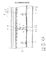
図1〜図7を参照して、本発明の第1実施形態による液晶テレビジョン装置100の構成について説明する。なお、液晶テレビジョン装置100は、特許請求の範囲の「表示装置」の一例である。
本発明の第1実施形態による液晶テレビジョン装置100は、図1に示すように、表示部1と、前部筐体2と、リアフレーム3と、液晶テレビジョン装置100全体を支持するスタンド部4とを備えている。なお、リアフレーム3は、特許請求の範囲の「筐体」の一例である。
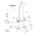
パネルポスト9は、図3に示すように、光源部6と離間して配置されている。また、パネルポスト9は、透光性を有する樹脂材料により形成されている。具体的には、パネルポスト9は、支持部9aと、突出部9bと、フック形状部9cと、凸形状部9dとを含んでいる。なお、支持部9aは、特許請求の範囲の「本体部」の一例である。
次に、図7を参照して、パネルポスト9の内側に侵入した光の経路について説明する。
第1実施形態では、以下のような効果を得ることができる。
次に、図1および図8を参照して、第2実施形態について説明する。この第2実施形態では、反射シート7に対して平行に配置されたリアフレーム3の孔部(第1孔部3bおよび第2孔部3c)に、パネルポスト9を係合させた上記第1実施形態と異なり、反射シート7を貫通したリアフレーム203の切り起こし部203fに、パネルポスト209を係合させる例について説明する。なお、上記第1実施形態と同様の構成は、第1実施形態と同じ符号を付して図示するとともに説明を省略する。なお、リアフレーム203は、特許請求の範囲の「筐体」の一例である。また、パネルポスト209は、特許請求の範囲の「柱部」の一例である。
図8に示すように、第2実施形態による液晶テレビジョン装置200(図1参照)では、リアフレーム203には、反射シート7を前方(Y1方向)に貫通して表示部1側に突出する一対の切り起こし部203fが形成されている。また、パネルポスト209には、光学シート8と平行な方向(X1方向およびX2方向)に突出する一対の係合突起部209fが形成されている。なお、液晶テレビジョン装置200は、特許請求の範囲の「表示装置」の一例である。また、切り起こし部203fは、特許請求の範囲の「第1係合部」の一例である。また、係合突起部209fは、特許請求の範囲の「第2係合部」の一例である。
第2実施形態では、以下のような効果を得ることができる。
次に、図1および図9を参照して、第3実施形態について説明する。この第3実施形態では、パネルポスト9の支持部9aの後方(Y2方向)に、反射シート7を配置した上記第1実施形態と異なり、パネルポスト9の支持部9aの後方(Y2方向)に、反射シート7ではなく、パネルポスト用反射シート307を配置する例について説明する。なお、上記第1実施形態と同様の構成は、第1実施形態と同じ符号を付して図示するとともに説明を省略する。また、パネルポスト用反射シート307は、特許請求の範囲の「第2反射部」の一例である。
図9に示すように、第3実施形態による液晶テレビジョン装置300(図1参照)は、表示面1aに直交する方向(Y方向)から見て、支持部9aの全域と重なるように配置されるパネルポスト用反射シート307を含んでいる。このパネルポスト用反射シート307は、リアフレーム3と、支持部9a(突出部9b)との間に配置されている。また、パネルポスト用反射シート307は、反射シート7よりも高い光の反射率を有している。なお、液晶テレビジョン装置300は、特許請求の範囲の「表示装置」の一例である。
第3実施形態では、以下のような効果を得ることができる。
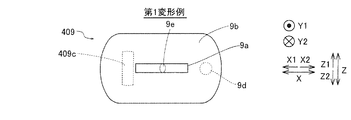
なお、今回開示された実施形態は、すべての点で例示であって制限的なものではないと考えられるべきである。本発明の範囲は、上記した実施形態の説明ではなく特許請求の範囲によって示され、さらに特許請求の範囲と均等の意味および範囲内でのすべての変更(変形例)が含まれる。
1a 表示面
3、203、603 リアフレーム(筺体)
3b 第1孔部(第1係合部)
3c 第2孔部(第1係合部)
6 光源部
7 反射シート(第1反射部、反射部)
8 光学シート(光学部)
9、209、409、509、609、709、809 パネルポスト(柱部)
9a、709a 支持部(本体部)
9b、709b 突出部
9c、409c、509c フック形状部(第2係合部)
9d、509d 凸形状部(第2係合部)
90a、90b、290 接続部分
100、200、300 液晶テレビジョン装置(表示装置)
203f 切り起こし部(第1係合部)
209f 係合突起部(第2係合部)
307 パネルポスト用反射シート(第2反射部、反射部)
603c 孔部(第1係合部)
609f、809f フック部(第2係合部)
Claims (7)
- 表示部と、
第1係合部を含み、前記表示部の表示面と異なる面側に配置される筐体と、
光源部と、
前記表示部と前記光源部との間に配置され、前記光源部からの光を受けて表示部側に出射する光学部と、
前記筐体から前記光学部側に突出する透光性を有する本体部を含む柱部を備え、
前記柱部は、前記本体部から前記表示部の表示面と平行な方向に突出する突出部と、前記突出部に設けられ、前記第1係合部に係合する第2係合部とを含み、
前記第2係合部と前記突出部との接続部分は、前記表示面に直交する方向から見て、前記本体部と略重ならないように配置されている、表示装置。 - 前記筐体と前記本体部との間に配置されるとともに、前記表示面に直交する方向から見て、前記本体部と前記光学部とが接触する領域の略全域と重なるように配置され、前記光源部からの光を反射可能に構成された反射部をさらに備える、請求項1に記載の表示装置。
- 前記反射部は、前記表示面に直交する方向から見て、前記本体部全域に対して、前記本体部と重なる領域の占める割合が80%以上となるように配置されている、請求項2に記載の表示装置。
- 前記反射部は、前記表示面に直交する方向から見て、前記本体部の略全域と重なるように配置されている、請求項3に記載の表示装置。
- 前記第2係合部は、複数設けられており、
複数の前記第2係合部は、少なくとも、前記本体部を挟むように前記本体部の両側に設けられている、請求項1〜4のいずれか1項に記載の表示装置。 - 前記第1係合部は、前記反射部を貫通して前記表示部側に突出するように形成され、
前記第2係合部は、前記表示部の表示面と平行な方向に突出するように形成されている、請求項1〜5のいずれか1項に記載の表示装置。 - 前記反射部は、前記筐体の前記表示部側の面に沿って配置される第1反射部と、
前記筐体と前記本体部との間に配置されるとともに、前記表示面に直交する方向から見て、前記本体部と重なるように配置される第2反射部とを含み、
前記第2反射部は、前記第1反射部よりも高い光の反射率を有している、請求項2〜4のいずれか1項に記載の表示装置。
Priority Applications (7)
| Application Number | Priority Date | Filing Date | Title |
|---|---|---|---|
| JP2016025591A JP2017146333A (ja) | 2016-02-15 | 2016-02-15 | 表示装置 |
| US15/430,635 US10353241B2 (en) | 2016-02-15 | 2017-02-13 | Display device |
| EP17156071.7A EP3206080B1 (en) | 2016-02-15 | 2017-02-14 | Display device |
| EP19150265.7A EP3492970B1 (en) | 2016-02-15 | 2017-02-14 | Display device |
| CN201811622263.0A CN109917586B (zh) | 2016-02-15 | 2017-02-15 | 显示装置 |
| CN201710081519.0A CN107087128B (zh) | 2016-02-15 | 2017-02-15 | 显示装置 |
| US16/240,052 US10725338B2 (en) | 2016-02-15 | 2019-01-04 | Display device |
Applications Claiming Priority (1)
| Application Number | Priority Date | Filing Date | Title |
|---|---|---|---|
| JP2016025591A JP2017146333A (ja) | 2016-02-15 | 2016-02-15 | 表示装置 |
Publications (1)
| Publication Number | Publication Date |
|---|---|
| JP2017146333A true JP2017146333A (ja) | 2017-08-24 |
Family
ID=58046537
Family Applications (1)
| Application Number | Title | Priority Date | Filing Date |
|---|---|---|---|
| JP2016025591A Pending JP2017146333A (ja) | 2016-02-15 | 2016-02-15 | 表示装置 |
Country Status (4)
| Country | Link |
|---|---|
| US (2) | US10353241B2 (ja) |
| EP (2) | EP3206080B1 (ja) |
| JP (1) | JP2017146333A (ja) |
| CN (2) | CN109917586B (ja) |
Cited By (2)
| Publication number | Priority date | Publication date | Assignee | Title |
|---|---|---|---|---|
| JP2019091036A (ja) * | 2017-11-13 | 2019-06-13 | エルジー ディスプレイ カンパニー リミテッド | 異形液晶発光装置 |
| WO2023101055A1 (ko) * | 2021-12-02 | 2023-06-08 | 엘지전자 주식회사 | 디스플레이 디바이스 |
Families Citing this family (5)
| Publication number | Priority date | Publication date | Assignee | Title |
|---|---|---|---|---|
| CN107765471A (zh) * | 2017-09-08 | 2018-03-06 | 伟志光电(深圳)有限公司 | 一种铝铸件凹形曲面结构的背光源 |
| TWI669545B (zh) * | 2018-02-23 | 2019-08-21 | 友達光電股份有限公司 | 顯示裝置及其背光模組 |
| JP2021131502A (ja) * | 2020-02-21 | 2021-09-09 | 船井電機株式会社 | 表示装置 |
| KR102513631B1 (ko) * | 2022-11-23 | 2023-03-24 | 주식회사 케이홀로 | 배경의 입체효과와 음영을 이용한 투명 디스플레이 기반의 영상 재생 장치 |
| TWI840119B (zh) * | 2023-02-10 | 2024-04-21 | 瑞軒科技股份有限公司 | 顯示器及其背光模組、支撐柱 |
Family Cites Families (36)
| Publication number | Priority date | Publication date | Assignee | Title |
|---|---|---|---|---|
| US6974221B2 (en) * | 2003-12-30 | 2005-12-13 | Au Optronics Corporation | Support for backlight module |
| JP4491634B2 (ja) * | 2004-01-23 | 2010-06-30 | 日本電気株式会社 | 直下型バックライト及び表示装置 |
| JP4265470B2 (ja) | 2004-04-16 | 2009-05-20 | 日立電線株式会社 | 波長多重光伝送モジュール及びその調芯方法 |
| TWI283321B (en) * | 2004-06-18 | 2007-07-01 | Au Optronics Corp | Supporter and LED light-source module using the same |
| JP4072519B2 (ja) * | 2004-06-18 | 2008-04-09 | シャープ株式会社 | 表示装置用照明装置 |
| JP4543813B2 (ja) * | 2004-08-04 | 2010-09-15 | ソニー株式会社 | バックライト装置及びこのバックライト装置を備えた液晶表示装置 |
| WO2006059411A1 (ja) * | 2004-11-30 | 2006-06-08 | Sharp Kabushiki Kaisha | 表示装置用照明装置、および表示装置 |
| TWI255896B (en) * | 2005-01-19 | 2006-06-01 | Au Optronics Corp | Backlight module |
| KR101129427B1 (ko) * | 2005-03-09 | 2012-06-12 | 삼성전자주식회사 | 백라이트 어셈블리 및 이를 갖는 표시장치 |
| JP4648070B2 (ja) | 2005-04-27 | 2011-03-09 | 株式会社 日立ディスプレイズ | 表示装置 |
| US7739088B2 (en) * | 2005-07-07 | 2010-06-15 | Fuji Jukogyo Kabushiki Kaisha | Method and program for simulating occurrence of air pocket |
| KR20070015657A (ko) * | 2005-08-01 | 2007-02-06 | 삼성전자주식회사 | 백라이트 유닛 및 이를 포함하는 액정표시장치 |
| KR20070016206A (ko) * | 2005-08-02 | 2007-02-07 | 삼성전자주식회사 | 액정표시장치 |
| JP4896669B2 (ja) | 2005-11-02 | 2012-03-14 | 三星電子株式会社 | バックライトアセンブリ、これを有する液晶表示装置、及びランプ固定部材の製造方法 |
| US8104911B2 (en) * | 2007-09-28 | 2012-01-31 | Apple Inc. | Display system with distributed LED backlight |
| EP2192341A4 (en) * | 2007-10-24 | 2013-03-13 | Sharp Kk | LIGHTING DEVICE FOR A DISPLAY DEVICE, DISPLAY DEVICE AND TV RECEIVER |
| JP4968014B2 (ja) * | 2007-11-22 | 2012-07-04 | ソニー株式会社 | バックライト装置及び液晶表示装置 |
| US20090284444A1 (en) * | 2008-05-16 | 2009-11-19 | Jeffrey Allen Wilson | Removable optical filter and retainer |
| JP4631938B2 (ja) * | 2008-06-18 | 2011-02-16 | ソニー株式会社 | クリップ及びバックライトアッセンブリ |
| TWI369549B (en) * | 2008-09-26 | 2012-08-01 | Au Optronics Corp | Backlight module |
| RU2473836C1 (ru) * | 2008-11-28 | 2013-01-27 | Шарп Кабусики Кайся | Устройство освещения, устройство отображения и телевизионный приемник |
| CN102265086A (zh) * | 2008-12-25 | 2011-11-30 | 夏普株式会社 | 框架、光源装置、显示装置和电视接收机 |
| JP4621799B1 (ja) * | 2009-05-22 | 2011-01-26 | シャープ株式会社 | 光反射シート、光源装置及び表示装置 |
| US8547499B2 (en) | 2009-06-15 | 2013-10-01 | Sharp Kabushiki Kaisha | Lighting device, display device and television receiver |
| JP5228108B2 (ja) * | 2009-07-21 | 2013-07-03 | シャープ株式会社 | 支持ピン、照明装置、表示装置、およびテレビ受像装置 |
| JP5286417B2 (ja) | 2009-09-16 | 2013-09-11 | シャープ株式会社 | 照明装置、表示装置、及びテレビ受信装置 |
| WO2011033900A1 (ja) * | 2009-09-16 | 2011-03-24 | シャープ株式会社 | 照明装置、表示装置、及びテレビ受信装置 |
| US9124898B2 (en) * | 2010-07-12 | 2015-09-01 | Mediatek Inc. | Method and apparatus of temporal motion vector prediction |
| TWI457660B (zh) * | 2011-08-15 | 2014-10-21 | Au Optronics Corp | 可減少漏光之背光模組及顯示裝置 |
| TWI589962B (zh) * | 2011-11-04 | 2017-07-01 | 奇菱光電股份有限公司 | 直下式背光模組 |
| US9128326B2 (en) | 2012-02-07 | 2015-09-08 | Samsung Electronics Co., Ltd. | Supporting member for backlight unit, backlight unit and image display apparatus having the same |
| KR101544608B1 (ko) | 2012-05-25 | 2015-08-17 | 삼성디스플레이 주식회사 | 표시장치 |
| JP2014013690A (ja) * | 2012-07-04 | 2014-01-23 | Sony Corp | 表示装置 |
| CN106233195A (zh) * | 2014-07-07 | 2016-12-14 | 堺显示器制品株式会社 | 光源装置和显示装置 |
| JP2016029470A (ja) * | 2014-07-24 | 2016-03-03 | 船井電機株式会社 | 表示装置 |
| CN104965351A (zh) * | 2015-07-27 | 2015-10-07 | 苏州固特斯电子科技有限公司 | 一种液晶显示模组 |
-
2016
- 2016-02-15 JP JP2016025591A patent/JP2017146333A/ja active Pending
-
2017
- 2017-02-13 US US15/430,635 patent/US10353241B2/en active Active
- 2017-02-14 EP EP17156071.7A patent/EP3206080B1/en active Active
- 2017-02-14 EP EP19150265.7A patent/EP3492970B1/en not_active Not-in-force
- 2017-02-15 CN CN201811622263.0A patent/CN109917586B/zh not_active Expired - Fee Related
- 2017-02-15 CN CN201710081519.0A patent/CN107087128B/zh not_active Expired - Fee Related
-
2019
- 2019-01-04 US US16/240,052 patent/US10725338B2/en active Active
Cited By (4)
| Publication number | Priority date | Publication date | Assignee | Title |
|---|---|---|---|---|
| JP2019091036A (ja) * | 2017-11-13 | 2019-06-13 | エルジー ディスプレイ カンパニー リミテッド | 異形液晶発光装置 |
| US10698259B2 (en) | 2017-11-13 | 2020-06-30 | Lg Display Co., Ltd. | Deformed liquid crystal display device |
| WO2023101055A1 (ko) * | 2021-12-02 | 2023-06-08 | 엘지전자 주식회사 | 디스플레이 디바이스 |
| US12455475B2 (en) | 2021-12-02 | 2025-10-28 | Lg Electronics Inc. | Display device |
Also Published As
| Publication number | Publication date |
|---|---|
| CN109917586A (zh) | 2019-06-21 |
| EP3206080B1 (en) | 2021-05-05 |
| EP3206080A1 (en) | 2017-08-16 |
| US10725338B2 (en) | 2020-07-28 |
| CN109917586B (zh) | 2021-09-03 |
| CN107087128B (zh) | 2020-03-31 |
| US10353241B2 (en) | 2019-07-16 |
| EP3492970B1 (en) | 2020-07-22 |
| US20190137823A1 (en) | 2019-05-09 |
| EP3492970A1 (en) | 2019-06-05 |
| CN107087128A (zh) | 2017-08-22 |
| US20170235189A1 (en) | 2017-08-17 |
Similar Documents
| Publication | Publication Date | Title |
|---|---|---|
| CN100474073C (zh) | 显示装置 | |
| US10598847B2 (en) | Light source module and prism sheet thereof | |
| US10725338B2 (en) | Display device | |
| JP2014085676A (ja) | 曲面ディスプレイ装置 | |
| CN103807669A (zh) | 面光源装置 | |
| JP4458125B2 (ja) | インジケータ装置およびテレビジョン装置 | |
| JP2013187059A (ja) | 導光板及び面光源装置 | |
| JP2015203724A (ja) | 表示装置 | |
| JP6277630B2 (ja) | 表示装置 | |
| US8681293B2 (en) | Liquid crystal display device | |
| JP2004265813A (ja) | 面光源装置および表示装置 | |
| JP2017083692A (ja) | 拡散レンズおよび表示装置 | |
| JP4708440B2 (ja) | 面光源装置 | |
| JP6146032B2 (ja) | 表示装置 | |
| JP2012079681A (ja) | 導光板及び面光源装置 | |
| JP5375845B2 (ja) | 面光源装置および液晶表示装置 | |
| WO2014038312A1 (ja) | 光源モジュール、照明モジュール及び照明機器 | |
| US20150369987A1 (en) | Backlight assembly and display device having the same | |
| JP2008251373A (ja) | 面発光装置 | |
| KR102840171B1 (ko) | 디스플레이 장치 | |
| JP5078640B2 (ja) | 照明装置及びこれを用いた液晶表示装置 | |
| JP2007294372A (ja) | 面光源装置及び表示装置 | |
| JP6711736B2 (ja) | 面状照明装置 | |
| JP2021174711A (ja) | 画像表示装置 | |
| KR20120085181A (ko) | 도광판 및 면광원 장치 |
Legal Events
| Date | Code | Title | Description |
|---|---|---|---|
| A621 | Written request for application examination |
Free format text: JAPANESE INTERMEDIATE CODE: A621 Effective date: 20181218 |
|
| A131 | Notification of reasons for refusal |
Free format text: JAPANESE INTERMEDIATE CODE: A131 Effective date: 20191008 |
|
| A977 | Report on retrieval |
Free format text: JAPANESE INTERMEDIATE CODE: A971007 Effective date: 20191009 |
|
| A521 | Request for written amendment filed |
Free format text: JAPANESE INTERMEDIATE CODE: A523 Effective date: 20191127 |
|
| A131 | Notification of reasons for refusal |
Free format text: JAPANESE INTERMEDIATE CODE: A131 Effective date: 20191217 |
|
| A521 | Request for written amendment filed |
Free format text: JAPANESE INTERMEDIATE CODE: A523 Effective date: 20200205 |
|
| A02 | Decision of refusal |
Free format text: JAPANESE INTERMEDIATE CODE: A02 Effective date: 20200512 |