JP2017147639A - Signal reproduction circuit, electronic device, and signal reproduction method - Google Patents
Signal reproduction circuit, electronic device, and signal reproduction method Download PDFInfo
- Publication number
- JP2017147639A JP2017147639A JP2016028838A JP2016028838A JP2017147639A JP 2017147639 A JP2017147639 A JP 2017147639A JP 2016028838 A JP2016028838 A JP 2016028838A JP 2016028838 A JP2016028838 A JP 2016028838A JP 2017147639 A JP2017147639 A JP 2017147639A
- Authority
- JP
- Japan
- Prior art keywords
- clock
- phase
- frequency
- signal
- circuit
- Prior art date
- Legal status (The legal status is an assumption and is not a legal conclusion. Google has not performed a legal analysis and makes no representation as to the accuracy of the status listed.)
- Granted
Links
Images







Classifications
-
- H—ELECTRICITY
- H04—ELECTRIC COMMUNICATION TECHNIQUE
- H04L—TRANSMISSION OF DIGITAL INFORMATION, e.g. TELEGRAPHIC COMMUNICATION
- H04L7/00—Arrangements for synchronising receiver with transmitter
- H04L7/02—Speed or phase control by the received code signals, the signals containing no special synchronisation information
- H04L7/033—Speed or phase control by the received code signals, the signals containing no special synchronisation information using the transitions of the received signal to control the phase of the synchronising-signal-generating means, e.g. using a phase-locked loop
- H04L7/0331—Speed or phase control by the received code signals, the signals containing no special synchronisation information using the transitions of the received signal to control the phase of the synchronising-signal-generating means, e.g. using a phase-locked loop with a digital phase-locked loop [PLL] processing binary samples, e.g. add/subtract logic for correction of receiver clock
-
- H—ELECTRICITY
- H03—ELECTRONIC CIRCUITRY
- H03L—AUTOMATIC CONTROL, STARTING, SYNCHRONISATION OR STABILISATION OF GENERATORS OF ELECTRONIC OSCILLATIONS OR PULSES
- H03L7/00—Automatic control of frequency or phase; Synchronisation
- H03L7/06—Automatic control of frequency or phase; Synchronisation using a reference signal applied to a frequency- or phase-locked loop
- H03L7/08—Details of the phase-locked loop
- H03L7/0805—Details of the phase-locked loop the loop being adapted to provide an additional control signal for use outside the loop
-
- H—ELECTRICITY
- H03—ELECTRONIC CIRCUITRY
- H03L—AUTOMATIC CONTROL, STARTING, SYNCHRONISATION OR STABILISATION OF GENERATORS OF ELECTRONIC OSCILLATIONS OR PULSES
- H03L7/00—Automatic control of frequency or phase; Synchronisation
- H03L7/06—Automatic control of frequency or phase; Synchronisation using a reference signal applied to a frequency- or phase-locked loop
- H03L7/08—Details of the phase-locked loop
- H03L7/0807—Details of the phase-locked loop concerning mainly a recovery circuit for the reference signal
-
- H—ELECTRICITY
- H03—ELECTRONIC CIRCUITRY
- H03L—AUTOMATIC CONTROL, STARTING, SYNCHRONISATION OR STABILISATION OF GENERATORS OF ELECTRONIC OSCILLATIONS OR PULSES
- H03L7/00—Automatic control of frequency or phase; Synchronisation
- H03L7/06—Automatic control of frequency or phase; Synchronisation using a reference signal applied to a frequency- or phase-locked loop
- H03L7/08—Details of the phase-locked loop
- H03L7/085—Details of the phase-locked loop concerning mainly the frequency- or phase-detection arrangement including the filtering or amplification of its output signal
- H03L7/087—Details of the phase-locked loop concerning mainly the frequency- or phase-detection arrangement including the filtering or amplification of its output signal using at least two phase detectors or a frequency and phase detector in the loop
-
- H—ELECTRICITY
- H03—ELECTRONIC CIRCUITRY
- H03L—AUTOMATIC CONTROL, STARTING, SYNCHRONISATION OR STABILISATION OF GENERATORS OF ELECTRONIC OSCILLATIONS OR PULSES
- H03L7/00—Automatic control of frequency or phase; Synchronisation
- H03L7/06—Automatic control of frequency or phase; Synchronisation using a reference signal applied to a frequency- or phase-locked loop
- H03L7/08—Details of the phase-locked loop
- H03L7/099—Details of the phase-locked loop concerning mainly the controlled oscillator of the loop
-
- H—ELECTRICITY
- H04—ELECTRIC COMMUNICATION TECHNIQUE
- H04L—TRANSMISSION OF DIGITAL INFORMATION, e.g. TELEGRAPHIC COMMUNICATION
- H04L7/00—Arrangements for synchronising receiver with transmitter
- H04L7/0004—Initialisation of the receiver
-
- H—ELECTRICITY
- H04—ELECTRIC COMMUNICATION TECHNIQUE
- H04L—TRANSMISSION OF DIGITAL INFORMATION, e.g. TELEGRAPHIC COMMUNICATION
- H04L7/00—Arrangements for synchronising receiver with transmitter
- H04L7/02—Speed or phase control by the received code signals, the signals containing no special synchronisation information
- H04L7/033—Speed or phase control by the received code signals, the signals containing no special synchronisation information using the transitions of the received signal to control the phase of the synchronising-signal-generating means, e.g. using a phase-locked loop
Landscapes
- Engineering & Computer Science (AREA)
- Computer Networks & Wireless Communication (AREA)
- Signal Processing (AREA)
- Stabilization Of Oscillater, Synchronisation, Frequency Synthesizers (AREA)
Abstract
【課題】ロック状態から非ロック状態に変化したことを、周波数位相検出回路によらず検出する信号再生回路の実現。【解決手段】周波数が可変の第1クロックCLK-Iを発生する発振器41と、入力データDataとCLK-Iの位相関係に応じて、DataとCLK-Iが同期するように発振器を制御するフィードバック回路と、を有し、フィードバック回路は、発振器の制御部と、DataとCLK-Iの位相関係に応じてクロック位相制御信号PDIを生成する第1位相検出回路42と、クロック位相制御信号の高周波成分または低周波数成分の振幅の大きさからロック状態であるか非ロック状態であるかを検出する状態検出回路51-53と、を有する信号再生回路。【選択図】図5A signal reproduction circuit for detecting a change from a locked state to an unlocked state without using a frequency phase detection circuit. An oscillator 41 for generating a first clock CLK-I having a variable frequency, and feedback for controlling the oscillator so that Data and CLK-I are synchronized according to a phase relationship between input data Data and CLK-I. A feedback circuit, a control unit of the oscillator, a first phase detection circuit 42 that generates a clock phase control signal PDI according to the phase relationship between Data and CLK-I, and a high frequency of the clock phase control signal And a state detection circuit 51-53 for detecting whether the component is in the locked state or in the unlocked state based on the magnitude of the amplitude of the component or the low frequency component. [Selection] Figure 5
Description
本発明は、信号再生(クロック・データ・リカバリィ(Clock Data Recovery: CDR))回路、信号再生回路を搭載した電子装置、および信号再生方法に関する。 The present invention relates to a signal recovery (Clock Data Recovery (CDR)) circuit, an electronic device equipped with the signal recovery circuit, and a signal recovery method.
通信基幹向け装置やサーバ等の情報処理機器の性能向上に伴い、装置内外での信号送受信のデータレートを高くすることが要望されている。例えば、集積回路チップ内、チップ間(装置内、装置間)で信号を送受信する高速I/Oの分野、光通信の分野で、ビットレートの一層の高速化が望まれている。 As the performance of information processing equipment such as a communication backbone device and a server is improved, it is desired to increase the data rate of signal transmission and reception inside and outside the device. For example, higher bit rates are desired in the field of high-speed I / O for transmitting and receiving signals between integrated circuit chips and between chips (inside and between devices) and in the field of optical communications.
受信回路では、伝送されてきたデータを適切なタイミングで判定し、データとクロックを再生(CDR: Clock and Data Recovery)することが求められる。入力データと受信(サンプリング)クロックとの位相差および周波数差を検出し、その情報を基にサンプリングクロックの位相調整を行うことによってCDRが実現される。受信回路の中でもリファレンスクロックを用いず、入力データから再生したクロックによってリタイムし、ジッタを削減したデータを出力するCDR回路が知られている。 The receiving circuit is required to determine the transmitted data at an appropriate timing and reproduce the data and clock (CDR: Clock and Data Recovery). The CDR is realized by detecting the phase difference and frequency difference between the input data and the reception (sampling) clock and adjusting the phase of the sampling clock based on the information. Among the receiving circuits, there is known a CDR circuit that does not use a reference clock but outputs data that is retimed by a clock regenerated from input data and reduces jitter.
CDR回路では、入力データとクロックとの位相差を検出する位相検出回路(Phase Detector: PD)を利用することが知られている。位相検出回路の検出した位相差に基づいて、入力データと第1クロックの位相および周波数が一致するように制御される。周波数が一致した状態をロック状態と称する。なお、ロック状態でない状態をここでは非ロック状態と称する。 It is known that a CDR circuit uses a phase detector (PD) that detects a phase difference between input data and a clock. Based on the phase difference detected by the phase detection circuit, control is performed so that the phase and frequency of the input data and the first clock coincide. A state in which the frequencies coincide with each other is referred to as a lock state. Here, a state that is not in the locked state is referred to as a non-locked state here.
しかし、位相検出回路は、クロック再生が可能な周波数範囲が狭く、ロック状態から非ロック状態に変化したことが検出できないという問題がある。 However, the phase detection circuit has a problem that the frequency range in which the clock can be reproduced is narrow, and it cannot be detected that the lock state has changed to the non-lock state.
実施形態によれば、ロック状態から非ロック状態に変化したことを、位相検出回路の出力から検出する信号再生回路が実現される。 According to the embodiment, a signal regeneration circuit that detects from the output of the phase detection circuit that the state has changed from the locked state to the unlocked state is realized.
第1の態様の信号再生回路は、周波数が可変の第1クロックを発生する発振器と、入力データと第1クロックの位相関係に応じて、入力データと第1クロックが同期するように発振器を制御するフィードバック回路と、を有する。フィードバック回路は、入力データと第1クロックの位相関係に応じて発振器を制御する制御部と、入力データと第1クロックの位相関係に応じてクロック位相制御信号を生成する第1位相検出回路と、状態検出回路と、を有する。状態検出回路は、クロック位相制御信号の高周波成分または低周波数成分の振幅の大きさからロック状態であるか非ロック状態であるかを検出する。 The signal reproduction circuit according to the first aspect controls an oscillator so that the input data and the first clock are synchronized according to the phase relationship between the input data and the first clock, and the oscillator that generates the first clock having a variable frequency. A feedback circuit. The feedback circuit includes a control unit that controls the oscillator according to the phase relationship between the input data and the first clock, a first phase detection circuit that generates a clock phase control signal according to the phase relationship between the input data and the first clock, A state detection circuit. The state detection circuit detects whether the state is the locked state or the unlocked state from the magnitude of the amplitude of the high-frequency component or low-frequency component of the clock phase control signal.
第2の態様の信号再生方法は、受信した入力データからクロックを再生する信号再生方法であって、周波数が可変の第1クロックを発生する。さらに、入力データと第1クロックの位相関係に応じてクロック位相制御信号を生成し、クロック位相制御信号の高周波成分または低周波数成分の振幅の大きさからロック状態であるか非ロック状態であるかを検出する。そして、クロック位相制御信号に応じて、入力データと第1クロックが同期するように第1クロックの周波数を制御するフィードバック制御を行う。 The signal reproduction method according to the second aspect is a signal reproduction method for reproducing a clock from received input data, and generates a first clock having a variable frequency. Furthermore, a clock phase control signal is generated according to the phase relationship between the input data and the first clock, and whether the clock phase control signal is in a locked state or an unlocked state based on the magnitude of the amplitude of the high frequency component or low frequency component Is detected. Then, feedback control is performed to control the frequency of the first clock so that the input data and the first clock are synchronized in accordance with the clock phase control signal.
実施形態の信号再生回路は、位相検出回路の出力からロック状態から非ロック状態に変化したことを検出可能である。 The signal reproduction circuit of the embodiment can detect that the output from the phase detection circuit has changed from the locked state to the unlocked state.
実施形態を説明する前に、一般的なクロック・データ・リカバリィ(CDR)回路について説明する。
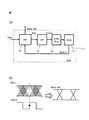
図1は、入力データとクロックとの位相差を検出する位相検出回路(Phase Detector: PD)を利用するCDR回路を示す図であり、(A)がブロック図を示し、(B)が入力データ、クロックおよび出力データの関係を示す。
Before describing the embodiments, a general clock data recovery (CDR) circuit will be described.
FIG. 1 is a diagram showing a CDR circuit using a phase detector (PD) that detects a phase difference between input data and a clock, where (A) shows a block diagram and (B) shows input data. The relationship between clock and output data is shown.
図1の(A)に示すように、CDR回路10は、電圧制御発振器(Voltage Control Oscillator: VCO)11と、位相検出回路(PD)12と、チャージポンプ(CP)13と、ループフィルタ14と、を有する。VCO11は、周波数が可変であれば電圧制御に限定されるものではないが、VCOが広く使用されているので、以下のVCOを使用する例を説明する。VCO11は、クロックCLK−Iを発生し、制御電圧を変化させることによりクロックCLK−Iの周波数が変化する。PD12は、入力データDataとクロックCLK−Iの位相差(クロック位相制御信号)PDIを検出する。後述するように、ここでは、PD12は、ラッチ回路の機能を有し、位相差PDIを検出すると共に、入力データDataをクロックCLK−Iの変化エッジに同期して取り込み、受信データData outとして出力する。CP13は、位相差PDIに従いループフィルタ14に対する電流の足し引きを行い、ループフィルタ14は、位相差PDIに対応する制御電圧を生成する。言い換えれば、CP13およびループフィルタ14は、VCO11の制御部を形成する。VCO11は、制御電圧に応じて発振周波数を変化させる。
As shown in FIG. 1A, the
以上の構成により、VCO11の発振周波数(クロックCLK−Iの周波数)を変化させるフィードバック回路が形成される。このフィードバック回路により、入力データDataとクロックCLK−Iの周波数が一致し、クロックCLK−Iの変化エッジ(立下りエッジ)が入力データDataの変化エッジに一致するように、すなわち位相が一致するように制御される。 With the above configuration, a feedback circuit that changes the oscillation frequency of the VCO 11 (the frequency of the clock CLK-I) is formed. By this feedback circuit, the frequency of the input data Data and the clock CLK-I match, and the change edge (falling edge) of the clock CLK-I matches the change edge of the input data Data, that is, the phase matches. Controlled.
入力データDataおよびクロックCLK−Iの周波数および位相が一致した状態では、クロックCLK−Iの立上りエッジは、入力データDataが変化エッジの中間の位相、すなわちDataが安定した状態に一致する。そこで、クロックCLK−Iの立上りエッジに同期して入力データDataを取り込み、正しい受信データData outを出力する。 In a state where the frequency and phase of the input data Data and the clock CLK-I match, the rising edge of the clock CLK-I matches the phase where the input data Data is in the middle of the changing edge, that is, the state where the data is stable. Therefore, the input data Data is taken in synchronization with the rising edge of the clock CLK-I, and the correct received data Data out is output.
図1の(B)に示すように、入力データDataおよびクロックCLK−Iの周波数および位相が一致した状態でも、入力データDataの信号経路の影響で、入力データDataは、クロックCLK−Iに対して位相が変動するジッタを有する。ジッタがある状態でも、クロックCLK−Iの立上りエッジは、入力データDataが変化エッジの中間の位相の安定した状態に一致するので、正しい受信データData outを取り込み、位相の安定した受信データData outを出力できる。 As shown in FIG. 1B, even when the frequency and phase of the input data Data and the clock CLK-I match, the input data Data is not related to the clock CLK-I due to the influence of the signal path of the input data Data. And jitter with phase variations. Even in the presence of jitter, the rising edge of the clock CLK-I matches the stable state of the phase in the middle of the change edge of the input data Data, so that the correct received data Data out is taken in and the received data Data out with stable phase is output. Can be output.
図2は、位相検出回路(PD)の回路例およびCDR回路における動作を示すタイムチャートであり、(A)がPDの回路例を、(B)がタイムチャートを示す。
図2の(A)に示すように、位相検出回路(PD)は、D型(D−type)フリップフロップ(FF)で形成され、ここでは、入力データDataがD−FFのクロック端子に、クロックCLK−IがD−FFのデータ端子に入力される。このD−FFは、入力データDataが変化した時のクロックCLK−Iの値をラッチして位相差PDIとして出力する。ここでは、入力データDataがD−FFのクロック端子に、クロックCLK−IがD−FFのデータ端子に入力される例を示すが、クロックCLK−IがD−FFのクロック端子に、入力データDataがD−FFのデータ端子に入力される構成も可能である。さらに、入力データDataおよびクロックCLK−Iを単相信号として図示するが、数GHz以上の高速信号については、差動回路で実現されることが望ましい。したがって、図2の(A)のD−FFは、入力データDataの立上りエッジのみでなく、立下りエッジでもクロックCLK−Iをラッチするものとし、これは、以下の説明および他の信号についても同様とする。ただし、実施形態はこれに限定されるものではなく、単相信号でも動作可能である。差動信号の場合には、2個のラッチ回路を使用して反転した入力データDataおよびクロックCLK−Iを入力することにより立上りおよび立下りの両方のエッジでの変化を検出するようにする。
FIG. 2 is a time chart showing a circuit example of the phase detection circuit (PD) and an operation in the CDR circuit, where (A) shows a circuit example of the PD and (B) shows a time chart.
As shown in FIG. 2A, the phase detection circuit (PD) is formed of a D-type flip-flop (FF). Here, the input data Data is input to the clock terminal of the D-FF. The clock CLK-I is input to the data terminal of D-FF. This D-FF latches the value of the clock CLK-I when the input data Data changes and outputs it as a phase difference PDI. In this example, the input data Data is input to the D-FF clock terminal and the clock CLK-I is input to the D-FF data terminal. However, the clock CLK-I is input to the D-FF clock terminal. A configuration in which Data is input to the data terminal of the D-FF is also possible. Furthermore, although the input data Data and the clock CLK-I are illustrated as single-phase signals, it is desirable that a high-speed signal of several GHz or more is realized by a differential circuit. Therefore, the D-FF in FIG. 2A latches the clock CLK-I not only at the rising edge of the input data Data but also at the falling edge. This is also true for the following description and other signals. The same shall apply. However, the embodiment is not limited to this, and can be operated with a single-phase signal. In the case of a differential signal, the input data Data and the clock CLK-I inverted by using two latch circuits are input to detect a change at both rising and falling edges.
図2の(B)のタイムチャートでは、CLK−IがDataに対して位相遅れの場合を左側に、位相進みの場合を中央に、位相が最適(位相一致)の場合を右側に、それぞれ示す。 In the time chart of FIG. 2B, the case where CLK-I is delayed in phase with respect to Data is shown on the left side, the case of phase advance is shown in the center, and the case where the phase is optimal (phase matching) is shown on the right side. .
CLK−IがDataに対して位相遅れの場合、Dataの変化エッジでは、CLK−Iは高(High: H)レベルであり、位相差PDIはHレベルになる。これに応じて、VCO11は、発振周波数を増加させる方向に制御される。
When CLK-I is delayed in phase with respect to Data, CLK-I is at a high (High: H) level and the phase difference PDI is at H level at the changing edge of Data. In response to this, the
CLK−IがDataに対して位相進みの場合、Dataの変化エッジでは、CLK−Iは低(Low: L)レベルであり、位相差PDIはLレベルになる。これに応じて、VCO11は、発振周波数を減少させる方向に制御される。
When CLK-I is advanced in phase with respect to Data, CLK-I is at a low (Low: L) level and the phase difference PDI is at L level at the changing edge of Data. In response to this, the
CLK−IのDataに対する位相が最適の場合、Dataの変化エッジでは、CLK−IはLまたはHと判定されるが、その後逆の判定になるようにVCO11が制御され、このような制御が繰り返されるため、LまたはHと判定される確率が等しくなる。これにより、PDIは、LとHの間で変化し、ループフィルタ14の出力する制御電圧は、LとHの中間レベルになる。図2の(A)では、説明の都合上、PDIとして、LまたはHに交互に変化する波形ではなく、ループフィルタ14で平均化された中間レベルで示している。
When the phase of CLK-I with respect to Data is optimal, at the changing edge of Data, CLK-I is determined to be L or H, but then the
図1の(A)に示したCDR回路は、クロック再生が可能な周波数範囲が狭いという課題があった。そこで、入力データとクロックとの位相差に加えて入力データとクロックとの周波数関係を検出する位相周波数検出(Phase Frequency Detector: PFD)回路を利用するCDR回路が用いられる。 The CDR circuit shown in FIG. 1A has a problem that the frequency range in which clock recovery is possible is narrow. Therefore, a CDR circuit using a phase frequency detector (PFD) circuit that detects the frequency relationship between the input data and the clock in addition to the phase difference between the input data and the clock is used.
図3は、PFD回路を利用するCDR回路を示す図であり、(A)がブロック図を示し、(B)がPFD回路の構成を示すブロック図である。
図3の(A)および(B)に示すように、CDR回路20は、VCO21と、位相周波数検出回路(PFD)22と、CP23と、ループフィルタ24と、を有する。VCO21は、第1クロックCLK−Iに加えて、CLK−Iと同じ周波数で位相の異なる第2クロックCLK−Qを出力する。例えば、CLK−Qは、CLK−Iに対して90度位相が進んでいる。PFD22は、入力データDataとクロックCLK−Iの位相差PDIおよび周波数位相信号FDOを検出する。
3A and 3B are diagrams illustrating a CDR circuit using a PFD circuit. FIG. 3A is a block diagram, and FIG. 3B is a block diagram illustrating a configuration of the PFD circuit.
As shown in FIGS. 3A and 3B, the
図3の(B)に示すように、PFD22は、第1位相検出回路31と、第2位相検出回路32と、周波数位相検出回路33と、を有する。第1位相検出回路31、第2位相検出回路32および周波数位相検出回路33は、例えば、非特許文献1に記載されたものが使用できる。非特許文献1は、2個のサンプルホールド回路(ラッチ回路)およびマルチプレクサで形成される差動型の第1位相検出回路および第2位相検出回路を記載している。また、非特許文献1は、2個のラッチ回路および変形マルチプレクサで形成される差動型の周波数位相検出回路を記載している。
As shown in FIG. 3B, the
第1位相検出回路31は、入力データDataの変化エッジでラッチした第1クロックCLK−Iの値を合成してクロック位相制御信号PDIとして出力する。クロック位相制御信号PDIは、Dataの変化エッジに対してCLK−Iの変化エッジが進んでいるか、遅れているかを示す。第2位相検出回路32は、Dataの変化エッジでラッチした第2クロックCLK−Qの値を合成してクロック位相検出信号PDQとして出力する。クロック位相検出信号PDQは、Dataの変化エッジに対してCLK−Qの変化エッジが進んでいるか、遅れているかを示す。
The first
周波数位相検出回路33は、PDIの変化エッジの方向およびPDIの変化エッジでラッチしたPDQの値から、CLK−Iの周波数がDataの周波数に対して小さいかまたは大きいかを示す周波数位相信号FDOを生成する。FDOは、CLK−Iの周波数がDataの周波数に対して小さい時に+1、大きい時に−1、同じ時に0を示す。クロック位相制御信号PDIおよび周波数位相信号FDOは、チャージポンプ23に供給される。これにより、VCO21の制御は、クロック位相制御信号PDIおよび周波数位相信号FDOに基づいて行われる。
The frequency
図4は、図3の(B)のPFDの各部の動作を示すタイムチャートであり、(A)が入力データDataと第1クロックCLK−Iの周波数が異なる非ロック状態(アンロック状態)の波形を、(B)が周波数および位相が一致したロック状態の波形を示す。 FIG. 4 is a time chart showing the operation of each part of the PFD in FIG. 3B, where FIG. 4A shows an unlocked state (unlocked state) in which the frequencies of the input data Data and the first clock CLK-I are different. A waveform (B) shows a waveform in a locked state in which the frequency and the phase coincide with each other.
図4の(A)に示すように、DataとCLK−Iの周波数が異なるアンロック状態では、クロック位相制御信号PDIおよびクロック位相検出信号PDQの両方が変化し、周波数位相信号FDOも変化する。図4の(A)は、CLK−Iの周波数がDataの周波数より小さい状態であり、図示のように、FDOは、0と+1の間でPDIと逆相で変化する。CLK−Iの周波数がDataの周波数より大きい状態の時には、FDOは0と−1の間で変化する。チャージポンプ23およびループフィルタ24により、PDIとFDOを1:1で合成したPDI+FDOが制御信号として生成される場合、PDI+FDOは、0と+1の間で変化し、VCO21の発振周波数を増加させる。なお、制御信号は、PDI+FDOに限定されず、合成の重み付けを異ならせる場合もある。
As shown in FIG. 4A, in the unlock state where the frequencies of Data and CLK-I are different, both the clock phase control signal PDI and the clock phase detection signal PDQ change, and the frequency phase signal FDO also changes. FIG. 4A shows a state where the frequency of CLK-I is smaller than the frequency of Data, and as shown in the figure, FDO changes between 0 and +1 in a phase opposite to PDI. When the frequency of CLK-I is higher than the frequency of Data, FDO changes between 0 and -1. When PDI + FDO obtained by combining PDI and FDO at 1: 1 by the
図4の(B)に示すように、DataとCLK−Iの周波数および位相が一致した状態では、クロック位相制御信号PDIは変化するが、クロック位相検出信号PDQは所定値(−1)に固定される。そのため、周波数位相信号FDOはゼロになる。したがって、PDI+FDOはPDIになり、VCO21の制御は、周波数位相信号FDOを使用せず、クロック位相制御信号PDIのみを使用する制御が行われる。
As shown in FIG. 4B, when the frequency and phase of Data and CLK-I match, the clock phase control signal PDI changes, but the clock phase detection signal PDQ is fixed at a predetermined value (−1). Is done. Therefore, the frequency phase signal FDO becomes zero. Therefore, PDI + FDO becomes PDI, and control of the
CDR回路は、消費電力の低減が求められている。上記のように、ロック状態では周波数位相信号はゼロになり、VCOの制御に影響しないにもかかわらず、周波数位相信号を検出する回路は動作しており、その回路の消費電力が無駄である。CDR回路では、実際の動作では大部分がロック状態であり、ロック状態で周波数位相検出回路を停止すれば消費電力を低減することができると考えられる。 The CDR circuit is required to reduce power consumption. As described above, the frequency phase signal is zero in the locked state, and the circuit for detecting the frequency phase signal is operating even though it does not affect the control of the VCO, and the power consumption of the circuit is useless. Most of the CDR circuits are in a locked state in actual operation, and it is considered that power consumption can be reduced by stopping the frequency phase detection circuit in the locked state.
しかし、周波数位相検出回路を停止した場合、位相検出回路のみを使用するCDR回路となり、クロック再生が可能な周波数範囲が狭く、ロック状態から非ロック状態に変化したことが検出できず、非ロック時に周波数位相検出回路を再び起動することができないという問題がある。 However, when the frequency phase detection circuit is stopped, it becomes a CDR circuit that uses only the phase detection circuit, the frequency range in which the clock can be reproduced is narrow, and it cannot be detected that the lock state has changed to the non-lock state. There is a problem that the frequency phase detection circuit cannot be started again.
これまで、位相検出回路の出力するクロック位相制御信号PDIに基づいてロック状態であるか非ロック状態であるかを検出することは行われていなかった。
以下に説明する実施形態の信号再生回路では、ロック状態から非ロック状態に変化したことを、周波数位相検出回路によらず検出する。
Until now, it has not been detected whether the locked state or the unlocked state is based on the clock phase control signal PDI output from the phase detection circuit.
In the signal reproduction circuit according to the embodiment described below, the change from the locked state to the unlocked state is detected regardless of the frequency phase detection circuit.
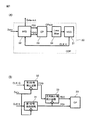
図5は、第1実施形態の信号再生(Clock Data Recovery : CDR)回路を示す図であり、(A)がブロック図を示し、(B)がCDR回路の起動時の動作を示すタイムチャートである。
第1実施形態のCDR回路は、電圧制御発振器(VCO)41と、第1位相検出回路42と、第2位相検出回路43と、周波数位相検出回路44と、チャージポンプ(CP)46と、ループフィルタ47と、を有する。第1実施形態のCDR回路は、さらに、PD−Iフィルタ(filter)回路51と、振幅検出回路52と、判定回路53と、を有する。VCO41、第1位相検出回路42、第2位相検出回路43、周波数位相検出回路44、CP47およびループフィルタ48は、図3の対応する要素と同じものが利用可能であるが、それに限定されるものではない。
5A and 5B are diagrams showing a signal recovery (Clock Data Recovery: CDR) circuit according to the first embodiment. FIG. 5A is a block diagram, and FIG. 5B is a time chart showing an operation when the CDR circuit is activated. is there.
The CDR circuit of the first embodiment includes a voltage controlled oscillator (VCO) 41, a first
VCO41は、第1クロックCLK−IおよびCLK−Iと同じ周波数で位相の異なる第2クロックCLK−Qを発生し、制御電圧を変化させることによりCLK−IおよびCLK−Qの周波数を変化させる。CLK−Qは、CLK−Iに対して90度位相が進んでいる。
The
第1位相検出回路42は、入力データDataの変化エッジでラッチした第1クロックCLK−Iの値を合成してクロック位相制御信号PDIとして出力する。クロック位相制御信号PDIは、Dataの変化エッジに対してCLK−Iの変化エッジが進んでいるか、遅れているかを示す。第2位相検出回路43は、Dataの変化エッジでラッチした第2クロックCLK−Qの値を合成してクロック位相検出信号PDQとして出力する。クロック位相検出信号PDQは、Dataの変化エッジに対してCLK−Qの変化エッジが進んでいるか、遅れているかを示す。周波数位相検出回路44は、PDIの変化エッジの方向およびPDIの変化エッジでラッチしたPDQの値から、CLK−Iの周波数がDataの周波数に対して小さいかまたは大きいかを示す周波数位相信号FDOを生成する。FDOは、CLK−Iの周波数がDataの周波数に対して小さい時に+1、大きい時に−1、同じ時に0を示す。第1位相検出回路42、第2位相検出回路43および周波数位相検出回路44は、例えば、非特許文献1に記載された差動型の回路で実現される。
The first
CP46は、周波数差状態においてはPDIおよびFDOに従いループフィルタ47に対する電流の足し引きを行い、正常ロック状態および逆相ロック状態においては、PDIに従いループフィルタ47に対する電流の足し引きを行う。ループフィルタ47は、電流の足し引きにより制御電圧を生成し、VCO41に供給する。
The
PD−Iフィルタ(filter)回路51は、クロック位相制御信号PDIの高周波成分を除去し、低周波成分を含むPDI filを出力する。
図6は、PD−Iフィルタ(filter)回路51の構成例を示す図である。図6のフィルタ回路は、抵抗と容量素子からなる広く知られたフィルタ回路であり、差動信号であるので、2つの類似の第1および第2フィルタ回路を有する。第1フィルタ回路は、正極性の信号+PDIを入力とし、フィルタリングされた正極性の+PDI filを出力する。第2フィルタ回路は、負極性の信号−PDIを入力とし、フィルタリングされた負極性の−PDI filを出力する。
The PD-
FIG. 6 is a diagram illustrating a configuration example of the PD-
振幅検出回路52は、PD−Iフィルタ回路51の出力するPDI filの振幅を検出し、振幅信号PDI modを出力する。
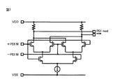
図7は、振幅検出回路52の構成例を示す図である。図7の振幅検出回路は、差動入力+PDI filと−PDI filの掛け算(2乗演算)を行う広く知られた演算回路である。差動入力+PDI filおよび−PDI filは、振幅が大きい時には+1または−1を示し、振幅が小さい時には0を示す。したがって、振幅が大きい+1または−1の時には、振幅信号PDI mod=1となり、振幅が小さい0の時には振幅信号PDI mod=0となる。
The
FIG. 7 is a diagram illustrating a configuration example of the
判定回路53は、振幅検出回路52の出力する振幅信号PDI modを閾値Vthと比較し、判定結果CLKQ dnを出力する。判定結果CLKQ dnは、振幅が大きい時、すなわちVthより大きい時には0に、振幅が小さい時、すなわちVthより小さい時には1になる。
The
以上の構成により、入力データDataの周波数に第1クロックCLK−Iの周波数が一致し、Dataの変化エッジにCLK−Iの立下りエッジが同期するフィードバック制御系が形成される。すなわち、第1位相検出回路42、第2位相検出回路43、周波数位相検出回路44、CP46、ループフィルタ47、PD−Iフィルタ(filter)回路51、振幅検出回路52および判定回路53は、VCO41を制御するフィードバック制御回路を形成する。さらに、第1位相検出回路42、第2位相検出回路43および周波数位相検出回路44は、DataとCLK−Iの位相関係および周波数関係を検出する位相周波数検出器(Phase Frequency Detector: PFD)を形成する。また、PD−Iフィルタ(filter)回路51、振幅検出回路52および判定回路53は、CDR回路がロック状態であるか非ロック状態(周波数差状態)であるかを検出する状態検出回路を形成する。
With the above configuration, a feedback control system is formed in which the frequency of the first clock CLK-I matches the frequency of the input data Data, and the falling edge of the CLK-I is synchronized with the changing edge of the Data. That is, the first
図5の(B)では、VCO41の発振周波数(CLK−Iの周波数)の変化を上側に、CLKQ dnの変化を下側に示す。
In FIG. 5B, the change of the oscillation frequency (CLK-I frequency) of the
CDR回路が起動すると、VCO41の発振周波数は、フィードバック制御により自走周波数から単調に増加する。VCO41の発振周波数が、Dataの周波数であるロック周波数の前後の所定範囲(PDIのトラッキング範囲)にまで増加し、それを状態検出回路が検出すると、CLKQ dnは1に変化する。自走周波数からPDIのトラッキング範囲までのVCO41の発振周波数の変化範囲が周波数差(FD)動作による周波数引込範囲である。PFDを使用することにより、PDを使用する場合に比べて、周波数引込範囲を大きくできる。ロック状態では、VCO41の発振周波数は、フィードバック制御により、ロック周波数に一致するように、増減を繰り返す。
When the CDR circuit is activated, the oscillation frequency of the
図8は、第1実施形態のCDR回路の各部の動作波形である。図8では、CDR回路が起動し、ロック状態になりその状態を保持する場合のVCO41の制御信号VCO cnf、PDI、PDI fil、PDI modおよびCLKQ dnの動作波形が示される。
FIG. 8 is an operation waveform of each part of the CDR circuit of the first embodiment. FIG. 8 shows operation waveforms of the control signals VCO cnf, PDI, PDI file, PDI mod, and CLKQ dn of the
CDR回路の起動後、VCO41は、発振周波数を自走周波数から増加させる。VCO cntは、VCO41の発振周波数が周波数引込範囲になると、比較的大きな振幅で且つ低周波数で増減を繰り返し、徐々に中心レベルが上昇し、変化信号の周波数は徐々に減少する。そして、VCO41の発振周波数が同期周波数範囲になると、VCO cntは、一定レベルを中心として小さな振幅で且つ高周波数で変化する状態になる。
After the activation of the CDR circuit, the
一方、VCO41の発振周波数が周波数引込範囲になると、CLK−IとDataのエッジは、ある程度位相が近づいた状態になり、位相差がゼロになる方向にフィードバック制御される。さらに発振周波数が同期周波数範囲になると、CLK−IとDataのエッジはほぼ一致し、フィードバック制御により位相の進みと遅れが繰り返される。そのため、PDIは、周波数引込範囲にある状態(周波数差状態)では比較的低周波で変化し、徐々に周波数が小さくなるように変化し、同期周波数範囲になると、高周波で変化する状態が繰り返される。これがロック状態である。
On the other hand, when the oscillation frequency of the
したがって、PDIから高周波成分を除去した低周波成分の信号PDI filは、図8に示すように、周波数引込範囲にある状態では、比較的低周波で変化し、同期周波数範囲になると中間レベルの一定の信号になる。そのため、PDI filの振幅信号PDI modは、周波数引込範囲にある状態では高レベルの信号になり、同期周波数範囲になると低レベルに変化する。そのため、CLKQ dnは、周波数引込範囲にある状態では低レベルであり、同期周波数範囲になると高レベルに変化する。 Therefore, as shown in FIG. 8, the low-frequency component signal PDI file obtained by removing the high-frequency component from the PDI changes at a relatively low frequency in the frequency pull-in range, and has a constant intermediate level in the synchronous frequency range. Signal. For this reason, the amplitude signal PDI mod of the PDI file becomes a high level signal when in the frequency pull-in range, and changes to a low level when in the synchronous frequency range. Therefore, CLKQ dn is at a low level when in the frequency pull-in range, and changes to a high level when in the synchronous frequency range.
以上説明したように、第1実施形態のCDR回路では、PD−Iフィルタ(filter)回路51、振幅検出回路52および判定回路53を含む状態検出回路が、CDR回路がロック状態であるか非ロック状態(周波数引込範囲にある状態)であるかを検出する。
なお、状態検出回路は、第2位相検出回路43および周波数位相検出回路44が無い場合にも有効であり、第1位相検出回路42の出力するクロック位相制御信号PDIに基づいてロック状態であるか非ロック状態であるかを検出することができる。
As described above, in the CDR circuit of the first embodiment, the state detection circuit including the PD-
The state detection circuit is effective even when the second
図9は、第2実施形態の信号再生(Clock Data Recovery : CDR)回路のブロック図である。
第2実施形態のCDR回路は、周波数位相検出回路44とCP46の間にスイッチ45を設けたことが第1実施形態のCDR回路と異なり、他の部分は同じである。
FIG. 9 is a block diagram of a signal recovery (Clock Data Recovery: CDR) circuit of the second embodiment.
The CDR circuit of the second embodiment is different from the CDR circuit of the first embodiment in that a
スイッチ45は、判定回路53が出力するCLKQ dnに応じて、周波数位相検出回路44が出力する周波数位相信号FDOを、CP47に供給するか否かを切り替える。具体的には、非ロック状態(周波数引込範囲にある状態)、すなわち周波数差(FD)状態においてはFDOをCP47に供給し、ロック状態においては、FDOをCP47に供給しないように切り替える。ここでは、スイッチ45からCP46に供給される信号を、FDSで表す。したがって、FD−cntは、周波数差状態においてはFDOであり、ロック状態では、CP46に影響しない固定値(例えば0)である。
The
CP46は、周波数差状態においてはPDIおよびFDSに従いループフィルタ47に対する電流の足し引きを行い、ロック状態においては、PDIに従いループフィルタ47に対する電流の足し引きを行う。ループフィルタ47は、電流の足し引きにより制御電圧を生成し、VCO41に供給する。
The
ロック状態であっても、ジッタの大きい信号受信時には周波数位相信号が変動し、周波数位相検出回路44が動作し、入力データと第1クロックの周波数が不一致であることを示す周波数位相信号を出力することが起こり得る。このような周波数位相信号がチャージポンプ46に入力されると、VCOの制御が一時的に変化し、第1クロックの周波数が入力データの周波数と異なることを示す同期外れ(非ロック)エラーが発生する。しかし、第2実施形態のCDR回路では、ジッタの大きい信号受信により周波数位相検出回路44が周波数の不一致を示す周波数位相信号FDOを発生しても、直ちにチャージポンプ46に入力されることは無く、同期外れエラーは発生しない。もちろん、アンロック状態になった時には、CLKQ dnがアンロック状態を示す値に変化し、スイッチ45が導通して周波数位相信号がチャージポンプ46に入力され、広い周波数引込範囲が実現される。
Even in the locked state, the frequency phase signal fluctuates when a signal with a large jitter is received, and the frequency
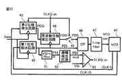
図10は、第3実施形態の信号再生(Clock Data Recovery : CDR)回路のブロック図である。
第3実施形態のCDR回路は、第2位相検出回路43、周波数位相検出回路44およびスイッチ45をCLKQ dnに応じてオフすることが第2実施形態のCDR回路と異なり、他は同じである。CLKQ dnがアンロック状態を示す時、第2位相検出回路43および周波数位相検出回路44は動作状態となり、スイッチ45は導通する。CLKQ dnがロック状態を示す時、第2位相検出回路43および周波数位相検出回路44は非動作状態になり、スイッチ45は遮断する。
FIG. 10 is a block diagram of a signal recovery (Clock Data Recovery: CDR) circuit of the third embodiment.
The CDR circuit of the third embodiment is the same as the CDR circuit of the second embodiment except that the second
第3実施形態のCDR回路は、ジッタの大きい信号受信による同期外れエラーが発生しないという第2実施形態のCDR回路と同様の効果を有すると共に、第2位相検出回路43および周波数位相検出回路44を停止するので消費電力を低減できる。第3実施形態のCDR回路では、ロック状態になるまでは第2位相検出回路43および周波数位相検出回路44が動作して広い周波数引込範囲を実現するが、一旦ロック状態なると周波数位相信号FDOは使用されない状態になる。したがって、第2位相検出回路43および周波数位相検出回路44により周波数位相信号FDOが発生されなくても特に問題はない。実際のCDR回路の動作では、ロック状態が大きな割合を占めており、ロック状態で第2位相検出回路43および周波数位相検出回路44の動作を停止することにより、大きな消費電力の低減効果が得られる。例示のCDR回路では、約20%の消費電力削減が実現された。
The CDR circuit of the third embodiment has the same effect as that of the CDR circuit of the second embodiment in that an out-of-synchronization error due to reception of a signal with large jitter does not occur, and the second
第3実施形態のCDR回路は、ロック状態からアンロック状態に変化した時には、CLKQ dnがアンロック状態を示す値に変化し、それに応じて第2位相検出回路43および周波数位相検出回路44の動作状態になり、スイッチ45が導通する。これにより、周波数位相信号がチャージポンプ46に入力されるので、広い周波数引込範囲が実現される。
In the CDR circuit of the third embodiment, when the lock state is changed to the unlock state, the CLKQ dn changes to a value indicating the unlock state, and the operations of the second
第3実施形態のCDR回路では、クロック位相制御信号PDIとクロック位相検出信号PDQを用いて周波数位相信号FDOを生成する構成を示したが、ロック状態ではクロック位相制御信号PDIのみで動作し、アンロック状態では周波数同期の回路を動作させるCDR回路であれば、第3実施形態のCDR回路の構成に限らず、他の構成のCDRでも広い周波数引込範囲と、ロック状態では位相制御信号PDIのみでの動作を実現することが可能である。 In the CDR circuit of the third embodiment, the configuration in which the frequency phase signal FDO is generated using the clock phase control signal PDI and the clock phase detection signal PDQ has been shown. However, in the locked state, only the clock phase control signal PDI operates. A CDR circuit that operates a frequency-synchronized circuit in the locked state is not limited to the configuration of the CDR circuit of the third embodiment, but a CDR can be configured in other configurations with a wide frequency pull-in range, and in the locked state, only the phase control signal PDI. It is possible to realize the operation.
以上説明した第1から第3実施形態のCDR回路では、PD−Iフィルタ(filter)回路51は、クロック位相制御信号PDIの高周波成分を除去して低周波成分を出力するローパスフィルタであったが、ハイパスフィルタを使用することも可能である。図8に示したように、PDIは、アンロック状態(周波数検出中)では比較的低周波の成分を主とし、ロック状態では比較的高周波の成分を主とする。そこで、PD−Iフィルタ(filter)回路51がハイパスフィルタであると、PDI filは、アンロック状態(周波数検出中)では小さな振幅の中間レベルの信号となり、ロック状態では大きな振幅の高周波信号となる。したがって、その振幅信号PDI modは、アンロック状態(周波数検出中)では小さく、ロック状態では大きくなり、閾値に対して第1から第3実施形態と逆論理で比較すると、CLK dnは、第1から第3実施形態と同じ信号になる。
In the CDR circuits of the first to third embodiments described above, the PD-
図11は、ハイパスフィルタ、バンドパスフィルタおよびバンドパスフィルタの周波数特性を示す図であり、(A)がハイパスフィルタの回路図を、(B)がバンドパスフィルタの回路図を、(C)が周波数特性を示す。 11A and 11B are diagrams illustrating frequency characteristics of the high-pass filter, the band-pass filter, and the band-pass filter. FIG. 11A is a circuit diagram of the high-pass filter, FIG. 11B is a circuit diagram of the band-pass filter, and FIG. Shows frequency characteristics.
図11の(A)のハイパスフィルタは、容量素子と抵抗からなる広く知られたフィルタである。もし、差動信号が使用される場合には、図6に示したように図11の(A)のフィルタ回路を2個使用する。 The high-pass filter shown in FIG. 11A is a well-known filter including a capacitive element and a resistor. If a differential signal is used, two filter circuits shown in FIG. 11A are used as shown in FIG.
図8に示したように、クロック位相制御信号PDIは、高周波に比較して低周波の信号であるが、ある程度の以上の周波数を有する信号であり、雑音を除去する上では直流成分を含むある程度以下の低周波成分は抽出しないことが望ましい。そこで、第1から第3実施形態のPD−Iフィルタ(filter)回路51として、バンドパスフィルタを使用し、PDIのある周波数帯域の成分を抽出するようにしてもよい。
As shown in FIG. 8, the clock phase control signal PDI is a signal having a frequency lower than that of the high frequency, but is a signal having a frequency higher than a certain level, and includes a DC component to remove noise. It is desirable not to extract the following low frequency components. Therefore, a bandpass filter may be used as the PD-
図11の(B)のバンドパスフィルタは、ハイパスフィルタとローパスフィルタを直列に接続した構成を有する。例えば、ハイパスフィルタは、図11の(C)において破線で示す特性、すなわち100MHz以上の周波数成分を通過させる特性を有する。ローパスフィルタは、図11の(C)において実線で示す特性、すなわち2GHz以下の周波数成分を通過させる特性を有する。したがって、バンドパスフィルタは、100MHz以上2GHz以下の周波数成分を通過させる。 The band pass filter in FIG. 11B has a configuration in which a high pass filter and a low pass filter are connected in series. For example, the high-pass filter has a characteristic indicated by a broken line in FIG. 11C, that is, a characteristic that allows a frequency component of 100 MHz or more to pass. The low-pass filter has a characteristic indicated by a solid line in FIG. 11C, that is, a characteristic that allows a frequency component of 2 GHz or less to pass. Therefore, the band pass filter passes a frequency component of 100 MHz to 2 GHz.
図12は、第4実施形態のCDR回路を示す図である。図12の(A)は、第1および第2位相検出回路、周波数位相検出回路、CP、PD−Iフィルタ(filter)回路と、振幅検出回路および判定回路の部分の構成を示す回路ブロック図である。図12の(B)は、第1位相検出回路の回路例を示す。 FIG. 12 is a diagram illustrating a CDR circuit according to the fourth embodiment. FIG. 12A is a circuit block diagram showing configurations of the first and second phase detection circuits, the frequency phase detection circuit, the CP, the PD-I filter circuit, the amplitude detection circuit, and the determination circuit. is there. FIG. 12B shows a circuit example of the first phase detection circuit.
第4実施形態のCDR回路は、図5の第1実施形態のCDR回路と類似の構成を有し、第1位相検出回路および第2位相検出回路の構成のみが異なり、他は第1実施形態と同じである。第1位相検出回路81は、第1クロックCLK−Iをトリガとして、CLK−Iの変化エッジに対する入力データDataの位相を検出する。第2位相検出回路82は、CLK−Iと同じ周波数を有し、位相が90度進んだ第2クロックCLK−Qをトリガとして、CLK−Qの変化エッジに対する入力データDataの位相を検出する。
The CDR circuit of the fourth embodiment has a configuration similar to that of the CDR circuit of the first embodiment of FIG. 5, except for the configurations of the first phase detection circuit and the second phase detection circuit, and the others are the first embodiment. Is the same. The first
図12の(B)に示すように、第1位相検出回路81は、インバータ83と、第1フリップフロップ(FF)84と、第2FF85と、マルチプレクサ(MUX)86と、を有する。インバータ83は、CLK−Iを反転して/CLK−Iを出力する。第1FF84は、Dataを入力とし、/CLK−IをトリガとするFFで、/CLK−Iの立上りエッジにおけるDataの値をラッチし、sample1として出力する。第2FF85は、Dataを入力とし、CLK−IをトリガとするFFで、CLK−Iの立上りエッジにおけるDataの値をラッチし、sample2として出力する。MUX86は、sample1およびsample2を合成し、クロック位相制御信号PDIを生成する。
As shown in FIG. 12B, the first
第2位相検出回路82は、図12の(B)に示す構成を有するが、CLK−Iの代わりにCLK−Qが入力され、クロック位相検出信号PDQを出力することが異なる。
The second
Data、CLK−IおよびCLK−Qが差動信号である場合には、図12の(B)の位相検出回路は、例えば、非特許文献1に記載された位相検出器PDのように実現される。
When Data, CLK-I, and CLK-Q are differential signals, the phase detection circuit in FIG. 12B is realized as the phase detector PD described in
第4実施形態の構成は、第2および第3実施形態にも適用可能であり、その他の動作および効果は第1から第3実施形態と同じであり、説明を省略する。 The configuration of the fourth embodiment can be applied to the second and third embodiments, and the other operations and effects are the same as those of the first to third embodiments, and the description thereof is omitted.
以上、第1から第4実施形態の信号再生(CDR)回路について説明したが、次に、実施形態のCDR回路を使用する装置について説明する。 The signal reproduction (CDR) circuit of the first to fourth embodiments has been described above. Next, an apparatus using the CDR circuit of the embodiment will be described.
図13は、実施形態のCDR回路を使用する光通信システムの構成を示す図である。
光通信システムは、送信信号を光信号に変換して出力する送信機100と、送信機100からの光信号を伝送する光ファイバ200と、光信号を受けて受信信号を再生する受信機300と、を有する。送信機100は、電子装置等から送信された送信信号を再生して光信号を生成する。また、送信機100は、光ファイバを介して受信した光信号を一旦電気信号に変換した後、再度光信号に変換して出力する中継装置でもよい。受信機300は、再生した受信信号を電気信号として電子装置等に出力する。また、受信機300は、受信信号を再度光信号に変換して出力する中継装置でもよい。
FIG. 13 is a diagram illustrating a configuration of an optical communication system using the CDR circuit of the embodiment.
The optical communication system includes a
送信機100は、信号再生(CDR)回路101と、ドライバ(Driver)102と、レーザダイオード(LD)103と、を有する。信号再生(CDR)回路101は、受信したデータ信号からクロックを再生すると共に送信データ信号を再生する。ドライバ102は、送信データ信号に応じてLD103を駆動し、光信号を生成して光ファイバ200に出力する。
The
受信機300は、フォトダイオード(PD)301と、トランスインピーダンス増幅器(TIA)302と、信号再生(CDR)回路303と、を有する。PD301は、光ファイバ200から受信した光信号を電気的な受信データ信号に変換する。TIA302は、受信データ信号を増幅する。CDR回路303は、受信データ信号からクロックを再生すると共に受信データ信号を再生する。
The
実施形態の信号再生(CDR)回路は、図21の信号再生(CDR)回路101および303として使用される。
なお、実施形態の信号再生(CDR)回路は、光通信システムに利用可能なだけでなく、電子装置の内外で、クロックに同期して変調したデータ信号の送受信を行う回路で、データ信号からクロックを再生する場合には、どのような回路にも適用可能である。例えば、集積回路チップ内、チップ間(装置内、装置間)で信号を送受信する高速I/Oの分野等のビットレートの一層の高速化が望まれている分野で使用可能である。
The signal reproduction (CDR) circuit of the embodiment is used as the signal reproduction (CDR)
The signal regeneration (CDR) circuit of the embodiment is not only applicable to an optical communication system, but also a circuit that transmits and receives a data signal modulated in synchronization with a clock inside and outside an electronic device. Can be applied to any circuit. For example, the present invention can be used in fields where higher bit rates are desired, such as in the field of high-speed I / O for transmitting and receiving signals within an integrated circuit chip and between chips (inside and between devices).
以上、実施形態を説明したが、ここに記載したすべての例や条件は、発明および技術に適用する発明の概念の理解を助ける目的で記載されたものである。特に記載された例や条件は発明の範囲を制限することを意図するものではなく、明細書のそのような例の構成は発明の利点および欠点を示すものではない。発明の実施形態を詳細に記載したが、各種の変更、置き換え、変形が発明の精神および範囲を逸脱することなく行えることが理解されるべきである。 The embodiment has been described above, but all examples and conditions described herein are described for the purpose of helping understanding of the concept of the invention applied to the invention and technology. In particular, the examples and conditions described are not intended to limit the scope of the invention, and the construction of such examples in the specification does not indicate the advantages and disadvantages of the invention. Although embodiments of the invention have been described in detail, it should be understood that various changes, substitutions and modifications can be made without departing from the spirit and scope of the invention.
41 電圧制御発振器(VCO)
42 第1位相検出回路
43 第2位相検出回路
44 周波数位相検出回路
45 スイッチ
46 チャージポンプ(CP)
47 ループフィルタ
51 PD−Iフィルタ(filter)回路
52 振幅検出回路
53 判定回路
41 Voltage controlled oscillator (VCO)
42 First
47
Claims (12)
入力データと前記第1クロックの位相関係に応じて、前記入力データと前記第1クロックが同期するように前記発振器を制御するフィードバック回路と、を有し、
前記フィードバック回路は、
前記入力データと前記第1クロックの位相関係に応じて前記発振器を制御する制御部と、
前記入力データと前記第1クロックの位相関係に応じてクロック位相制御信号を生成する第1位相検出回路と、
前記クロック位相制御信号の高周波成分または低周波数成分の振幅の大きさからロック状態であるか非ロック状態であるかを検出する状態検出回路と、を有することを特徴とする信号再生回路。 An oscillator that generates a first clock having a variable frequency;
A feedback circuit for controlling the oscillator so that the input data and the first clock are synchronized according to a phase relationship between the input data and the first clock;
The feedback circuit includes:
A control unit for controlling the oscillator according to a phase relationship between the input data and the first clock;
A first phase detection circuit that generates a clock phase control signal according to a phase relationship between the input data and the first clock;
And a state detection circuit for detecting whether the clock phase control signal is in a locked state or in an unlocked state based on the magnitude of the amplitude of the high-frequency component or low-frequency component of the clock phase control signal.
前記フィードバック回路は、
前記入力データと前記第2クロックとの位相関係に応じてクロック位相検出信号を生成する第2位相検出回路と、
前記クロック位相制御信号と前記クロック位相検出信号を比較し、前記入力データと前記第1クロックの周波数関係を示す周波数位相信号を生成する周波数位相検出回路と、を有し、
前記制御部は、前記クロック位相制御信号および前記周波数位相信号に応じて前記発振器を制御することを特徴とする請求項1に記載の信号再生回路。 The oscillator generates a second clock having the same frequency and a different phase as the first clock;
The feedback circuit includes:
A second phase detection circuit that generates a clock phase detection signal in accordance with a phase relationship between the input data and the second clock;
A frequency phase detection circuit that compares the clock phase control signal and the clock phase detection signal and generates a frequency phase signal indicating a frequency relationship between the input data and the first clock;
The signal reproduction circuit according to claim 1, wherein the control unit controls the oscillator according to the clock phase control signal and the frequency phase signal.
前記ロック状態の時に前記第2位相検出回路および前記周波数位相検出回路を非動作状態とし、
前記非ロック状態の時に前記第2位相検出回路および前記周波数位相検出回路を動作状態とする請求項3に記載の信号再生回路。 The feedback circuit includes:
When the locked state, the second phase detection circuit and the frequency phase detection circuit are inoperative,
The signal reproduction circuit according to claim 3, wherein the second phase detection circuit and the frequency phase detection circuit are in an operating state when in the unlocked state.
前記クロック位相制御信号から低周波数成分を抽出するローパスフィルタと、
前記ローパスフィルタの出力する信号の振幅を検出する振幅検出回路と、
前記振幅検出回路の出力する振幅値が、所定レベル以上である時に前記非ロック状態であると判定し、前記所定レベル以下である時に前記ロック状態であると判定する判定回路と、を有する請求項1から5のいずれか1項に記載の信号再生回路。 The state detection circuit includes:
A low pass filter for extracting a low frequency component from the clock phase control signal;
An amplitude detection circuit for detecting the amplitude of the signal output from the low-pass filter;
And a determination circuit that determines that the unlocked state is detected when an amplitude value output from the amplitude detection circuit is equal to or higher than a predetermined level, and determines that the locked state is determined when the amplitude value is equal to or lower than the predetermined level. 6. The signal regeneration circuit according to any one of 1 to 5.
前記クロック位相制御信号から高周波数成分を抽出するハイパスフィルタと、
前記ハイパスフィルタの出力する信号の振幅を検出する振幅検出回路と、
前記振幅検出回路の出力する振幅値が、所定レベル以上である時に前記ロック状態であると判定し、前記所定レベル以下である時に前記非ロック状態であると判定する判定回路と、を有する請求項1から5のいずれか1項に記載の信号再生回路。 The state detection circuit includes:
A high pass filter for extracting a high frequency component from the clock phase control signal;
An amplitude detection circuit for detecting the amplitude of the signal output from the high-pass filter;
And a determination circuit that determines that the lock state is established when an amplitude value output from the amplitude detection circuit is equal to or higher than a predetermined level, and determines that the lock state is not locked when the amplitude value is equal to or lower than the predetermined level. 6. The signal regeneration circuit according to any one of 1 to 5.
前記クロック位相制御信号から下限と上限の間の周波数成分を抽出するバンドパスフィルタと、
前記バンドパスフィルタの出力する信号の振幅を検出する振幅検出回路と、
前記振幅検出回路の出力する振幅値が、所定レベル以上である時に前記非ロック状態であると判定し、前記所定レベル以下である時に前記ロック状態であると判定する判定回路と、を有する請求項1から5のいずれか1項に記載の信号再生回路。 The state detection circuit includes:
A bandpass filter that extracts a frequency component between a lower limit and an upper limit from the clock phase control signal;
An amplitude detection circuit for detecting the amplitude of the signal output from the bandpass filter;
And a determination circuit that determines that the unlocked state is detected when an amplitude value output from the amplitude detection circuit is equal to or higher than a predetermined level, and determines that the locked state is determined when the amplitude value is equal to or lower than the predetermined level. 6. The signal regeneration circuit according to any one of 1 to 5.
前記信号再生回路は、
周波数が可変の第1クロックを発生する発振器と、
入力データと前記第1クロックの位相関係に応じて、前記入力データと前記第1クロックが同期するように前記発振器を制御するフィードバック回路と、を有し、
前記フィードバック回路は、
前記入力データと前記第1クロックの位相関係に応じて前記発振器を制御する制御部と、
前記入力データと前記第1クロックの位相関係に応じてクロック位相制御信号を生成する第1位相検出回路と、
前記クロック位相制御信号の高周波成分または低周波数成分の振幅の大きさからロック状態であるか非ロック状態であるかを検出する状態検出回路と、を有することを特徴とする電子装置。 An electronic device having a signal regeneration circuit that regenerates a clock from received input data and captures the input data by the regenerated clock,
The signal regeneration circuit includes:
An oscillator that generates a first clock having a variable frequency;
A feedback circuit for controlling the oscillator so that the input data and the first clock are synchronized according to a phase relationship between the input data and the first clock;
The feedback circuit includes:
A control unit for controlling the oscillator according to a phase relationship between the input data and the first clock;
A first phase detection circuit that generates a clock phase control signal according to a phase relationship between the input data and the first clock;
An electronic device, comprising: a state detection circuit that detects whether the clock phase control signal is in a locked state or an unlocked state based on a magnitude of an amplitude of a high-frequency component or a low-frequency component of the clock phase control signal.
前記フィードバック回路は、
前記入力データと前記第2クロックとの位相関係に応じてクロック位相検出信号を生成する第2位相検出回路と、
前記クロック位相制御信号と前記クロック位相検出信号を比較し、前記入力データと前記第1クロックの周波数関係を示す周波数位相信号を生成する周波数位相検出回路と、を有し、
前記制御部は、前記クロック位相制御信号および前記周波数位相信号に応じて前記発振器を制御することを特徴とする請求項9に記載の電子装置。 The oscillator generates a second clock having the same frequency and a different phase as the first clock;
The feedback circuit includes:
A second phase detection circuit that generates a clock phase detection signal in accordance with a phase relationship between the input data and the second clock;
A frequency phase detection circuit that compares the clock phase control signal and the clock phase detection signal and generates a frequency phase signal indicating a frequency relationship between the input data and the first clock;
The electronic device according to claim 9, wherein the control unit controls the oscillator according to the clock phase control signal and the frequency phase signal.
周波数が可変の第1クロックを発生し、
前記入力データと前記第1クロックの位相関係に応じてクロック位相制御信号を生成し、
前記クロック位相制御信号の高周波成分または低周波数成分の振幅の大きさからロック状態であるか非ロック状態であるかを検出し、
前記クロック位相制御信号に応じて、前記入力データと前記第1クロックが同期するように前記第1クロックの周波数を制御するフィードバック制御を行うことを特徴とする信号再生方法。 A signal recovery method for recovering a clock from received input data,
Generating a first clock of variable frequency,
Generating a clock phase control signal according to a phase relationship between the input data and the first clock;
Detecting whether the clock phase control signal is locked or unlocked from the magnitude of the amplitude of the high-frequency component or low-frequency component of the clock phase control signal;
A signal reproduction method comprising: performing feedback control for controlling a frequency of the first clock so that the input data and the first clock are synchronized with each other in accordance with the clock phase control signal.
前記入力データと前記第2クロックとの位相関係に応じてクロック位相検出信号を生成し、
前記クロック位相制御信号と前記クロック位相検出信号を比較し、前記入力データと前記第1クロックの周波数関係を示す周波数位相信号を生成し、
前記クロック位相制御信号および前記周波数位相信号に応じて前記発振器を制御することを特徴とする請求項11に記載の信号再生方法。 Generating a second clock having the same frequency and different phase as the first clock;
Generating a clock phase detection signal according to a phase relationship between the input data and the second clock;
Comparing the clock phase control signal and the clock phase detection signal to generate a frequency phase signal indicating a frequency relationship between the input data and the first clock;
12. The signal reproduction method according to claim 11, wherein the oscillator is controlled in accordance with the clock phase control signal and the frequency phase signal.
Priority Applications (2)
| Application Number | Priority Date | Filing Date | Title |
|---|---|---|---|
| JP2016028838A JP6772477B2 (en) | 2016-02-18 | 2016-02-18 | Signal reproduction circuit, electronic device and signal reproduction method |
| US15/399,815 US10057050B2 (en) | 2016-02-18 | 2017-01-06 | Signal recovery circuit, electronic device, and signal recovery method |
Applications Claiming Priority (1)
| Application Number | Priority Date | Filing Date | Title |
|---|---|---|---|
| JP2016028838A JP6772477B2 (en) | 2016-02-18 | 2016-02-18 | Signal reproduction circuit, electronic device and signal reproduction method |
Publications (2)
| Publication Number | Publication Date |
|---|---|
| JP2017147639A true JP2017147639A (en) | 2017-08-24 |
| JP6772477B2 JP6772477B2 (en) | 2020-10-21 |
Family
ID=59629550
Family Applications (1)
| Application Number | Title | Priority Date | Filing Date |
|---|---|---|---|
| JP2016028838A Expired - Fee Related JP6772477B2 (en) | 2016-02-18 | 2016-02-18 | Signal reproduction circuit, electronic device and signal reproduction method |
Country Status (2)
| Country | Link |
|---|---|
| US (1) | US10057050B2 (en) |
| JP (1) | JP6772477B2 (en) |
Cited By (2)
| Publication number | Priority date | Publication date | Assignee | Title |
|---|---|---|---|---|
| JP2019097080A (en) * | 2017-11-24 | 2019-06-20 | 富士通株式会社 | Signal regeneration circuit, optical module and signal regeneration method |
| CN111049516A (en) * | 2018-10-12 | 2020-04-21 | 三星电子株式会社 | Integrated circuit and clock and data recovery circuit including the same |
Families Citing this family (7)
| Publication number | Priority date | Publication date | Assignee | Title |
|---|---|---|---|---|
| JP6772477B2 (en) | 2016-02-18 | 2020-10-21 | 富士通株式会社 | Signal reproduction circuit, electronic device and signal reproduction method |
| JP6724619B2 (en) * | 2016-07-15 | 2020-07-15 | 富士通株式会社 | Signal reproducing circuit, electronic device and signal reproducing method |
| US10270455B2 (en) * | 2017-02-20 | 2019-04-23 | Qualcomm Incorporated | Multi-phase clock generation employing phase error detection in a controlled delay line |
| US11522573B1 (en) * | 2021-11-05 | 2022-12-06 | Realtek Semiconductor Corporation | Transceiver apparatus and transceiver apparatus operation method thereof having phase-tracking mechanism |
| US12184292B2 (en) * | 2022-07-22 | 2024-12-31 | The Regents Of The University Of Michigan | Sub-sampling phase locked loop (SSPLL) with saturated reference feedback |
| CN117420579B (en) * | 2023-12-19 | 2024-06-25 | 中天引控科技股份有限公司 | Data signal positioning method and system based on satellite tracking |
| CN117789805B (en) * | 2024-02-26 | 2024-07-02 | 上海励驰半导体有限公司 | Signal monitoring method and device, chip and electronic equipment |
Family Cites Families (21)
| Publication number | Priority date | Publication date | Assignee | Title |
|---|---|---|---|---|
| JP3201042B2 (en) | 1993-01-13 | 2001-08-20 | 住友電気工業株式会社 | Phase frequency comparison circuit |
| US5414741A (en) | 1993-10-14 | 1995-05-09 | Litton Systems, Inc. | Low phase noise oscillator frequency control apparatus and method |
| JP3434421B2 (en) | 1995-09-18 | 2003-08-11 | 松下電器産業株式会社 | Apparatus for reproducing digital information modulated and recorded with a discrete recording length |
| US5633899A (en) | 1996-02-02 | 1997-05-27 | Lsi Logic Corporation | Phase locked loop for high speed data capture of a serial data stream |
| US5838205A (en) | 1997-02-18 | 1998-11-17 | International Business Machines Corporation | Variable-speed phase-locked loop system with on-the-fly switching and method therefor |
| JPH11355111A (en) | 1998-06-10 | 1999-12-24 | Hitachi Ltd | Phase comparator and signal delay circuit |
| JP3605023B2 (en) | 2000-10-05 | 2004-12-22 | 山形日本電気株式会社 | Clock generation circuit |
| JP3630092B2 (en) | 2000-10-19 | 2005-03-16 | 日本電気株式会社 | Phase frequency comparison circuit |
| JP2002198808A (en) | 2000-10-19 | 2002-07-12 | Sony Corp | PLL circuit and optical communication receiver |
| US6990163B2 (en) | 2000-11-21 | 2006-01-24 | Lsi Logic Corporation | Apparatus and method for acquiring phase lock timing recovery in a partial response maximum likelihood (PRML) channel |
| WO2005057840A1 (en) * | 2003-12-08 | 2005-06-23 | Nec Corporation | Clock data reproduction circuit |
| US7215207B2 (en) | 2005-05-04 | 2007-05-08 | Realtek Semiconductor Corporation | Phase and frequency detection circuits for data communication systems |
| US8189729B2 (en) | 2005-08-03 | 2012-05-29 | Altera Corporation | Wide range and dynamically reconfigurable clock data recovery architecture |
| US8085893B2 (en) | 2005-09-13 | 2011-12-27 | Rambus, Inc. | Low jitter clock recovery circuit |
| US7646840B2 (en) | 2005-12-08 | 2010-01-12 | Infineon Technologies Ag | Clock recovery circuit and a memory device employing the same |
| US7864911B2 (en) | 2006-09-13 | 2011-01-04 | Sony Corporation | System and method for implementing a phase detector to support a data transmission procedure |
| JP2010141594A (en) | 2008-12-11 | 2010-06-24 | Sony Corp | Clock regeneration circuit, and clock regeneration method |
| US9036764B1 (en) | 2012-12-07 | 2015-05-19 | Rambus Inc. | Clock recovery circuit |
| JP6032082B2 (en) | 2013-03-25 | 2016-11-24 | 富士通株式会社 | Reception circuit and semiconductor integrated circuit |
| JP6582771B2 (en) | 2015-09-09 | 2019-10-02 | 富士通株式会社 | Signal reproduction circuit, electronic device, and signal reproduction method |
| JP6772477B2 (en) | 2016-02-18 | 2020-10-21 | 富士通株式会社 | Signal reproduction circuit, electronic device and signal reproduction method |
-
2016
- 2016-02-18 JP JP2016028838A patent/JP6772477B2/en not_active Expired - Fee Related
-
2017
- 2017-01-06 US US15/399,815 patent/US10057050B2/en active Active
Cited By (2)
| Publication number | Priority date | Publication date | Assignee | Title |
|---|---|---|---|---|
| JP2019097080A (en) * | 2017-11-24 | 2019-06-20 | 富士通株式会社 | Signal regeneration circuit, optical module and signal regeneration method |
| CN111049516A (en) * | 2018-10-12 | 2020-04-21 | 三星电子株式会社 | Integrated circuit and clock and data recovery circuit including the same |
Also Published As
| Publication number | Publication date |
|---|---|
| US20170244545A1 (en) | 2017-08-24 |
| JP6772477B2 (en) | 2020-10-21 |
| US10057050B2 (en) | 2018-08-21 |
Similar Documents
| Publication | Publication Date | Title |
|---|---|---|
| JP6772477B2 (en) | Signal reproduction circuit, electronic device and signal reproduction method | |
| JP6724619B2 (en) | Signal reproducing circuit, electronic device and signal reproducing method | |
| US8466713B2 (en) | Phase detection method and phase detector | |
| US7587011B2 (en) | Digital-data receiver synchronization method and apparatus | |
| KR20070005675A (en) | Charge pump circuit, recovery circuit, frequency error detection device and frequency error detection method including the same, and charge pump circuit control method | |
| US9565015B1 (en) | Signal reproduction circuit, electronic apparatus, and signal reproducing method | |
| JP2014123796A (en) | Clock and data recovery circuit, data reception device and data transmission and reception system | |
| JP2010522454A (en) | Fast power-up of data communication systems | |
| JP2010509817A (en) | Apparatus, phase-locked loop system, and method for operating phase-locked loop | |
| JP3559743B2 (en) | Phase frequency synchronization circuit and optical receiver circuit | |
| US8208596B2 (en) | System and method for implementing a dual-mode PLL to support a data transmission procedure | |
| JP2003168975A (en) | Phase locked loop circuit and clock reproduction circuit | |
| US7436920B2 (en) | Burst mode receiver based on charge pump PLL with idle-time loop stabilizer | |
| US9503104B2 (en) | Low power loss of lock detector | |
| US7088976B2 (en) | Device for reconstructing data from a received data signal and corresponding transceiver | |
| US20120257693A1 (en) | Cdr with sigma-delta noise-shaped control | |
| US6549598B1 (en) | Clock signal extraction circuit | |
| JP5177905B2 (en) | CDR circuit | |
| JP2005086789A (en) | Clock data recovery circuit | |
| JP3799357B2 (en) | Phase frequency synchronization circuit, synchronization determination circuit, and optical receiver | |
| JP2014150360A (en) | Clock regeneration circuit and clock data regeneration circuit | |
| JP2658877B2 (en) | Demodulator | |
| KR100310296B1 (en) | Clock / data reproducing device in zero non-return digital data transmission | |
| KR20170083414A (en) | Semiconductor receiver device and transceiver system having common-mode clock-embedded signaling and injection-locked oscillator | |
| WO2000014922A1 (en) | Slew phase locked loop |
Legal Events
| Date | Code | Title | Description |
|---|---|---|---|
| A621 | Written request for application examination |
Free format text: JAPANESE INTERMEDIATE CODE: A621 Effective date: 20181011 |
|
| A977 | Report on retrieval |
Free format text: JAPANESE INTERMEDIATE CODE: A971007 Effective date: 20190822 |
|
| A131 | Notification of reasons for refusal |
Free format text: JAPANESE INTERMEDIATE CODE: A131 Effective date: 20190903 |
|
| A521 | Request for written amendment filed |
Free format text: JAPANESE INTERMEDIATE CODE: A523 Effective date: 20191105 |
|
| A131 | Notification of reasons for refusal |
Free format text: JAPANESE INTERMEDIATE CODE: A131 Effective date: 20200218 |
|
| A521 | Request for written amendment filed |
Free format text: JAPANESE INTERMEDIATE CODE: A523 Effective date: 20200406 |
|
| TRDD | Decision of grant or rejection written | ||
| A01 | Written decision to grant a patent or to grant a registration (utility model) |
Free format text: JAPANESE INTERMEDIATE CODE: A01 Effective date: 20200901 |
|
| A61 | First payment of annual fees (during grant procedure) |
Free format text: JAPANESE INTERMEDIATE CODE: A61 Effective date: 20200914 |
|
| R150 | Certificate of patent or registration of utility model |
Ref document number: 6772477 Country of ref document: JP Free format text: JAPANESE INTERMEDIATE CODE: R150 |
|
| LAPS | Cancellation because of no payment of annual fees |