JP2017158159A - 撮像装置 - Google Patents
撮像装置 Download PDFInfo
- Publication number
- JP2017158159A JP2017158159A JP2016042681A JP2016042681A JP2017158159A JP 2017158159 A JP2017158159 A JP 2017158159A JP 2016042681 A JP2016042681 A JP 2016042681A JP 2016042681 A JP2016042681 A JP 2016042681A JP 2017158159 A JP2017158159 A JP 2017158159A
- Authority
- JP
- Japan
- Prior art keywords
- electrode
- pixel
- microlens
- imaging
- imaging device
- Prior art date
- Legal status (The legal status is an assumption and is not a legal conclusion. Google has not performed a legal analysis and makes no representation as to the accuracy of the status listed.)
- Granted
Links
Images


Classifications
-
- H—ELECTRICITY
- H04—ELECTRIC COMMUNICATION TECHNIQUE
- H04N—PICTORIAL COMMUNICATION, e.g. TELEVISION
- H04N25/00—Circuitry of solid-state image sensors [SSIS]; Control thereof
- H04N25/70—SSIS architectures; Circuits associated therewith
- H04N25/703—SSIS architectures incorporating pixels for producing signals other than image signals
- H04N25/705—Pixels for depth measurement, e.g. RGBZ
-
- B—PERFORMING OPERATIONS; TRANSPORTING
- B60—VEHICLES IN GENERAL
- B60W—CONJOINT CONTROL OF VEHICLE SUB-UNITS OF DIFFERENT TYPE OR DIFFERENT FUNCTION; CONTROL SYSTEMS SPECIALLY ADAPTED FOR HYBRID VEHICLES; ROAD VEHICLE DRIVE CONTROL SYSTEMS FOR PURPOSES NOT RELATED TO THE CONTROL OF A PARTICULAR SUB-UNIT
- B60W30/00—Purposes of road vehicle drive control systems not related to the control of a particular sub-unit, e.g. of systems using conjoint control of vehicle sub-units
- B60W30/08—Active safety systems predicting or avoiding probable or impending collision or attempting to minimise its consequences
-
- G—PHYSICS
- G05—CONTROLLING; REGULATING
- G05D—SYSTEMS FOR CONTROLLING OR REGULATING NON-ELECTRIC VARIABLES
- G05D1/00—Control of position, course, altitude or attitude of land, water, air or space vehicles, e.g. using automatic pilots
- G05D1/02—Control of position or course in two dimensions
- G05D1/021—Control of position or course in two dimensions specially adapted to land vehicles
- G05D1/0231—Control of position or course in two dimensions specially adapted to land vehicles using optical position detecting means
- G05D1/0246—Control of position or course in two dimensions specially adapted to land vehicles using optical position detecting means using a video camera in combination with image processing means
-
- G—PHYSICS
- G06—COMPUTING OR CALCULATING; COUNTING
- G06T—IMAGE DATA PROCESSING OR GENERATION, IN GENERAL
- G06T7/00—Image analysis
- G06T7/50—Depth or shape recovery
- G06T7/536—Depth or shape recovery from perspective effects, e.g. by using vanishing points
-
- G—PHYSICS
- G08—SIGNALLING
- G08G—TRAFFIC CONTROL SYSTEMS
- G08G1/00—Traffic control systems for road vehicles
- G08G1/16—Anti-collision systems
-
- H—ELECTRICITY
- H04—ELECTRIC COMMUNICATION TECHNIQUE
- H04N—PICTORIAL COMMUNICATION, e.g. TELEVISION
- H04N23/00—Cameras or camera modules comprising electronic image sensors; Control thereof
- H04N23/60—Control of cameras or camera modules
- H04N23/65—Control of camera operation in relation to power supply
-
- H—ELECTRICITY
- H04—ELECTRIC COMMUNICATION TECHNIQUE
- H04N—PICTORIAL COMMUNICATION, e.g. TELEVISION
- H04N23/00—Cameras or camera modules comprising electronic image sensors; Control thereof
- H04N23/70—Circuitry for compensating brightness variation in the scene
- H04N23/75—Circuitry for compensating brightness variation in the scene by influencing optical camera components
-
- H—ELECTRICITY
- H04—ELECTRIC COMMUNICATION TECHNIQUE
- H04N—PICTORIAL COMMUNICATION, e.g. TELEVISION
- H04N23/00—Cameras or camera modules comprising electronic image sensors; Control thereof
- H04N23/95—Computational photography systems, e.g. light-field imaging systems
- H04N23/958—Computational photography systems, e.g. light-field imaging systems for extended depth of field imaging
- H04N23/959—Computational photography systems, e.g. light-field imaging systems for extended depth of field imaging by adjusting depth of field during image capture, e.g. maximising or setting range based on scene characteristics
-
- H—ELECTRICITY
- H04—ELECTRIC COMMUNICATION TECHNIQUE
- H04N—PICTORIAL COMMUNICATION, e.g. TELEVISION
- H04N25/00—Circuitry of solid-state image sensors [SSIS]; Control thereof
- H04N25/70—SSIS architectures; Circuits associated therewith
- H04N25/702—SSIS architectures characterised by non-identical, non-equidistant or non-planar pixel layout
-
- H—ELECTRICITY
- H04—ELECTRIC COMMUNICATION TECHNIQUE
- H04N—PICTORIAL COMMUNICATION, e.g. TELEVISION
- H04N25/00—Circuitry of solid-state image sensors [SSIS]; Control thereof
- H04N25/70—SSIS architectures; Circuits associated therewith
- H04N25/703—SSIS architectures incorporating pixels for producing signals other than image signals
- H04N25/704—Pixels specially adapted for focusing, e.g. phase difference pixel sets
-
- H—ELECTRICITY
- H04—ELECTRIC COMMUNICATION TECHNIQUE
- H04N—PICTORIAL COMMUNICATION, e.g. TELEVISION
- H04N7/00—Television systems
- H04N7/18—Closed-circuit television [CCTV] systems, i.e. systems in which the video signal is not broadcast
- H04N7/183—Closed-circuit television [CCTV] systems, i.e. systems in which the video signal is not broadcast for receiving images from a single remote source
-
- H—ELECTRICITY
- H10—SEMICONDUCTOR DEVICES; ELECTRIC SOLID-STATE DEVICES NOT OTHERWISE PROVIDED FOR
- H10F—INORGANIC SEMICONDUCTOR DEVICES SENSITIVE TO INFRARED RADIATION, LIGHT, ELECTROMAGNETIC RADIATION OF SHORTER WAVELENGTH OR CORPUSCULAR RADIATION
- H10F39/00—Integrated devices, or assemblies of multiple devices, comprising at least one element covered by group H10F30/00, e.g. radiation detectors comprising photodiode arrays
- H10F39/80—Constructional details of image sensors
- H10F39/802—Geometry or disposition of elements in pixels, e.g. address-lines or gate electrodes
- H10F39/8023—Disposition of the elements in pixels, e.g. smaller elements in the centre of the imager compared to larger elements at the periphery
-
- H—ELECTRICITY
- H10—SEMICONDUCTOR DEVICES; ELECTRIC SOLID-STATE DEVICES NOT OTHERWISE PROVIDED FOR
- H10F—INORGANIC SEMICONDUCTOR DEVICES SENSITIVE TO INFRARED RADIATION, LIGHT, ELECTROMAGNETIC RADIATION OF SHORTER WAVELENGTH OR CORPUSCULAR RADIATION
- H10F39/00—Integrated devices, or assemblies of multiple devices, comprising at least one element covered by group H10F30/00, e.g. radiation detectors comprising photodiode arrays
- H10F39/80—Constructional details of image sensors
- H10F39/802—Geometry or disposition of elements in pixels, e.g. address-lines or gate electrodes
- H10F39/8027—Geometry of the photosensitive area
-
- H—ELECTRICITY
- H10—SEMICONDUCTOR DEVICES; ELECTRIC SOLID-STATE DEVICES NOT OTHERWISE PROVIDED FOR
- H10K—ORGANIC ELECTRIC SOLID-STATE DEVICES
- H10K39/00—Integrated devices, or assemblies of multiple devices, comprising at least one organic radiation-sensitive element covered by group H10K30/00
- H10K39/30—Devices controlled by radiation
- H10K39/32—Organic image sensors
-
- B—PERFORMING OPERATIONS; TRANSPORTING
- B60—VEHICLES IN GENERAL
- B60W—CONJOINT CONTROL OF VEHICLE SUB-UNITS OF DIFFERENT TYPE OR DIFFERENT FUNCTION; CONTROL SYSTEMS SPECIALLY ADAPTED FOR HYBRID VEHICLES; ROAD VEHICLE DRIVE CONTROL SYSTEMS FOR PURPOSES NOT RELATED TO THE CONTROL OF A PARTICULAR SUB-UNIT
- B60W2420/00—Indexing codes relating to the type of sensors based on the principle of their operation
- B60W2420/40—Photo, light or radio wave sensitive means, e.g. infrared sensors
- B60W2420/403—Image sensing, e.g. optical camera
-
- G—PHYSICS
- G06—COMPUTING OR CALCULATING; COUNTING
- G06T—IMAGE DATA PROCESSING OR GENERATION, IN GENERAL
- G06T2207/00—Indexing scheme for image analysis or image enhancement
- G06T2207/10—Image acquisition modality
- G06T2207/10028—Range image; Depth image; 3D point clouds
-
- G—PHYSICS
- G06—COMPUTING OR CALCULATING; COUNTING
- G06T—IMAGE DATA PROCESSING OR GENERATION, IN GENERAL
- G06T2207/00—Indexing scheme for image analysis or image enhancement
- G06T2207/30—Subject of image; Context of image processing
- G06T2207/30248—Vehicle exterior or interior
- G06T2207/30252—Vehicle exterior; Vicinity of vehicle
- G06T2207/30261—Obstacle
-
- G—PHYSICS
- G06—COMPUTING OR CALCULATING; COUNTING
- G06V—IMAGE OR VIDEO RECOGNITION OR UNDERSTANDING
- G06V20/00—Scenes; Scene-specific elements
- G06V20/50—Context or environment of the image
- G06V20/56—Context or environment of the image exterior to a vehicle by using sensors mounted on the vehicle
- G06V20/58—Recognition of moving objects or obstacles, e.g. vehicles or pedestrians; Recognition of traffic objects, e.g. traffic signs, traffic lights or roads
-
- G—PHYSICS
- G08—SIGNALLING
- G08G—TRAFFIC CONTROL SYSTEMS
- G08G1/00—Traffic control systems for road vehicles
- G08G1/16—Anti-collision systems
- G08G1/166—Anti-collision systems for active traffic, e.g. moving vehicles, pedestrians, bikes
Landscapes
- Engineering & Computer Science (AREA)
- Multimedia (AREA)
- Signal Processing (AREA)
- Physics & Mathematics (AREA)
- General Physics & Mathematics (AREA)
- Theoretical Computer Science (AREA)
- Computer Vision & Pattern Recognition (AREA)
- Automation & Control Theory (AREA)
- Computing Systems (AREA)
- Transportation (AREA)
- Mechanical Engineering (AREA)
- Electromagnetism (AREA)
- Aviation & Aerospace Engineering (AREA)
- Radar, Positioning & Navigation (AREA)
- Remote Sensing (AREA)
- Automatic Focus Adjustment (AREA)
- Solid State Image Pick-Up Elements (AREA)
- Focusing (AREA)
- Transforming Light Signals Into Electric Signals (AREA)
Abstract
【解決手段】 画素電極は、第1の電極と、第1の方向で前記第1の電極と対向して配されている第2の電極と、第3の電極を有する。対向電極が、画素電極の上部に設けられており、光電変換層は、画素電極と対向電極とで挟持されるように配されている。所定の方向において、第3の電極の長さは、第1の電極の長さおよび第2の電極の長さよりも小さい。
【選択図】 図2
Description
(撮像装置の全体的構成)
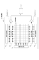
図1は、本発明に係る測距画素および撮像画素を有する撮像装置100のブロック図である。画素領域121と、垂直走査回路122と、2つの読み出し回路123と、2つの水平走査回路124と、2つの出力アンプ125を備えている。画素領域121以外の領域は周辺回路領域である。画素領域121には、多数の測距画素と撮像画素が2次元状に配列されている。周辺回路領域には、読み出し回路123、例えば、列アンプ、相関二重サンプリング(CDS)回路、加算回路等が設けられ、垂直走査回路122によって選択された行の画素から垂直信号線を介して読み出された信号に対して増幅、加算等を行う。水平走査回路124は、読み出し回路123から画素信号に基づく信号を順番に読み出すための信号を生成する。出力アンプ125は、水平走査回路124によって選択された列の信号を増幅して出力する。信号電荷として電子を用いる構成を例示するが、信号電荷として正孔を用いることも可能である。
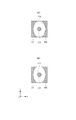
図2(A)は、測距画素800の断面図であり、図2(B)は測距画素800の平面図である。断面図で示した構成要素の一部を平面図では省略しており、断面図は平面図よりも抽象的に記載しているところもある。図2(A)において、符号810は、半導体基板、配線層、読み出し回路等を模式的に示した部材である。部材810の上には、下部電極となる電極801(第1の電極)と電極802(第2の電極)が設けられている。電極801と電極802の上には、光電変換層820と、上部電極となる対向電極830が設けられている。光電変換層820は、電極801(802)と対向電極830とに挟持されるように配されている。対向電極830の上には、カラーフィルタ840とマイクロレンズ850が設けられている。
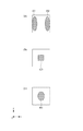
図4は、本実施形態の変形例を示したものである。図4(A)は、測距画素800の平面図である。本図に示すように、測距画素800の電極801、802は、矩形である必要はなく、楕円形であってもよい。また、図4(B)と(C)は、撮像画素900の平面図である。これらの図に示すように、撮像画素900の電極803は、矩形や楕円形であってもよい。また、電極803は五角形や八角形などの多角形であってもよい。
図5は、測距画素である第1の画素410と、第2の画素420の構成例を示したものである。第1の画素410には第1のマイクロレンズ(不図示)が設けられ、第2の画素420には第2のマイクロレンズ(不図示)が設けられている。実施形態1では、1つの測距画素は2つの電極を有していたが、図5に示すように、第1の画素410と、第2の画素420とに、それぞれ電極を1つ有する形態であってもよい。
図6(A)および(B)は、測距用の電極801と802、撮像用の電極803の全てを画素Pに配置した形態を示した断面図と平面図である。実施形態1および2では、測距画素と撮像画素とは別の画素であり、測距画素の中央部には、電極が設けられていなかった。しかし、本実施形態のように、測距用の構成と撮像用の構成を1つの画素に設けることも可能である。また、1つの画素に両方の構成を備えている場合において、図5(C)に示すように、撮像用の電極803の形状を踏襲するように、測距用の電極801と802が弧状に湾曲した形状を有していてもよい。
〈撮像システムの実施形態〉
本実施形態は、上記実施形態で説明した測距画素および撮像画素を含む撮像装置を用いた、撮像システムの実施形態である。撮像システムとしては、例えば車載カメラがある。
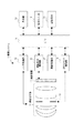
図12は、車載カメラに関する撮像システムの一例を示したものである。撮像システム1000は、本発明に係る測距画素および撮像画素を有する。撮像システム1000は、撮像装置1010により取得された複数の画像データに対し、画像処理を行う画像処理部1030と、撮像システム1000により取得された複数の画像データから視差(視差画像の位相差)の算出を行う視差算出部1040を有する。また、撮像システム1000は、算出された視差に基づいて対象物までの距離を算出する距離計測部1050と、算出された距離に基づいて衝突可能性があるか否かを判定する衝突判定部1060と、を有する。
801 第1の電極
802 第2の電極
803 第3の電極
900 撮像画素
Claims (10)
- 基板の上に2次元状に配列された複数の画素を有する撮像装置であって、
前記基板の上に設けられ、第1の電極と、第1の方向で前記第1の電極と対向して配されている第2の電極と、第3の電極とを有する画素電極と、
前記画素電極の上部に設けられた対向電極と、
前記画素電極と前記対向電極とで挟持されるように配された光電変換層と、を有し、
前記第1の方向において、前記第3の電極の幅は、前記第1の電極と前記第2の電極の間の距離よりも小さく、
前記第1の方向に直交する方向である第2の方向において、前記第3の電極の長さは、前記第1の電極の長さおよび前記第2の電極の長さよりも小さいことを特徴とする撮像装置。 - 前記第1の方向において、前記第1の電極および前記第2の電極の幅は、前記第3の電極の幅よりも小さいことを特徴とする請求項1に記載の撮像装置。
- 前記第1の電極と前記第2の電極に対応した共通のマイクロレンズが設けられていることを特徴とする請求項1または2に記載の撮像装置。
- 前記第1の電極に対応して設けられたマイクロレンズと、前記第2の電極に対応して設けられたマイクロレンズは、別のマイクロレンズであることを特徴とする請求項1または2に記載の撮像装置。
- 前記第1の電極と、前記第2の電極と、前記第3の電極とに対応した共通のマイクロレンズが設けられていることを特徴とする請求項3に記載の撮像装置。
- 前記第1の電極と前記第2の電極は矩形であり、前記第3の電極は円形であることを特徴とする請求項1から5のいずれかに記載の撮像装置。
- 前記第1の電極と前記第2の電極は弧状に湾曲した部分を有し、前記第3の電極は円形であることを特徴とする請求項1から5のいずれかに記載の撮像装置。
- 前記第3の電極の面積は、前記第1の電極の面積と前記第2の電極の面積の和よりも小さいことを特徴する請求項1から7のいずれかに記載の撮像装置。
- 半導体基板と、
第1の方向に沿って複数のマイクロレンズが配されることによって構成されたマイクロレンズ群が、前記第1の方向に直交する第2の方向に沿って複数配されたマイクロレンズアレイと、
前記マイクロレンズアレイと前記半導体基板との間に配された光電変換層を有する撮像装置であって、
前記半導体基板の上に設けられ、第1の電極と、前記第1の方向で前記第1の電極と対向して配されている第2の電極と、第3の電極とを有する画素電極と、
前記画素電極とともに前記光電変換層を挟持する対向電極とを有し、
前記マイクロレンズは、
第1の端部と、
前記第1の端部に対し、前記マイクロレンズの中心を挟んで前記第1の方向に配された第2の端部と、を有し、
前記第1の電極は前記第1の端部に重なるように配置され、
前記第2の電極は前記第2の端部に重なるように配置され、
前記第3の電極は前記マイクロレンズの中心に重なるように配置されており、
前記第1の方向において、前記第3の電極の幅は、前記第1の電極と前記第2の電極の間の距離よりも小さく、
前記第2の方向において、前記第3の電極の長さは、前記第1の電極の長さおよび前記第2の電極の長さよりも小さいことを特徴とする撮像装置。 - 移動体であって、
請求項1から9のいずれかに記載の撮像装置と、
前記撮像装置からの信号に基づく視差画像から、対象物までの距離情報を取得する距離情報取得手段と、
前記距離情報に基づいて前記移動体を制御する制御手段と、を有することを特徴とする移動体。
Priority Applications (2)
| Application Number | Priority Date | Filing Date | Title |
|---|---|---|---|
| JP2016042681A JP6789643B2 (ja) | 2016-03-04 | 2016-03-04 | 撮像装置 |
| US15/445,462 US10554915B2 (en) | 2016-03-04 | 2017-02-28 | Imaging sensor and moving body |
Applications Claiming Priority (1)
| Application Number | Priority Date | Filing Date | Title |
|---|---|---|---|
| JP2016042681A JP6789643B2 (ja) | 2016-03-04 | 2016-03-04 | 撮像装置 |
Publications (3)
| Publication Number | Publication Date |
|---|---|
| JP2017158159A true JP2017158159A (ja) | 2017-09-07 |
| JP2017158159A5 JP2017158159A5 (ja) | 2019-04-18 |
| JP6789643B2 JP6789643B2 (ja) | 2020-11-25 |
Family
ID=59722923
Family Applications (1)
| Application Number | Title | Priority Date | Filing Date |
|---|---|---|---|
| JP2016042681A Active JP6789643B2 (ja) | 2016-03-04 | 2016-03-04 | 撮像装置 |
Country Status (2)
| Country | Link |
|---|---|
| US (1) | US10554915B2 (ja) |
| JP (1) | JP6789643B2 (ja) |
Cited By (2)
| Publication number | Priority date | Publication date | Assignee | Title |
|---|---|---|---|---|
| JP2019133982A (ja) * | 2018-01-29 | 2019-08-08 | キヤノン株式会社 | 撮像装置、撮像システム及び移動体 |
| JP2020127179A (ja) * | 2019-02-06 | 2020-08-20 | キヤノン株式会社 | 画像処理装置 |
Families Citing this family (3)
| Publication number | Priority date | Publication date | Assignee | Title |
|---|---|---|---|---|
| JP6907029B2 (ja) | 2017-05-31 | 2021-07-21 | キヤノン株式会社 | 撮像装置 |
| JP7395300B2 (ja) * | 2019-03-22 | 2023-12-11 | キヤノン株式会社 | 光電変換装置、光電変換システム、および移動体 |
| CN111243331B (zh) * | 2019-04-23 | 2020-11-13 | 福州专志信息技术有限公司 | 现场信息识别反馈方法 |
Citations (4)
| Publication number | Priority date | Publication date | Assignee | Title |
|---|---|---|---|---|
| JP2007243744A (ja) * | 2006-03-10 | 2007-09-20 | Nikon Corp | 固体撮像素子及びこれを用いた電子カメラ |
| JP2014195296A (ja) * | 2009-04-07 | 2014-10-09 | Rohm Co Ltd | 画素回路およびそれを用いた光電変換装置 |
| JP2015207594A (ja) * | 2014-04-17 | 2015-11-19 | パナソニックIpマネジメント株式会社 | 固体撮像装置 |
| JP2015226255A (ja) * | 2014-05-29 | 2015-12-14 | 株式会社ニコン | 撮像装置および自動車 |
Family Cites Families (14)
| Publication number | Priority date | Publication date | Assignee | Title |
|---|---|---|---|---|
| JP2007158692A (ja) | 2005-12-05 | 2007-06-21 | Nikon Corp | 固体撮像素子及びこれを用いた電子カメラ |
| JP5283371B2 (ja) * | 2007-11-29 | 2013-09-04 | パナソニック株式会社 | 固体撮像素子 |
| EP2362257B1 (en) * | 2009-11-20 | 2016-08-17 | FUJIFILM Corporation | Solid-state imaging device |
| JP5742313B2 (ja) | 2011-03-10 | 2015-07-01 | 株式会社ニコン | 撮像装置 |
| US8742527B2 (en) * | 2011-09-27 | 2014-06-03 | Kabushiki Kaisha Toshiba | Solid state imaging device, solid state imaging element, portable information terminal device and method for manufacturing the solid state imaging element |
| JP2013172210A (ja) * | 2012-02-17 | 2013-09-02 | Canon Inc | 撮像装置 |
| JP2014067948A (ja) | 2012-09-27 | 2014-04-17 | Fujifilm Corp | 固体撮像素子および撮像装置 |
| WO2014097899A1 (ja) * | 2012-12-21 | 2014-06-26 | 富士フイルム株式会社 | 固体撮像装置 |
| WO2015046045A1 (ja) * | 2013-09-27 | 2015-04-02 | 富士フイルム株式会社 | 撮像装置及び撮像方法 |
| JP5946970B2 (ja) * | 2013-09-27 | 2016-07-06 | 富士フイルム株式会社 | 撮像装置及び撮像方法 |
| JP6682175B2 (ja) | 2014-07-31 | 2020-04-15 | キヤノン株式会社 | 固体撮像素子および撮像システム |
| JP2017054966A (ja) * | 2015-09-10 | 2017-03-16 | ルネサスエレクトロニクス株式会社 | 半導体装置の製造方法および半導体装置 |
| JP6706482B2 (ja) * | 2015-11-05 | 2020-06-10 | ソニーセミコンダクタソリューションズ株式会社 | 固体撮像装置および電子機器 |
| WO2017119477A1 (ja) * | 2016-01-08 | 2017-07-13 | 株式会社ニコン | 撮像素子および撮像装置 |
-
2016
- 2016-03-04 JP JP2016042681A patent/JP6789643B2/ja active Active
-
2017
- 2017-02-28 US US15/445,462 patent/US10554915B2/en active Active
Patent Citations (4)
| Publication number | Priority date | Publication date | Assignee | Title |
|---|---|---|---|---|
| JP2007243744A (ja) * | 2006-03-10 | 2007-09-20 | Nikon Corp | 固体撮像素子及びこれを用いた電子カメラ |
| JP2014195296A (ja) * | 2009-04-07 | 2014-10-09 | Rohm Co Ltd | 画素回路およびそれを用いた光電変換装置 |
| JP2015207594A (ja) * | 2014-04-17 | 2015-11-19 | パナソニックIpマネジメント株式会社 | 固体撮像装置 |
| JP2015226255A (ja) * | 2014-05-29 | 2015-12-14 | 株式会社ニコン | 撮像装置および自動車 |
Cited By (3)
| Publication number | Priority date | Publication date | Assignee | Title |
|---|---|---|---|---|
| JP2019133982A (ja) * | 2018-01-29 | 2019-08-08 | キヤノン株式会社 | 撮像装置、撮像システム及び移動体 |
| JP2020127179A (ja) * | 2019-02-06 | 2020-08-20 | キヤノン株式会社 | 画像処理装置 |
| JP7378935B2 (ja) | 2019-02-06 | 2023-11-14 | キヤノン株式会社 | 画像処理装置 |
Also Published As
| Publication number | Publication date |
|---|---|
| US10554915B2 (en) | 2020-02-04 |
| JP6789643B2 (ja) | 2020-11-25 |
| US20170257586A1 (en) | 2017-09-07 |
Similar Documents
| Publication | Publication Date | Title |
|---|---|---|
| JP6755679B2 (ja) | 撮像装置 | |
| CN108885099B (zh) | 能够获取图像并进行高精度测距的测距设备和移动物体 | |
| US10652496B2 (en) | Photoelectric conversion device, photoelectric conversion system, and movable body | |
| WO2017150553A1 (ja) | 撮像装置 | |
| JP6789643B2 (ja) | 撮像装置 | |
| JP2018077190A (ja) | 撮像装置及び自動制御システム | |
| JP7098790B2 (ja) | 撮像制御装置及び移動体 | |
| US10819931B2 (en) | Photoelectric conversion device, imaging system and mobile body | |
| US11417695B2 (en) | Photoelectric conversion apparatus, imaging system, and moving body | |
| US10708556B2 (en) | Imaging device and imaging system | |
| US11404456B2 (en) | Photoelectric conversion device | |
| JP7005331B2 (ja) | 撮像装置及び撮像システム | |
| US10798326B2 (en) | Imaging apparatus, signal processing apparatus, and moving body | |
| JP2019129375A (ja) | 撮像装置、撮像システム及び移動体 | |
| US11424283B2 (en) | Photoelectric conversion apparatus, imaging system and mobile body | |
| JP7305343B2 (ja) | 光電変換素子、光電変換素子の製造方法 | |
| JP2020170784A (ja) | 光電変換装置 |
Legal Events
| Date | Code | Title | Description |
|---|---|---|---|
| A521 | Request for written amendment filed |
Free format text: JAPANESE INTERMEDIATE CODE: A523 Effective date: 20160701 |
|
| A521 | Request for written amendment filed |
Free format text: JAPANESE INTERMEDIATE CODE: A821 Effective date: 20160705 |
|
| A521 | Request for written amendment filed |
Free format text: JAPANESE INTERMEDIATE CODE: A523 Effective date: 20190301 |
|
| A621 | Written request for application examination |
Free format text: JAPANESE INTERMEDIATE CODE: A621 Effective date: 20190301 |
|
| A977 | Report on retrieval |
Free format text: JAPANESE INTERMEDIATE CODE: A971007 Effective date: 20191127 |
|
| A131 | Notification of reasons for refusal |
Free format text: JAPANESE INTERMEDIATE CODE: A131 Effective date: 20191210 |
|
| A521 | Request for written amendment filed |
Free format text: JAPANESE INTERMEDIATE CODE: A523 Effective date: 20200207 |
|
| A131 | Notification of reasons for refusal |
Free format text: JAPANESE INTERMEDIATE CODE: A131 Effective date: 20200331 |
|
| A521 | Request for written amendment filed |
Free format text: JAPANESE INTERMEDIATE CODE: A523 Effective date: 20200509 |
|
| TRDD | Decision of grant or rejection written | ||
| A01 | Written decision to grant a patent or to grant a registration (utility model) |
Free format text: JAPANESE INTERMEDIATE CODE: A01 Effective date: 20201006 |
|
| A61 | First payment of annual fees (during grant procedure) |
Free format text: JAPANESE INTERMEDIATE CODE: A61 Effective date: 20201104 |
|
| R151 | Written notification of patent or utility model registration |
Ref document number: 6789643 Country of ref document: JP Free format text: JAPANESE INTERMEDIATE CODE: R151 |