JP2017162811A - 物体の構築方法およびそれに関連する粒子ビームシステム - Google Patents
物体の構築方法およびそれに関連する粒子ビームシステム Download PDFInfo
- Publication number
- JP2017162811A JP2017162811A JP2017043983A JP2017043983A JP2017162811A JP 2017162811 A JP2017162811 A JP 2017162811A JP 2017043983 A JP2017043983 A JP 2017043983A JP 2017043983 A JP2017043983 A JP 2017043983A JP 2017162811 A JP2017162811 A JP 2017162811A
- Authority
- JP
- Japan
- Prior art keywords
- particle beam
- substrate
- mark
- generated
- target structure
- Prior art date
- Legal status (The legal status is an assumption and is not a legal conclusion. Google has not performed a legal analysis and makes no representation as to the accuracy of the status listed.)
- Granted
Links
Images

Classifications
-
- H—ELECTRICITY
- H01—ELECTRIC ELEMENTS
- H01J—ELECTRIC DISCHARGE TUBES OR DISCHARGE LAMPS
- H01J37/00—Discharge tubes with provision for introducing objects or material to be exposed to the discharge, e.g. for the purpose of examination or processing thereof
- H01J37/30—Electron-beam or ion-beam tubes for localised treatment of objects
- H01J37/304—Controlling tubes by information coming from the objects or from the beam, e.g. correction signals
- H01J37/3045—Object or beam position registration
-
- H—ELECTRICITY
- H01—ELECTRIC ELEMENTS
- H01J—ELECTRIC DISCHARGE TUBES OR DISCHARGE LAMPS
- H01J37/00—Discharge tubes with provision for introducing objects or material to be exposed to the discharge, e.g. for the purpose of examination or processing thereof
- H01J37/26—Electron or ion microscopes; Electron or ion diffraction tubes
-
- H—ELECTRICITY
- H01—ELECTRIC ELEMENTS
- H01J—ELECTRIC DISCHARGE TUBES OR DISCHARGE LAMPS
- H01J37/00—Discharge tubes with provision for introducing objects or material to be exposed to the discharge, e.g. for the purpose of examination or processing thereof
- H01J37/26—Electron or ion microscopes; Electron or ion diffraction tubes
- H01J37/28—Electron or ion microscopes; Electron or ion diffraction tubes with scanning beams
-
- H—ELECTRICITY
- H01—ELECTRIC ELEMENTS
- H01J—ELECTRIC DISCHARGE TUBES OR DISCHARGE LAMPS
- H01J37/00—Discharge tubes with provision for introducing objects or material to be exposed to the discharge, e.g. for the purpose of examination or processing thereof
- H01J37/30—Electron-beam or ion-beam tubes for localised treatment of objects
- H01J37/317—Electron-beam or ion-beam tubes for localised treatment of objects for changing properties of the objects or for applying thin layers thereon, e.g. for ion implantation
- H01J37/3174—Particle-beam lithography, e.g. electron beam lithography
- H01J37/3177—Multi-beam, e.g. fly's eye, comb probe
-
- H—ELECTRICITY
- H01—ELECTRIC ELEMENTS
- H01J—ELECTRIC DISCHARGE TUBES OR DISCHARGE LAMPS
- H01J2237/00—Discharge tubes exposing object to beam, e.g. for analysis treatment, etching, imaging
- H01J2237/30—Electron or ion beam tubes for processing objects
- H01J2237/317—Processing objects on a microscale
- H01J2237/31732—Depositing thin layers on selected microareas
-
- H—ELECTRICITY
- H01—ELECTRIC ELEMENTS
- H01J—ELECTRIC DISCHARGE TUBES OR DISCHARGE LAMPS
- H01J2237/00—Discharge tubes exposing object to beam, e.g. for analysis treatment, etching, imaging
- H01J2237/30—Electron or ion beam tubes for processing objects
- H01J2237/317—Processing objects on a microscale
- H01J2237/3174—Etching microareas
- H01J2237/31745—Etching microareas for preparing specimen to be viewed in microscopes or analyzed in microanalysers
-
- H—ELECTRICITY
- H01—ELECTRIC ELEMENTS
- H01J—ELECTRIC DISCHARGE TUBES OR DISCHARGE LAMPS
- H01J2237/00—Discharge tubes exposing object to beam, e.g. for analysis treatment, etching, imaging
- H01J2237/30—Electron or ion beam tubes for processing objects
- H01J2237/317—Processing objects on a microscale
- H01J2237/31749—Focused ion beam
-
- H—ELECTRICITY
- H01—ELECTRIC ELEMENTS
- H01J—ELECTRIC DISCHARGE TUBES OR DISCHARGE LAMPS
- H01J2237/00—Discharge tubes exposing object to beam, e.g. for analysis treatment, etching, imaging
- H01J2237/30—Electron or ion beam tubes for processing objects
- H01J2237/317—Processing objects on a microscale
- H01J2237/3175—Lithography
- H01J2237/31793—Problems associated with lithography
- H01J2237/31798—Problems associated with lithography detecting pattern defects
Landscapes
- Chemical & Material Sciences (AREA)
- Analytical Chemistry (AREA)
- Sampling And Sample Adjustment (AREA)
- Physical Vapour Deposition (AREA)
- Electron Beam Exposure (AREA)
Abstract
Description
3 第二の粒子ビームコラム
7 第一の粒子ビームコラム
13 基板
15 表面
17 イオンビーム
19 第一の電子ビーム
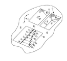
85 溝
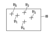
89 表面領域
91 マーク
Claims (12)
- 物体を構築する方法において、
基板を第一の粒子ビームコラムおよび第二の粒子ビームコラムの作業領域に配置するステップと、
前記第一の粒子ビームコラムにより生成された第一の粒子ビームを前記基板の複数の箇所に誘導して、そこに材料を堆積させるか、そこから材料を除去することによって、前記基板上に所望のターゲット構造を製造するステップと、
前記所望のターゲット構造の製造を繰り返し中断し、前記第一の粒子ビームを前記基板上に誘導することによって前記基板上にマークを生成し、前記所望のターゲット構造の製造を継続するステップと、
前記第二の粒子ビームコラムにより生成された第二の粒子ビームを前記基板上の前記マークへと誘導することによって前記基板上の前記マークの位置を捕捉し、前記プロセス中に前記基板上に前記第二の粒子ビームにより生成された粒子または放射を検出するステップと、
を含み、
前記第一の粒子ビームコラムにより生成される予定の前記第一の粒子ビームのビーム偏向は、前記捕捉されたマークの位置に依存して判断され、それによって前記第一の粒子ビームが前記基板の前記複数の箇所へと誘導される方法。 - 前記所望のターゲット構造は2つの表面領域を有し、その表面法線の向きには、5°より大きい、特に10°より大きい、特に15°より大きい差がある、請求項1に記載の方法。
- 前記所望のターゲット構造の製造を開始する前に、前記基板の上にマークを生成するステップをさらに含む、請求項1または2に記載の方法。
- 前記マークは前記基板の表面領域に隣接させて生成され、この表面領域の表面法線の向きには、5°未満、特に1°未満、および特に0.1°未満の差がある、請求項1〜3の何れか1項に記載の方法。
- 前記基板の表面領域に金属層を堆積させるステップをさらに含み、前記マークは前記金属層に生成される、請求項1〜4の何れか1項に記載の方法。
- 前記マークは各々、1本の直線または2本の交差する直線を含む、請求項1〜5の何れか1項に記載の方法。
- 前記第一の粒子ビーム装置の主軸と前記第二の粒子ビーム装置の主軸の相互に関して、10°より大きく、特に20°より大きく、特に30°より大きい角度で向き付けられる、請求項1〜6の何れか1項に記載の方法。
- 前記基板上の前記マークの位置を捕捉するステップは、少なくとも1対のマークの相互からの距離を測定するステップを含む、請求項1〜7の何れか1項に記載の方法。
- 前記第二の粒子ビームを前記基板の、前記ターゲット構造を製造している領域に誘導することによって、製造中の前記ターゲット構造の瞬間的形状を捕捉するステップと、前記プロセス中に前記第二の粒子ビームによって前記基板上に生成された粒子または放射を検出するステップと、をさらに含み、
前記第一の粒子ビームコラムによって生成される予定であり、前記第一の粒子ビームが前記基板上の複数の箇所に誘導されるような、前記第一の粒子ビームの前記ビーム偏向はさらに、製造中の前記ターゲット構造の前記捕捉された瞬間的形状に依存して判断される、
請求項1〜8の何れか1項に記載の方法。 - 前記第一の粒子ビームコラムにより生成される前記第一の粒子ビームはイオンビーム、特にガリウムイオンビームであり、前記第二の粒子ビームコラムにより生成される前記第二の粒子ビームは電子ビームである、請求項1〜9の何れか1項に記載の方法。
- 前記物体がTEMラメラである、請求項1〜10の何れか1項に記載の方法。
- 第一の粒子ビームコラムと、第二の粒子ビームコラムと、コントローラと、を含む粒子ビームシステムにおいて、
前記コントローラは、前記粒子ビームシステムを、それが請求項1〜11の何れか1項に記載の方法を実行するように制御するように構成された粒子ビームシステム。
Applications Claiming Priority (2)
| Application Number | Priority Date | Filing Date | Title |
|---|---|---|---|
| DE102016002883.1 | 2016-03-09 | ||
| DE102016002883.1A DE102016002883B4 (de) | 2016-03-09 | 2016-03-09 | Verfahren zum Struktuieren eines Objekts und Partikelstrahlsystem hierzu |
Publications (2)
| Publication Number | Publication Date |
|---|---|
| JP2017162811A true JP2017162811A (ja) | 2017-09-14 |
| JP6961367B2 JP6961367B2 (ja) | 2021-11-05 |
Family
ID=58455620
Family Applications (1)
| Application Number | Title | Priority Date | Filing Date |
|---|---|---|---|
| JP2017043983A Active JP6961367B2 (ja) | 2016-03-09 | 2017-03-08 | 物体の構築方法およびそれに関連する粒子ビームシステム |
Country Status (5)
| Country | Link |
|---|---|
| US (1) | US9960012B2 (ja) |
| JP (1) | JP6961367B2 (ja) |
| CZ (1) | CZ309996B6 (ja) |
| DE (1) | DE102016002883B4 (ja) |
| NL (1) | NL2018477B1 (ja) |
Families Citing this family (1)
| Publication number | Priority date | Publication date | Assignee | Title |
|---|---|---|---|---|
| DE102020134463B3 (de) | 2020-12-21 | 2022-06-23 | Carl Zeiss Microscopy Gmbh | Materialbearbeitungsverfahren und Materialbearbeitungssystem zur Ausführung des Verfahrens |
Citations (5)
| Publication number | Priority date | Publication date | Assignee | Title |
|---|---|---|---|---|
| JPH09274879A (ja) * | 1996-04-04 | 1997-10-21 | Hitachi Ltd | 集束イオンビーム装置の加工位置補正方法 |
| JP2009139379A (ja) * | 2007-12-06 | 2009-06-25 | Fei Co | デコレーションを用いたスライス・アンド・ビュー |
| JP2012022903A (ja) * | 2010-07-15 | 2012-02-02 | Hitachi High-Technologies Corp | 荷電粒子ビーム応用装置、および荷電粒子ビーム応用装置における基準マークの検出方法 |
| US20120112063A1 (en) * | 2009-03-26 | 2012-05-10 | Andreas Schertel | Method and apparatus for generating three-dimensional image data |
| US20140291512A1 (en) * | 2013-03-27 | 2014-10-02 | Hitachi High-Tech Science Corporation | Focused ion beam apparatus and method of working sample using the same |
Family Cites Families (7)
| Publication number | Priority date | Publication date | Assignee | Title |
|---|---|---|---|---|
| JPH01184824A (ja) | 1988-01-14 | 1989-07-24 | Oki Electric Ind Co Ltd | 位置合わせ方法 |
| DE10233002B4 (de) | 2002-07-19 | 2006-05-04 | Leo Elektronenmikroskopie Gmbh | Objektivlinse für ein Elektronenmikroskopiesystem und Elektronenmikroskopiesystem |
| JP5133737B2 (ja) | 2008-02-28 | 2013-01-30 | エスアイアイ・ナノテクノロジー株式会社 | 断面加工方法および装置 |
| US7880151B2 (en) | 2008-02-28 | 2011-02-01 | Fei Company | Beam positioning for beam processing |
| EP3528276A3 (en) * | 2011-05-13 | 2019-09-04 | Fibics Incorporated | Microscopy imaging method |
| CN104303257B (zh) | 2012-05-21 | 2018-03-30 | Fei 公司 | 用于tem观察的薄片的制备 |
| US8502172B1 (en) | 2012-06-26 | 2013-08-06 | Fei Company | Three dimensional fiducial |
-
2016
- 2016-03-09 DE DE102016002883.1A patent/DE102016002883B4/de active Active
-
2017
- 2017-03-02 CZ CZ2017-115A patent/CZ309996B6/cs unknown
- 2017-03-07 US US15/451,655 patent/US9960012B2/en active Active
- 2017-03-07 NL NL2018477A patent/NL2018477B1/nl not_active IP Right Cessation
- 2017-03-08 JP JP2017043983A patent/JP6961367B2/ja active Active
Patent Citations (7)
| Publication number | Priority date | Publication date | Assignee | Title |
|---|---|---|---|---|
| JPH09274879A (ja) * | 1996-04-04 | 1997-10-21 | Hitachi Ltd | 集束イオンビーム装置の加工位置補正方法 |
| JP2009139379A (ja) * | 2007-12-06 | 2009-06-25 | Fei Co | デコレーションを用いたスライス・アンド・ビュー |
| US20090242759A1 (en) * | 2007-12-06 | 2009-10-01 | Fei Company | Slice and view with decoration |
| US20120112063A1 (en) * | 2009-03-26 | 2012-05-10 | Andreas Schertel | Method and apparatus for generating three-dimensional image data |
| JP2012022903A (ja) * | 2010-07-15 | 2012-02-02 | Hitachi High-Technologies Corp | 荷電粒子ビーム応用装置、および荷電粒子ビーム応用装置における基準マークの検出方法 |
| US20140291512A1 (en) * | 2013-03-27 | 2014-10-02 | Hitachi High-Tech Science Corporation | Focused ion beam apparatus and method of working sample using the same |
| JP2014209450A (ja) * | 2013-03-27 | 2014-11-06 | 株式会社日立ハイテクサイエンス | 集束イオンビーム装置、それを用いた試料の加工方法、及び集束イオンビーム加工用コンピュータプログラム |
Also Published As
| Publication number | Publication date |
|---|---|
| US9960012B2 (en) | 2018-05-01 |
| CZ2017115A3 (cs) | 2017-10-18 |
| US20170263416A1 (en) | 2017-09-14 |
| CZ309996B6 (cs) | 2024-04-24 |
| DE102016002883A1 (de) | 2017-09-28 |
| DE102016002883B4 (de) | 2023-05-17 |
| JP6961367B2 (ja) | 2021-11-05 |
| NL2018477A (nl) | 2017-09-19 |
| NL2018477B1 (nl) | 2018-01-11 |
Similar Documents
| Publication | Publication Date | Title |
|---|---|---|
| JP5127148B2 (ja) | イオンビーム加工装置 | |
| KR101550921B1 (ko) | 단면 가공 방법 및 장치 | |
| JP5033314B2 (ja) | イオンビーム加工装置及び加工方法 | |
| US10340119B2 (en) | Automated TEM sample preparation | |
| US8796651B2 (en) | Method and apparatus for specimen fabrication | |
| JP6598684B2 (ja) | 荷電粒子ビームを用いた傾斜ミリングまたは視射角ミリング操作用の基準マーク設計 | |
| WO2016002341A1 (ja) | パターン測定方法、及びパターン測定装置 | |
| KR102047166B1 (ko) | 높이 측정 장치 및 하전 입자선 장치 | |
| JP6226781B2 (ja) | 集束イオンビーム装置、それを用いた試料の加工方法、及び集束イオンビーム加工用コンピュータプログラム | |
| JP5164355B2 (ja) | 荷電粒子ビームの走査方法及び荷電粒子線装置 | |
| JP6974820B2 (ja) | 荷電粒子ビーム装置、試料加工方法 | |
| US11532454B2 (en) | Imaging method and imaging system | |
| CN104245217A (zh) | 用于计算带电粒子束的射束参数的方法、测量设备及带电粒子束装置 | |
| JP6961367B2 (ja) | 物体の構築方法およびそれに関連する粒子ビームシステム | |
| JP5166315B2 (ja) | イオンビーム加工装置及び試料観察方法 | |
| JP5792767B2 (ja) | イオンビーム加工装置及び加工方法 | |
| KR102272157B1 (ko) | 하전 입자 빔 장치 | |
| JP2005135761A (ja) | Fibを用いた加工焦点位置修正方法とそれを実施する装置 | |
| JP2014239060A (ja) | 試料観察方法 | |
| JP5628862B2 (ja) | イオンビーム加工装置 |
Legal Events
| Date | Code | Title | Description |
|---|---|---|---|
| A621 | Written request for application examination |
Free format text: JAPANESE INTERMEDIATE CODE: A621 Effective date: 20200204 |
|
| A977 | Report on retrieval |
Free format text: JAPANESE INTERMEDIATE CODE: A971007 Effective date: 20210212 |
|
| A131 | Notification of reasons for refusal |
Free format text: JAPANESE INTERMEDIATE CODE: A131 Effective date: 20210302 |
|
| A521 | Request for written amendment filed |
Free format text: JAPANESE INTERMEDIATE CODE: A523 Effective date: 20210524 |
|
| TRDD | Decision of grant or rejection written | ||
| A01 | Written decision to grant a patent or to grant a registration (utility model) |
Free format text: JAPANESE INTERMEDIATE CODE: A01 Effective date: 20211005 |
|
| A61 | First payment of annual fees (during grant procedure) |
Free format text: JAPANESE INTERMEDIATE CODE: A61 Effective date: 20211013 |
|
| R150 | Certificate of patent or registration of utility model |
Ref document number: 6961367 Country of ref document: JP Free format text: JAPANESE INTERMEDIATE CODE: R150 |
|
| R250 | Receipt of annual fees |
Free format text: JAPANESE INTERMEDIATE CODE: R250 |
|
| R250 | Receipt of annual fees |
Free format text: JAPANESE INTERMEDIATE CODE: R250 |