JP2017163232A - Filter circuit, duplexer circuit, and front-end circuit - Google Patents
Filter circuit, duplexer circuit, and front-end circuit Download PDFInfo
- Publication number
- JP2017163232A JP2017163232A JP2016043920A JP2016043920A JP2017163232A JP 2017163232 A JP2017163232 A JP 2017163232A JP 2016043920 A JP2016043920 A JP 2016043920A JP 2016043920 A JP2016043920 A JP 2016043920A JP 2017163232 A JP2017163232 A JP 2017163232A
- Authority
- JP
- Japan
- Prior art keywords
- circuit
- filter
- impedance
- path
- terminal
- Prior art date
- Legal status (The legal status is an assumption and is not a legal conclusion. Google has not performed a legal analysis and makes no representation as to the accuracy of the status listed.)
- Pending
Links
- 230000008878 coupling Effects 0.000 claims abstract description 44
- 238000010168 coupling process Methods 0.000 claims abstract description 44
- 238000005859 coupling reaction Methods 0.000 claims abstract description 44
- 230000005540 biological transmission Effects 0.000 claims description 67
- 238000010586 diagram Methods 0.000 description 41
- 230000000052 comparative effect Effects 0.000 description 18
- 239000003990 capacitor Substances 0.000 description 10
- 230000004048 modification Effects 0.000 description 10
- 238000012986 modification Methods 0.000 description 10
- 238000004088 simulation Methods 0.000 description 10
- 238000004891 communication Methods 0.000 description 3
- 238000006243 chemical reaction Methods 0.000 description 2
- 238000004519 manufacturing process Methods 0.000 description 2
- 230000002776 aggregation Effects 0.000 description 1
- 238000004220 aggregation Methods 0.000 description 1
- 230000001419 dependent effect Effects 0.000 description 1
- 238000010295 mobile communication Methods 0.000 description 1
Images


Landscapes
- Transceivers (AREA)
- Transmitters (AREA)
Abstract
Description
本発明は、フィルタ回路、デュプレクサ回路およびフロントエンド回路であり、例えば、増幅回路の出力が入力されるフィルタを有するフィルタ回路、デュプレクサ回路およびフロントエンド回路である。 The present invention is a filter circuit, a duplexer circuit, and a front-end circuit, for example, a filter circuit, a duplexer circuit, and a front-end circuit having a filter to which an output of an amplifier circuit is input.
移動体通信の端末等の送信回路には、送信信号を増幅する増幅回路と、増幅された送信信号をフィルタリングするフィルタと、が用いられる。増幅回路の出力インピーダンスとフィルタの入力インピーダンスとが異なる場合、増幅回路とフィルタとの間にインピーダンス整合回路を設ける(特許文献1)。 An amplifier circuit that amplifies a transmission signal and a filter that filters the amplified transmission signal are used in a transmission circuit such as a mobile communication terminal. When the output impedance of the amplifier circuit and the input impedance of the filter are different, an impedance matching circuit is provided between the amplifier circuit and the filter (Patent Document 1).
しかしながら、フィルタの通過帯域において増幅回路の出力インピーダンスとフィルタの入力インピーダンスとを整合させても、通過帯域より周波数の高い所定の周波数ではインピーダンスが整合しない場合がある。このため、所定の周波数においてフィルタ特性が劣化することがある。 However, even if the output impedance of the amplifier circuit and the input impedance of the filter are matched in the pass band of the filter, the impedance may not match at a predetermined frequency higher than the pass band. For this reason, the filter characteristics may deteriorate at a predetermined frequency.
本発明は、上記課題に鑑みなされたものであり、通過帯域より高い周波数における特性を改善することを目的とする。 The present invention has been made in view of the above problems, and an object thereof is to improve characteristics at frequencies higher than the passband.
本発明は、入力端子を有するフィルタと、増幅回路と前記入力端子との間に接続され、前記フィルタの通過帯域において前記増幅回路の出力インピーダンスと前記入力端子の入力インピーダンスとを整合させる第1経路と、終端回路と前記入力端子との間に接続され、前記通過帯域より高い所定の周波数において前記終端回路の終端インピーダンスと前記入力端子の入力インピーダンスとを整合させる第2経路と、前記第1経路と前記第2経路とを結合し前記入力端子に接続する結合回路と、を具備するフィルタ回路である。 The present invention provides a filter having an input terminal, a first path connected between the amplifier circuit and the input terminal, and matching the output impedance of the amplifier circuit and the input impedance of the input terminal in the pass band of the filter. And a second path connected between the termination circuit and the input terminal and matching the termination impedance of the termination circuit and the input impedance of the input terminal at a predetermined frequency higher than the passband, and the first path And a coupling circuit that couples the second path and connects to the input terminal.
上記構成において、前記結合回路は、前記第1経路と前記入力端子との間に接続されたローパスフィルタと、前記第2経路と前記入力端子とに間に接続されたハイパスフィルタと、の少なくとも一方を有する構成とすることができる。 In the above configuration, the coupling circuit includes at least one of a low-pass filter connected between the first path and the input terminal, and a high-pass filter connected between the second path and the input terminal. It can be set as the structure which has these.
上記構成において、前記第1経路は、前記増幅回路と前記結合回路との間に接続され、前記フィルタの通過帯域において前記増幅回路の出力インピーダンスと前記入力端子の入力インピーダンスとを整合させる第1整合回路を有する構成とすることができる。 In the above-described configuration, the first path is connected between the amplifier circuit and the coupling circuit, and a first matching that matches an output impedance of the amplifier circuit and an input impedance of the input terminal in a pass band of the filter. A structure having a circuit can be employed.
上記構成において、前記第2経路は、前記終端回路と前記結合回路との間に接続され、前記所定の周波数において前記終端回路の終端インピーダンスと前記入力端子の入力インピーダンスとを整合させる第2整合回路を有する構成とすることができる。 In the above configuration, the second path is connected between the termination circuit and the coupling circuit, and matches the termination impedance of the termination circuit and the input impedance of the input terminal at the predetermined frequency. It can be set as the structure which has these.
本発明は、入力端子を有するフィルタと、増幅回路と前記入力端子との間に接続され、前記フィルタの通過帯域において前記増幅回路の出力インピーダンスと前記入力端子の入力インピーダンスとを整合させる第1経路と、前記増幅回路と前記入力端子との間に接続され、前記通過帯域より高い所定の周波数において前記増幅回路の出力インピーダンスと前記入力端子の入力インピーダンスとを整合させる第2経路と、前記増幅回路の出力を分岐し前記第1経路と前記第2経路とに接続する分岐回路と、前記第1経路と前記第2経路とを結合し前記入力端子に接続する結合回路と、を具備するフィルタ回路である。 The present invention provides a filter having an input terminal, a first path connected between the amplifier circuit and the input terminal, and matching the output impedance of the amplifier circuit and the input impedance of the input terminal in the pass band of the filter. And a second path connected between the amplifier circuit and the input terminal and matching the output impedance of the amplifier circuit and the input impedance of the input terminal at a predetermined frequency higher than the passband, and the amplifier circuit And a coupling circuit that couples the first path and the second path and connects the input path to the input terminal. It is.
上記構成において、前記分岐回路は、前記増幅回路と前記第1経路との間に接続されたローパスフィルタと、前記増幅回路と前記第2経路との間に接続されたハイパスフィルタと、の少なくとも一方を有し、前記結合回路は、前記第1経路と前記入力端子との間に接続されたローパスフィルタと、前記第2経路と前記入力端子との間に接続されたハイパスフィルタと、の少なくとも一方を有する構成とすることができる。 In the above configuration, the branch circuit includes at least one of a low-pass filter connected between the amplifier circuit and the first path, and a high-pass filter connected between the amplifier circuit and the second path. And the coupling circuit includes at least one of a low-pass filter connected between the first path and the input terminal, and a high-pass filter connected between the second path and the input terminal. It can be set as the structure which has these.
上記構成において、前記第1経路は、前記分岐回路と前記結合回路との間に接続され、前記フィルタの通過帯域において前記増幅回路の出力インピーダンスと前記入力端子の入力インピーダンスとを整合させる第1整合回路を有する構成とすることができる。 In the above-described configuration, the first path is connected between the branch circuit and the coupling circuit, and a first matching that matches an output impedance of the amplifier circuit and an input impedance of the input terminal in a pass band of the filter. A structure having a circuit can be employed.
上記構成において、前記第2経路は、前記分岐回路と前記結合回路との間に接続され、前記所定の周波数において前記増幅回路の出力インピーダンスと前記入力端子の入力インピーダンスとを整合させる第2整合回路を有する構成とすることができる。 In the above configuration, the second path is connected between the branch circuit and the coupling circuit, and matches the output impedance of the amplifier circuit and the input impedance of the input terminal at the predetermined frequency. It can be set as the structure which has these.
上記構成において、前記所定の周波数は前記通過帯域の高調波の周波数である構成とすることができる。 In the above configuration, the predetermined frequency may be a harmonic frequency of the passband.
本発明は、上記フィルタ回路であって、共通端子と送信端子との間に接続され、前記フィルタの出力端子が前記共通端子に接続されたフィルタ回路と、前記共通端子と受信端子との間に接続された受信フィルタと、を具備するデュプレクサ回路である。 The present invention is the above-described filter circuit, wherein the filter circuit is connected between a common terminal and a transmission terminal, and an output terminal of the filter is connected to the common terminal, and between the common terminal and the reception terminal. A duplexer circuit including a reception filter connected thereto;
本発明は、上記フィルタ回路であって、第1共通端子と第1送信端子との間に接続され前記フィルタの出力端子が前記第1共通端子に接続されたフィルタ回路と、前記第1共通端子と第2受信端子との間に接続された第1受信フィルタと、を有し、前記第1共通端子がアンテナに接続された第1デュプレクサと、前記アンテナに接続された第2共通端子と第2送信端子との間に接続された送信フィルタと、前記第2共通端子と第2受信端子との間に接続され前記高調波の周波数と重なる通過帯域を有する第2受信フィルタと、を有する第2デュプレクサと、を具備するフロントエンド回路である。 The present invention is the above filter circuit, wherein the filter circuit is connected between the first common terminal and the first transmission terminal, and the output terminal of the filter is connected to the first common terminal, and the first common terminal. A first reception filter connected between the first reception filter and the second reception terminal, wherein the first common terminal is connected to the antenna; the second common terminal connected to the antenna; A transmission filter connected between the second transmission terminal and a second reception filter connected between the second common terminal and the second reception terminal and having a passband overlapping the harmonic frequency. 2 is a front-end circuit including two duplexers.
本発明によれば、通過帯域より高い周波数における特性を改善することができる。 According to the present invention, characteristics at a frequency higher than the pass band can be improved.
まず、増幅回路の特性について説明する。増幅回路においては、主信号を増幅するときに、主信号の高調波(2倍波および3倍波等)が生成されやすい。また、増幅回路の出力インピーダンスは周波数依存性が大きい。 First, the characteristics of the amplifier circuit will be described. In the amplifier circuit, when the main signal is amplified, harmonics (second harmonic, third harmonic, etc.) of the main signal are likely to be generated. In addition, the output impedance of the amplifier circuit is highly frequency dependent.
図1(a)は、比較例1に係るフィルタ回路の回路図、図1(b)は、増幅回路の利得の周波数特性の例を示す図、図1(c)は、増幅回路の出力インピーダンスの例を示すスミスチャートである。図1(a)に示すように、フィルタ回路110は、整合回路14およびバンドパスフィルタ10を備えている。増幅回路12の出力がフィルタ回路110に入力する。増幅回路12の出力は整合回路14を介しフィルタ10の入力端子に接続されている。増幅回路12は、周波数f1の主信号を増幅する。整合回路14は増幅回路12の出力インピーダンスとフィルタ10の入力インピーダンスとを整合させる。フィルタ10は、主信号の周波数f1を通過帯域とし、増幅回路12が増幅した信号をフィルタリングする。増幅回路12としてLTEバンドB18の送信信号用の増幅回路とし、主信号の周波数f1を約820MHz、主信号の2倍波の周波数f2を約1640MHzとする。なおLTEバンドは、LTE規格(E−UTRA Operating Band)に対応する周波数帯である。
1A is a circuit diagram of a filter circuit according to Comparative Example 1, FIG. 1B is a diagram illustrating an example of gain frequency characteristics of the amplifier circuit, and FIG. 1C is an output impedance of the amplifier circuit. It is a Smith chart which shows the example of. As shown in FIG. 1A, the
図1(b)に示すように、周波数f1およびf2での利得はそれぞれ約13.2dBおよび−50dBである。図1(c)に示すように、周波数f1における出力インピーダンスは46.0+j7.9である。このときのVSWR(Voltage Standing Wave Ratio)は約1.2であり、出力インピーダンスはほぼ50Ωとなっている。一方、周波数f2における出力インピーダンスは1.7+j3.1であり、VSWRは約29.5である。このように周波数f2では出力インピーダンスが50Ωから大きくずれている。 As shown in FIG. 1B, the gains at frequencies f1 and f2 are about 13.2 dB and −50 dB, respectively. As shown in FIG. 1C, the output impedance at the frequency f1 is 46.0 + j7.9. At this time, the VSWR (Voltage Standing Wave Ratio) is about 1.2, and the output impedance is about 50Ω. On the other hand, the output impedance at the frequency f2 is 1.7 + j3.1, and the VSWR is about 29.5. Thus, the output impedance is greatly deviated from 50Ω at the frequency f2.
以上のように、増幅回路12の出力インピーダンスは、主信号を増幅する周波数帯域では、ほぼ基準インピーダンスとなるように設定されている。しかし、周波数の異なる例えば2倍波の周波数における増幅回路の出力インピーダンスは、基準インピーダンスとは異なる。一方、フィルタ10の入力インピーダンスは基準インピーダンス等の一定のインピーダンスであり、かつその周波数依存はほとんどないことを前提に設計されている。
As described above, the output impedance of the
そこで、通過帯域より高周波側において、フィルタ回路の入力端子に基準インピーダンスである50Ωと異なるインピーダンスが接続された場合のフィルタ10の減衰特性をシミュレーションした。
Therefore, the attenuation characteristics of the
図2(a)は、比較例1を用いたデュプレクサ回路の回路図、図2(b)は、シミュレーションに用いた送信インピーダンスを示すスミスチャートである。デュプレクサ回路112はLTEバンドB18用である。図2(a)に示すように、デュプレクサ20は、送信フィルタ20aおよび受信フィルタ20bを有している。送信フィルタ20aは共通端子Antと送信端子Txとの間に接続されている。受信フィルタ20bは共通端子Antと受信端子Rxとの間に接続されている。共通端子Antと送信フィルタ20aおよび受信フィルタ20bとの間に整合回路26が接続されている。送信端子Txと送信フィルタ20aとの間に整合回路24aが接続されている。受信端子Rxと受信フィルタ20bとの間に整合回路24bが接続されている。整合回路24a、24bおよび26は、インピーダンスを整合させる回路である。共通端子Antおよび受信端子Rxは、50Ωの終端抵抗Rで終端されている。送信端子Txにはインピーダンス素子28が接続されている。
FIG. 2A is a circuit diagram of a duplexer circuit using Comparative Example 1, and FIG. 2B is a Smith chart showing transmission impedance used in the simulation. The
図2(b)を参照し、インピーダンス素子28の送信インピーダンスZtxを50Ω(図2(b)の黒点に相当する)として送信フィルタ20の減衰特性をシミュレーションした。また、1.32GHz以上において、送信インピーダンスZtxのVSWRを30とし位相を変化させ(図2(b)のXに相当する)送信フィルタ20の減衰特性をシミュレーションした。
With reference to FIG. 2B, the attenuation characteristic of the
図3(a)は、送信フィルタにおける周波数に対する減衰量のシミュレーション結果を示す図、図3(b)は、周波数が1645MHzにおける位相に対する減衰量を示す図である。図3(a)を参照し、太線は送信インピーダンスZtxを50Ωのとしたとき(図2(b)の黒点に対応する)の減衰特性である。点線は送信インピーダンスZtxのVSWRを30とし位相を変えたとき(図2(b)のXに対応する)の減衰特性である。送信インピーダンスZtxの位相が回転すると送信フィルタ20aの減衰特性が変化する。図3(b)に示すように、送信インピーダンスZtxが50Ωのとき、位相が変化しても減衰量は一定である。VSWRが30のとき、位相によって減衰量が変化する。この例では位相が90°から130°において、減衰量が劣化する。
FIG. 3A is a diagram showing a simulation result of the attenuation amount with respect to the frequency in the transmission filter, and FIG. 3B is a diagram showing the attenuation amount with respect to the phase when the frequency is 1645 MHz. Referring to FIG. 3A, the thick line represents the attenuation characteristic when the transmission impedance Ztx is 50Ω (corresponding to the black dot in FIG. 2B). The dotted line represents the attenuation characteristic when the phase is changed with the VSWR of the transmission impedance Ztx being 30 (corresponding to X in FIG. 2B). When the phase of the transmission impedance Ztx rotates, the attenuation characteristic of the
このように、通過帯域の2倍波において、送信端子Txに送信信号を出力する増幅回路の出力インピーダンスが基準インピーダンスからずれていると、送信フィルタ20aに所望の減衰量が得られない可能性がある。例えば、インピーダンス整合されていれば増幅回路12および/またはフィルタ10の製造ばらつきにより位相が変化してもフィルタ10の減衰量はほとんど変わらない。ところが、図3(b)のように、インピーダンス整合されていないと、増幅回路12および/またはフィルタ10の製造ばらつきにより位相が変化するとフィルタ10の減衰量が大きく変動してしまう。このため、増幅回路12で生成された主信号の高調波(例えば2倍波および/または3倍波)がフィルタ10で十分に抑圧されない可能性がある。
Thus, in the second harmonic of the pass band, if the output impedance of the amplifier circuit that outputs the transmission signal to the transmission terminal Tx deviates from the reference impedance, there is a possibility that a desired attenuation amount cannot be obtained in the transmission filter 20a. is there. For example, if the impedance is matched, the attenuation of the
図4は、実施例1に係るフィルタ回路を示す回路図である。図4に示すように、フィルタ回路100は、分岐回路17、整合回路14aおよび14b、結合回路16およびフィルタ10を有する。増幅回路12とフィルタ10との間に分岐回路17、整合回路14aおよび14b、並びに結合回路16が接続されている。分岐回路17はダイプレクサであり、増幅回路12の出力を2つの経路18aと18bに分岐する。経路18aは低周波経路であり、経路18bは高周波経路である。経路18aに整合回路14aが設けられている。経路18bに整合回路14bが設けられている。結合回路16はダイプレクサであり、経路18aと18bとを結合し、フィルタ10の入力端子Inに接続する。
FIG. 4 is a circuit diagram illustrating the filter circuit according to the first embodiment. As illustrated in FIG. 4, the
増幅回路12の出力インピーダンスはフィルタ10の通過帯域において基準インピーダンス(例えば50Ω)であり、通過帯域より高周波側(例えば通過帯域の2倍波)において基準インピーダンスからずれている。分岐回路17は、通過帯域の主信号50aを経路18aに通過させ、経路18bには通過させない、また、分岐回路17は通過帯域の2倍波(すなわち主信号の2倍波)の信号50bを経路18bに通過させ、経路18aには通過させない。整合回路14aは,通過帯域において増幅回路12の出力インピーダンス(例えば50Ω)をフィルタ10の入力インピーダンスに整合させる。整合回路14bは通過帯域の2倍波の周波数において、増幅回路12の出力インピーダンス(例えば50Ω)をフィルタ10の入力インピーダンスに整合させる。結合回路16は、経路18aの通過帯域の信号と経路18bの2倍波の信号20bとを合成しフィルタ10の入力端子Inに出力する。結合回路16は、経路18aの通過帯域の主信号50aをフィルタ10に通過させ、経路18aの通過帯域の2倍波の信号をフィルタ10に通過させない。また、結合回路16は、経路18bの通過帯域の2倍波の信号50bをフィルタ10に通過させ、経路18bの通過帯域の主信号をフィルタ10に通過させない。フィルタ10は、通過帯域の信号を出力端子Outに出力する。
The output impedance of the
比較例1および実施例1についてシミュレーションを行なった。シミュレーションはLTEバンドB1用デュプレクサについて行なった。図5(a)は、比較例1におけるシミュレーションを行なったフィルタ回路の回路図、図5(b)は、比較例1の減衰特性を示す図である。 A simulation was performed for Comparative Example 1 and Example 1. The simulation was performed on a duplexer for LTE band B1. FIG. 5A is a circuit diagram of a filter circuit for which a simulation in Comparative Example 1 was performed, and FIG. 5B is a diagram illustrating an attenuation characteristic of Comparative Example 1.
図5(a)に示すように、整合回路24aは、送信端子Txとグランドとの間に接続されたインダクタL1である。整合回路24bは、受信端子Rxとグランドとの間に接続されたインダクタL2である。整合回路26は、共通端子Antとグランドとの間に接続されたインダクタL3である。その他の構成は、図2(a)と同じであり、説明を省略する。送信インピーダンスZtxは、3GHz以上において、図2(b)と同様にVSWRを30として位相を変化させた。シミュレーションした終端抵抗Rを50Ωとし、各インダクタL1からL3のインダクタンスを以下とした。
L1=4.3nH、L2=7.5nH、L3=3.3nH
As shown in FIG. 5A, the
L1 = 4.3nH, L2 = 7.5nH, L3 = 3.3nH
図5(b)に示すように、太実線は送信インピーダンスZtxが50Ωで一定としたときの減衰特性である。点線は送信インピーダンスZtxのVSWRを30として位相を変化させたときの減衰特性である。図3(b)と同様に、送信インピーダンスZtxのVSWRを30として位相を変化させると減衰特性がばらつく。通過帯域の2倍波に相当する周波数帯域60において減衰量がばらついている。
As shown in FIG. 5B, the thick solid line shows the attenuation characteristic when the transmission impedance Ztx is constant at 50Ω. The dotted line shows the attenuation characteristics when the phase is changed with VSWR of the transmission impedance Ztx being 30. Similarly to FIG. 3B, the attenuation characteristic varies when the phase is changed with the VSWR of the transmission impedance Ztx being 30. The amount of attenuation varies in the
図6は、実施例1におけるシミュレーションを行なったフィルタ回路の回路図である。図6に示すように、結合回路16は、ローパスフィルタ(LPF)16aおよびハイパスフィルタ(HPF)16bを備えている。分岐回路17はLPF17aおよびHPF17bを備えている。LPF16aは、経路18aに直列にインダクタL4が接続され、シャントにキャパシタC4が接続されている。HPF16bはキャパシタC5とインダクタL5とを有するT型回路である。LPF17aはインダクタL8とキャパシタC8とを有するT型回路である。HPF17bはキャパシタC9とインダクタL9とを有するT型回路である。整合回路14aは経路18aとグランドとの間に接続されたインダクタL6を有する。整合回路14bは経路18bに直列に接続されたインダクタL7と経路18bとグランドとの間に接続されたキャパシタC7を有する。その他の構成は図4および図5(a)と同じであり説明を省略する。
FIG. 6 is a circuit diagram of a filter circuit for which a simulation is performed in the first embodiment. As shown in FIG. 6, the
シミュレーションした終端抵抗Rを50Ωとし、各インダクタのインダクタンスおよび各キャパシタのキャパシタンスを以下とした。
インダクタンス
L2=L7.5nH、L3=3.3nH、L4=4.2nH、L5=2nH
L6=4.8nH、L7=5.6nH、L8=4.2nH、L9=2nH
キャパシタンス
C4=4.7pF、C5=0.8pF
C7=1.0pF、C8=1.9pF、C9=0.8pF
The simulated termination resistance R was 50Ω, and the inductance of each inductor and the capacitance of each capacitor were as follows.
Inductance L2 = L7.5nH, L3 = 3.3nH, L4 = 4.2nH, L5 = 2nH
L6 = 4.8 nH, L7 = 5.6 nH, L8 = 4.2 nH, L9 = 2 nH
Capacitance C4 = 4.7 pF, C5 = 0.8 pF
C7 = 1.0 pF, C8 = 1.9 pF, C9 = 0.8 pF
図7(a)は、実施例1の減衰特性を示す図、図7(b)は、実施例1および比較例1の周波数が3.9GHzにおける位相に対する減衰量を示す図である。図7(a)に示すように、通過帯域の2倍波に相当する周波数帯域60では、送信インピーダンスZtxのVSWRを30として位相を変化させて(点線)も、50Ω(太実線)のときより減衰量が大きくなっている。図7(b)に示すように、実施例1は、比較例1に比べ位相が変化しても減衰量が安定している。
FIG. 7A is a diagram illustrating the attenuation characteristics of Example 1, and FIG. 7B is a diagram illustrating the attenuation amount with respect to the phase when the frequency of Example 1 and Comparative Example 1 is 3.9 GHz. As shown in FIG. 7A, in the
実施例1において、2倍波の周波数f2において減衰量が安定する理由を説明する。図8(a)および図8(b)は、それぞれ比較例1および実施例1のインピーダンスを説明する図である。図8(a)および図8(b)の回路は、図1(a)および図4と同じフィルタ回路110および100であり、説明を省略する。
In the first embodiment, the reason why the attenuation is stabilized at the frequency f2 of the second harmonic will be described. FIGS. 8A and 8B are diagrams illustrating the impedances of Comparative Example 1 and Example 1, respectively. The circuits in FIG. 8A and FIG. 8B are the
図8(a)に示すように、矢印61aのように、主信号の周波数f1における増幅回路12の出力インピーダンスは50Ωである。矢印62aのように、整合回路14は増幅回路12の出力インピーダンスをフィルタ10の入力インピーダンスZfiに変換する。矢印61bのように2倍波の周波数f2における増幅回路12の出力インピーダンスはZtxである。矢印62bのように、整合回路14が変換した後のインピーダンスはフィルタ10の入力インピーダンスと異なる値となる。このように、比較例1においては、主信号においては、インピーダンス整合する(すなわち、増幅回路12の出力インピーダンスとフィルタ10の入力インピーダンスが共役となる)が、2倍波においてはインピーダンス整合しない。
As shown in FIG. 8A, as indicated by an
図8(b)に示すように、実施例1では、分岐回路17および結合回路16が増幅回路12の出力信号を経路18aと18bとに分岐する。周波数f1の主信号は主に経路18aを伝搬し、周波数f2の2倍波信号は主に経路18bを伝搬する。経路18aに整合回路14a、経路18bに整合回路13aおよび13bが設けられている。整合回路13aおよび13bは整合回路14bの機能を説明するために仮想的に図示している。
As shown in FIG. 8B, in the first embodiment, the
周波数f1における経路18aでは、矢印63aのように、分岐回路17を介した増幅回路12の出力インピーダンスは50Ωである。整合回路14aは、増幅回路12の出力インピーダンスをフィルタ10の入力インピーダンスZfiに変換する。よって、周波数f1においては増幅回路12とフィルタ10とはインピーダンス整合する。
In the
周波数f2における経路18bでは、矢印63bのように分岐回路17を介した増幅回路12の出力インピーダンスはZtxである。矢印64bのように整合回路13aはZtxを50Ωに変換する。さらに、矢印65bのように整合回路13bは50Ωをフィルタ10の入力インピーダンスZfiに変換する。これにより、周波数f2において増幅回路12とフィルタ10とがインピーダンス整合する。以上のように、実施例1では、主信号に加え2倍波においても増幅回路12とフィルタ10とがインピーダンス整合する。これにより、2倍波のフィルタ特性を改善できる。なお、以上の説明では、結合回路16によるインピーダンス変換を考慮していない。結合回路16によりインピーダンスが変換される場合、整合回路14aおよび14bは、増幅回路12の出力インピーダンスを結合回路16を介してフィルタ10を見た入力インピーダンスに整合させればよい。分岐回路17についても同様である。
In the
実施例1では、周波数f2としてフィルタ10の通過帯域の2倍波を例に説明したが、周波数f2は例えば通過帯域の3倍波でもよい。また周波数f2は通過帯域の任意の高調波の周波数でもよい。周波数f2は、通過帯域より周波数の高い任意の周波数でもよい。
In the first embodiment, the second frequency of the pass band of the
図9(a)から図11(c)は、実施例1の変形例に係るフィルタ回路の回路図である。図9(a)に示すように、LPF16aおよび17aはL−C−LのT型フィルタであり、HPF16bおよび17bは、C−L−CのT型フィルタでもよい。図9(b)に示すように、LPF16aおよび17aはL−CのL型フィルタであり、HPF16bおよび17bは、C−LのL型フィルタでもよい。図9(c)に示すように、LPF16aおよび17aはインダクタであり、HPF16bおよび17bは、キャパシタでもよい。
FIG. 9A to FIG. 11C are circuit diagrams of filter circuits according to modifications of the first embodiment. As shown in FIG. 9A, the
図10(a)に示すように、LPF16aおよび17a並びにHPF16bおよび17bはインダクタおよびキャパシタが各々複数個接続されたフィルタでもよい。図9(a)から図10(a)のように、LPF16aおよび17a並びにHPF16bおよび17bはインダクタおよびキャパシタを用い集中定数回路として任意に設計できる。LPF16aおよび17a並びにHPF16bおよび17bは伝送線路を用いた分布定数回路として設計してもよい。
As shown in FIG. 10A, the
図10(b)に示すように、分岐回路17および結合回路16は各々ダイプレクサ部品でもよい。図10(c)に示すように増幅回路12の出力インピーダンスとフィルタ10の入力インピーダンスとが整合している場合、整合回路14aは設けなくてもよい。
As shown in FIG. 10B, each of the
図11(a)に示すように、整合回路14bが主信号の周波数f1より高く、2倍波の周波数f2より低い遮断周波数を有するハイパスフィルタとして機能する場合、HPF16bおよび17bは設けなくてもよい。図11(b)に示すように、整合回路14aが主信号の周波数f1より高く2倍波の周波数f2より低い遮断周波数を有するローパスフィルタとして機能する場合、LPF16aおよび17aは設けなくてもよい。図11(c)に示すように、整合回路14bおよび14aがそれぞれ図11(a)および図11(b)と同様に機能する場合、LPF16aおよび17a並びにHPF16bおよび17bは設けなくてもよい。
As shown in FIG. 11A, when the
実施例1およびその変形例によれば、図4のように、経路18a(第1経路)は、増幅回路12と入力端子Inとの間に接続され、フィルタ10の通過帯域において増幅回路12の出力インピーダンスと入力端子Inの入力インピーダンスとを整合させる。経路18b(第2経路)は、増幅回路12と入力端子Inとの間に接続され、通過帯域より高い所定の周波数において増幅回路12の出力インピーダンスと入力端子Inの入力インピーダンスとを整合させる。分岐回路17は、増幅回路12の出力を分岐し経路18aと18bとに接続する。結合回路16は、経路18aと経路18bを結合し入力端子Inに接続する。これにより、経路18bにより、通過帯域より高い所定の周波数において増幅回路12とフィルタ10とのインピーダンスが整合される。このため、増幅回路12において生成された高調波等のフィルタ10の通過帯域より高い所定の周波数のフィルタ特性を向上させることができる。
According to the first embodiment and its modification, as shown in FIG. 4, the
また、図9(a)から図11(c)のように、分岐回路17は、増幅回路12と経路18aとの間に接続されたLPF17aと、増幅回路12と経路18bとの間に接続されたHPF17bと、の少なくとも一方を有している。結合回路16は、経路18aと入力端子Inとの間に接続されたLPF16aと、経路18bと入力端子Inとの間に接続されたHPF16bと、の少なくとも一方を有している。これにより、経路18aと18bとの周波数を分離することができる。
9A to 11C, the
図11(a)および図11(b)のように、整合回路14bがハイパスフィルタの機能を有することにより、HPF16bおよび17bを省略できる。整合回路14aがローパスフィルタの機能を有することによりLPF16aおよび17aを省略できる。これにより、フィルタ回路の小型化が可能となる。
As shown in FIGS. 11A and 11B, the
経路18aは、分岐回路17と結合回路16との間に接続され、フィルタ10の通過帯域において増幅回路12の出力インピーダンスと入力端子Inの入力インピーダンスとを整合させる整合回路14a(第1整合回路)を有する。これにより、通過帯域における増幅回路12の出力インピーダンスとフィルタ10の入力インピーダンスを整合させることができる。
The
経路18bは、分岐回路17と結合回路16との間に接続され、所定の周波数において増幅回路12の出力インピーダンスと入力端子Inの入力インピーダンスとを整合させる整合回路14b(第2整合回路)を有する。これにより、所定の周波数における増幅回路12の出力インピーダンスとフィルタ10の入力インピーダンスを整合させることができる。
The
増幅回路12は主信号の高調波を生成する。よって、所定の周波数はフィルタ10の通過帯域の高調波の周波数であることが好ましい。これにより、増幅回路12が生成した高調波を抑制できる。
The
図12(a)は、実施例2に係るフィルタ回路を示す回路図、図12(b)は、実施例2のインピーダンスを説明する図である。図12(a)に示すように、フィルタ回路102には、実施例1と比較し分岐回路17および経路18bが設けられていない。終端回路19と結合回路16との間に経路18cが設けられている。経路18cに整合回路14bが設けられている。
FIG. 12A is a circuit diagram illustrating a filter circuit according to the second embodiment, and FIG. 12B is a diagram illustrating the impedance of the second embodiment. As shown in FIG. 12A, the
図12(b)に示すように、経路18aに設けられた整合回路14aは、主信号の周波数f1において増幅回路12の出力インピーダンス(50Ω)をフィルタ10の入力インピーダンスZfiに変換する。矢印66のように、終端回路19は2倍波の周波数f2において経路18cを基準インピーダンス(例えば50Ω)に終端する。周波数f2において、整合回路14bは終端回路19のインピーダンス(50Ω)をフィルタ10の入力インピーダンスZfiに変換する。これにより、周波数f2において、フィルタ10には終端回路19のインピーダンスが見えることになる。よって、比較例1のような2倍波における減衰量の変動を抑制できる。
As shown in FIG. 12B, the
図13(a)から図14(c)は、実施例2の変形例に係るフィルタ回路の回路図である。図13(a)に示すように、LPF16aはL−C−LのT型フィルタであり、HPF16bは、C−L−CのT型フィルタでもよい。LPF16aおよびHPF16bはインダクタおよびキャパシタ等の集中定数回路または伝送線路等の分布定数回路を用い設定することができる。
FIGS. 13A to 14C are circuit diagrams of filter circuits according to modifications of the second embodiment. As shown in FIG. 13A, the
図13(b)に示すように、結合回路16はダイプレクサ部品でもよい。図13(c)に示すように、周波数f1において増幅回路12の出力インピーダンスとフィルタ10の入力インピーダンスとが整合している場合、整合回路14aを設けなくてもよい。周波数f2において終端回路19とフィルタ10とがインピーダンス整合している場合、整合回路14bを設けなくてもよい。整合回路14aおよび14bのいずれか一方を設け、他方を設けなくてもよい。
As shown in FIG. 13B, the
図14(a)に示すように、整合回路14bが主信号の周波数f1より高く、2倍波の周波数f2より低い遮断周波数を有するハイパスフィルタとして機能する場合、HPF16bは設けなくてもよい。図14(b)に示すように、整合回路14aが主信号の周波数f1より高く2倍波の周波数f2より低い遮断周波数を有するローパスフィルタとして機能する場合、LPF16aは設けなくてもよい。図14(c)に示すように、整合回路14bおよび14aがそれぞれ図14(a)および図14(b)と同様に機能する場合、LPF16aおよびHPF16bは設けなくてもよい。
As shown in FIG. 14A, when the
実施例2によれば、経路18aは、増幅回路12とフィルタ10の入力端子Inとの間に接続され、フィルタ10の通過帯域において増幅回路12の出力インピーダンスと入力端子Inの入力インピーダンスとを整合させ。経路18c(第2経路)は、終端回路19と入力端子Inとの間に接続され、通過帯域より高い所定の周波数において終端回路19の終端インピーダンスと入力端子Inの入力インピーダンスとを整合させる。結合回路16は、経路18aと経路18cを結合し入力端子Inに接続する。これにより、経路18cにより、通過帯域より高い所定の周波数において終端回路19とフィルタ10とのインピーダンスが整合される。このため、増幅回路12において生成された高調波等のフィルタ10の通過帯域より高い所定の周波数のフィルタ特性を向上させることができる。
According to the second embodiment, the
図15(a)から図15(f)は、ローパスフィルタとして機能する整合回路の例である。整合回路14aとして、図15(a)のようにL−C−LのT型フィルタ、図15(b)に示すようにC−L−Cのπ型フィルタ、図15(c)のように、C−LのL型フィルタ、図15(d)のように、L−CのL型フィルタ、図15(e)のように直列L、図15(f)のようにシャントCを用いることができる。
FIG. 15A to FIG. 15F are examples of matching circuits that function as a low-pass filter. As the
図16(a)から図16(f)は、ハイパスフィルタとして機能する整合回路の例である。整合回路14bとして、図16(a)のようにC−L−CのT型フィルタ、図16(b)に示すようにL−C−Lのπ型フィルタ、図16(c)のように、L−CのL型フィルタ、図16(d)のように、C−LのL型フィルタ、図16(e)のように直列C、図16(f)のようにシャントLを用いることができる。
FIG. 16A to FIG. 16F are examples of matching circuits that function as high-pass filters. As the
以上のように、整合回路14aおよび14bは、集中定数回路を用い任意に設計できる。また、整合回路14aおよび14bは、分布定数回路を用い任意に設計してもよい。
As described above, the matching
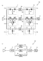
図17(a)および図17(b)は、実施例3に係るフィルタ回路の回路図である。図17(a)に示すように、フィルタ回路104において、分岐回路17は増幅回路12の出力を3つの経路18a、18bおよび18dに分岐する。結合回路16は、経路18a、18bおよび18dを結合する。分岐回路17および結合回路16は、経路18dに接続されたバンドパスフィルタ(BPF)17dおよび16dを有する。経路18a、18dおよび18bは、例えば主信号、主信号の2倍波および主信号の3倍波が伝搬する経路である。LPF16aおよび17aは主信号を通過させ、2倍波および3倍波を通過させない。BPF16dおよび17dは、2倍波を通過させ、主信号および3倍波を通過させない。HPF16bおよび17bは、3倍波を通過させ、主信号および2倍波を通過させない。
FIG. 17A and FIG. 17B are circuit diagrams of the filter circuit according to the third embodiment. As shown in FIG. 17A, in the
整合回路14aは、主信号における増幅回路12の出力インピーダンスをフィルタ10の入力インピーダンスに整合させる。整合回路14cは、2倍波における増幅回路12の出力インピーダンスをフィルタ10の入力インピーダンスに整合させる。整合回路14bは、3倍波における増幅回路12の出力インピーダンスをフィルタ10の入力インピーダンスに整合させる。これにより、2倍波および3倍波における減衰量の変動を抑制できる。
The matching
図17(b)に示すように、分岐回路17および結合回路16としてトリプレクサ部品を用いることができる。
As shown in FIG. 17B, triplexer parts can be used as the
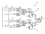
図18は、比較例2に係るフロントエンド回路を示す回路図である。図18に示すように、フロントエンド回路114は、ローバンド回路40とハイバンド回路42を有する。アンテナ38はダイプレクサ31を介しローバンド回路40およびハイバンド回路42のスイッチ30に接続される。ダイプレクサ31は、ローバンド回路40で用いる周波数のローバンド信号をローバンド回路40とアンテナ38との間で通過させ、ハイバンド回路42で用いる周波数のハイバンド信号をローバンド回路40とアンテナ38との間で通過させない。スイッチ30は複数のポートの1つを選択しアンテナ用ポートに接続する。スイッチ30の複数のポートは各々デュプレクサまたはフィルタ(不図示)が接続されている。
FIG. 18 is a circuit diagram illustrating a front-end circuit according to the second comparative example. As shown in FIG. 18, the
デュプレクサ20は、送信フィルタ20aおよび受信フィルタ20bを有している。送信フィルタ20aは共通端子と送信端子Txとの間に接続されている。受信フィルタ20bは共通端子と受信端子Rxとの間に接続されている。送信端子Txはパワーアンプ32の出力端子に接続されている。受信端子RxはIC(Integrated Circuit)36に接続されている。共通端子はスイッチ30、ダイプレクサ31を介しアンテナ38に接続されている。
The
ICのバンドB17またはB4の送信端子から出力された送信信号はパワーアンプ32で増幅される。パワーアンプ32から出力された信号は整合回路24aでインピーダンス変換されデュプレクサ20の送信フィルタ20aでフィルタリングされスイッチ30の1つのポートに出力する。スイッチ30がこのポートをアンテナ用ポートに接続すると、送信信号はダイプレクサ31を通過しアンテナ38から出力される。
The transmission signal output from the transmission terminal of the
アンテナ38に入力した受信信号はダイプレクサ31を通過しスイッチ30のアンテナ用ポートに至る。スイッチ30がデュプレクサ20の接続されたポートを選択すると、受信信号は受信フィルタ20bを通過し整合回路24bでインピーダンス変換されIC36のバンドB17またはB4の受信端子に至る。受信信号はIC36内のローノイズアンプで増幅される。
The received signal input to the
LTEバンドB17の送信帯域は704−716MHz、受信帯域は734−746MHzである。LTEバンドB4の送信帯域は1710−1755MHz、受信帯域は2110−2155MHzである。バンドB17の送信帯域の3倍波はバンドB4の受信帯域に重なっている。バンドB17用のパワーアンプ32に生成された3倍波が送信フィルタ20aで十分抑圧されないと、矢印70のように、バンドB4の受信フィルタ20bを通過してしまう。このように、バンドB17とB4のキャリアアグリゲーション動作において、バンドB17の送信をバンドB4の受信とを同時に行なおうとすると、バンドB17の送信信号の3倍波がバンドB4の妨害波となってしまう。
The transmission band of the LTE band B17 is 704 to 716 MHz, and the reception band is 734 to 746 MHz. The transmission band of the LTE band B4 is 1710-1755 MHz, and the reception band is 2110-2155 MHz. The third harmonic of the transmission band of band B17 overlaps with the reception band of band B4. If the third harmonic generated in the
図19は、実施例4に係るフロントエンド回路の回路図である。図19に示すように、フロントエンド回路106では、バンドB17の整合回路24aの代わりに、実施例2の整合回路14a、14b、結合回路16および終端回路19を用いる。整合回路14bは、バンドB17の送信信号の3倍波の周波数において、終端回路19のインピーダンスを送信フィルタ20aの入力インピーダンスに整合させる。これにより、バンドB17のパワーアンプ32が生成した送信信号の3倍波は結合回路16を通過しない。一方、送信信号の3倍波の周波数において送信フィルタ20aの入力は終端回路19のインピーダンスに終端されている。これにより、比較例2のように、バンドB17の送信信号の3倍波がバンドB4の受信信号の妨害波となることを抑制できる。
FIG. 19 is a circuit diagram of a front-end circuit according to the fourth embodiment. As shown in FIG. 19, in the
実施例4のように、デュプレクサ回路の送信フィルタ20aとして実施例1から3およびその変形例に係るフィルタ回路を用いることができる。これにより、パワーアンプ32から出力される高調波等の所定の周波数のフィルタ特性を改善することができる。
As in the fourth embodiment, the filter circuits according to the first to third embodiments and the modifications thereof can be used as the
ハイバンド回路42の受信フィルタ20bの通過帯域はローバンド回路40の送信フィルタ20aの通過帯域の高調波と重なる。このような構成のフロントエンド回路では、図18のように、ローバンド回路40の送信信号の高調波がハイバンド回路42の受信信号の妨害波となる。よって、ローバンド回路40の送信フィルタ20aとして実施例1から3およびその変形例のフィルタ回路を用いることが好ましい。これにより、ローバンド回路40の送信信号の高調波がハイバンド回路42の受信信号の妨害波となることを抑制できる。
The pass band of the
実施例5は、通信機器の例である。図20は、実施例5に係る通信機器の例である。図20に示すように、スマートフォン80と基地局82とは無線通信する。スマートフォン80等の移動端末および/または基地局等の固定端末に実施例1から4のフィルタ回路および/またはフロントエンド回路を用いることができる。
Example 5 is an example of a communication device. FIG. 20 is an example of a communication device according to the fifth embodiment. As shown in FIG. 20, the
以上、本発明の実施例について詳述したが、本発明はかかる特定の実施例に限定されるものではなく、特許請求の範囲に記載された本発明の要旨の範囲内において、種々の変形・変更が可能である。 Although the embodiments of the present invention have been described in detail above, the present invention is not limited to such specific embodiments, and various modifications and changes can be made within the scope of the gist of the present invention described in the claims. It can be changed.
10 フィルタ
12 増幅回路
14a、14b 整合回路
16 結合回路
17 分岐回路
18a−18d 経路
DESCRIPTION OF
Claims (11)
増幅回路と前記入力端子との間に接続され、前記フィルタの通過帯域において前記増幅回路の出力インピーダンスと前記入力端子の入力インピーダンスとを整合させる第1経路と、
終端回路と前記入力端子との間に接続され、前記通過帯域より高い所定の周波数において前記終端回路の終端インピーダンスと前記入力端子の入力インピーダンスとを整合させる第2経路と、
前記第1経路と前記第2経路とを結合し前記入力端子に接続する結合回路と、
を具備するフィルタ回路。 A filter having an input terminal;
A first path connected between an amplifier circuit and the input terminal and matching an output impedance of the amplifier circuit and an input impedance of the input terminal in a pass band of the filter;
A second path connected between the termination circuit and the input terminal and matching the termination impedance of the termination circuit and the input impedance of the input terminal at a predetermined frequency higher than the passband;
A coupling circuit coupling the first path and the second path and connecting to the input terminal;
A filter circuit comprising:
増幅回路と前記入力端子との間に接続され、前記フィルタの通過帯域において前記増幅回路の出力インピーダンスと前記入力端子の入力インピーダンスとを整合させる第1経路と、
前記増幅回路と前記入力端子との間に接続され、前記通過帯域より高い所定の周波数において前記増幅回路の出力インピーダンスと前記入力端子の入力インピーダンスとを整合させる第2経路と、
前記増幅回路の出力を分岐し前記第1経路と前記第2経路とに接続する分岐回路と、
前記第1経路と前記第2経路とを結合し前記入力端子に接続する結合回路と、
を具備するフィルタ回路。 A filter having an input terminal;
A first path connected between an amplifier circuit and the input terminal and matching an output impedance of the amplifier circuit and an input impedance of the input terminal in a pass band of the filter;
A second path connected between the amplifier circuit and the input terminal and matching the output impedance of the amplifier circuit and the input impedance of the input terminal at a predetermined frequency higher than the passband;
A branch circuit that branches the output of the amplifier circuit and connects the first path and the second path;
A coupling circuit coupling the first path and the second path and connecting to the input terminal;
A filter circuit comprising:
前記結合回路は、前記第1経路と前記入力端子との間に接続されたローパスフィルタと、前記第2経路と前記入力端子との間に接続されたハイパスフィルタと、の少なくとも一方を有する請求項5記載のフィルタ回路。 The branch circuit has at least one of a low-pass filter connected between the amplifier circuit and the first path, and a high-pass filter connected between the amplifier circuit and the second path,
The coupling circuit includes at least one of a low-pass filter connected between the first path and the input terminal and a high-pass filter connected between the second path and the input terminal. 6. The filter circuit according to 5.
前記共通端子と受信端子との間に接続された受信フィルタと、
を具備するデュプレクサ回路。 The filter circuit according to any one of claims 1 to 9, wherein the filter circuit is connected between a common terminal and a transmission terminal, and an output terminal of the filter is connected to the common terminal;
A reception filter connected between the common terminal and the reception terminal;
A duplexer circuit comprising:
前記アンテナに接続された第2共通端子と第2送信端子との間に接続された送信フィルタと、前記第2共通端子と第2受信端子との間に接続され前記高調波の周波数と重なる通過帯域を有する第2受信フィルタと、を有する第2デュプレクサと、
を具備するフロントエンド回路。 10. The filter circuit according to claim 9, wherein the filter circuit is connected between a first common terminal and a first transmission terminal, and an output terminal of the filter is connected to the first common terminal, and the first common terminal. A first receiving filter connected between the first receiving terminal and the second receiving terminal, wherein the first common terminal is connected to an antenna;
A transmission filter connected between a second common terminal connected to the antenna and a second transmission terminal, and a pass connected between the second common terminal and the second reception terminal and overlapping the harmonic frequency. A second duplexer having a second receive filter having a band;
A front-end circuit comprising:
Priority Applications (1)
| Application Number | Priority Date | Filing Date | Title |
|---|---|---|---|
| JP2016043920A JP2017163232A (en) | 2016-03-07 | 2016-03-07 | Filter circuit, duplexer circuit, and front-end circuit |
Applications Claiming Priority (1)
| Application Number | Priority Date | Filing Date | Title |
|---|---|---|---|
| JP2016043920A JP2017163232A (en) | 2016-03-07 | 2016-03-07 | Filter circuit, duplexer circuit, and front-end circuit |
Publications (1)
| Publication Number | Publication Date |
|---|---|
| JP2017163232A true JP2017163232A (en) | 2017-09-14 |
Family
ID=59857273
Family Applications (1)
| Application Number | Title | Priority Date | Filing Date |
|---|---|---|---|
| JP2016043920A Pending JP2017163232A (en) | 2016-03-07 | 2016-03-07 | Filter circuit, duplexer circuit, and front-end circuit |
Country Status (1)
| Country | Link |
|---|---|
| JP (1) | JP2017163232A (en) |
Cited By (2)
| Publication number | Priority date | Publication date | Assignee | Title |
|---|---|---|---|---|
| WO2020003640A1 (en) * | 2018-06-25 | 2020-01-02 | 株式会社村田製作所 | Front-end circuit |
| JPWO2022185504A1 (en) * | 2021-03-05 | 2022-09-09 |
-
2016
- 2016-03-07 JP JP2016043920A patent/JP2017163232A/en active Pending
Cited By (7)
| Publication number | Priority date | Publication date | Assignee | Title |
|---|---|---|---|---|
| WO2020003640A1 (en) * | 2018-06-25 | 2020-01-02 | 株式会社村田製作所 | Front-end circuit |
| CN112335182A (en) * | 2018-06-25 | 2021-02-05 | 株式会社村田制作所 | Front-end circuit |
| US11223377B2 (en) | 2018-06-25 | 2022-01-11 | Murata Manufacturing Co., Ltd. | Front-end circuit |
| CN112335182B (en) * | 2018-06-25 | 2022-02-08 | 株式会社村田制作所 | Front-end circuit |
| JPWO2022185504A1 (en) * | 2021-03-05 | 2022-09-09 | ||
| WO2022185504A1 (en) * | 2021-03-05 | 2022-09-09 | 三菱電機株式会社 | Multi-band filter |
| JP7286046B2 (en) | 2021-03-05 | 2023-06-02 | 三菱電機株式会社 | multiband filter |
Similar Documents
| Publication | Publication Date | Title |
|---|---|---|
| KR102041721B1 (en) | Composite filter apparatus, high-frequency front end circuit, and communication apparatus | |
| US9306535B2 (en) | Integrated receive filter including matched balun | |
| US11894621B2 (en) | Radio-frequency apparatus with multi-band balun with improved performance and associated methods | |
| CN107735955B (en) | High-frequency front-end circuit | |
| CN108432128B (en) | doherty amplifier | |
| US8909161B2 (en) | Transceiver front-end | |
| US10700659B2 (en) | Multiplexer, radio-frequency front end circuit, and communication terminal | |
| JP2009530939A (en) | Transmitter, power amplifier, and filtering method | |
| US11916514B2 (en) | Radio-frequency apparatus with multi-band wideband balun and associated methods | |
| WO2015002127A1 (en) | Power amplification module, and front end circuit | |
| KR102432604B1 (en) | Multiplexers, High-Frequency Front-End Circuits and Communication Devices | |
| JP2015061198A (en) | Electronic circuit | |
| KR101444551B1 (en) | Power amplifying circuit and front end module including the same | |
| US9960898B2 (en) | Radio frequency front-end circuit | |
| KR20130028656A (en) | Electronic component | |
| EP2870700B1 (en) | Transceiver front-end | |
| JP6822444B2 (en) | Composite filter device, high frequency front end circuit and communication device | |
| JP2017163232A (en) | Filter circuit, duplexer circuit, and front-end circuit | |
| JPWO2015053045A1 (en) | High frequency front end circuit | |
| CN106253876A (en) | Ladder type filter, duplexer and module | |
| EP2779470A1 (en) | Integrated circuit for transmitting and receiving an RF signal | |
| CN105580283A (en) | High frequency power amplifier, high frequency front end circuit, and wireless communication device | |
| US20160352365A1 (en) | High-frequency front end circuit | |
| WO2020202891A1 (en) | High-frequency module and communication device | |
| CN115735335B (en) | High-frequency modules and communication devices |