JP2017174889A - 被加工物の処理装置 - Google Patents
被加工物の処理装置 Download PDFInfo
- Publication number
- JP2017174889A JP2017174889A JP2016056940A JP2016056940A JP2017174889A JP 2017174889 A JP2017174889 A JP 2017174889A JP 2016056940 A JP2016056940 A JP 2016056940A JP 2016056940 A JP2016056940 A JP 2016056940A JP 2017174889 A JP2017174889 A JP 2017174889A
- Authority
- JP
- Japan
- Prior art keywords
- heat transfer
- heater
- valve
- electrostatic chuck
- pipe
- Prior art date
- Legal status (The legal status is an assumption and is not a legal conclusion. Google has not performed a legal analysis and makes no representation as to the accuracy of the status listed.)
- Granted
Links
Images


Classifications
-
- H—ELECTRICITY
- H10—SEMICONDUCTOR DEVICES; ELECTRIC SOLID-STATE DEVICES NOT OTHERWISE PROVIDED FOR
- H10P—GENERIC PROCESSES OR APPARATUS FOR THE MANUFACTURE OR TREATMENT OF DEVICES COVERED BY CLASS H10
- H10P72/00—Handling or holding of wafers, substrates or devices during manufacture or treatment thereof
- H10P72/04—Apparatus for manufacture or treatment
- H10P72/0431—Apparatus for thermal treatment
-
- H—ELECTRICITY
- H01—ELECTRIC ELEMENTS
- H01J—ELECTRIC DISCHARGE TUBES OR DISCHARGE LAMPS
- H01J37/00—Discharge tubes with provision for introducing objects or material to be exposed to the discharge, e.g. for the purpose of examination or processing thereof
- H01J37/32—Gas-filled discharge tubes
- H01J37/32431—Constructional details of the reactor
- H01J37/32697—Electrostatic control
-
- H—ELECTRICITY
- H10—SEMICONDUCTOR DEVICES; ELECTRIC SOLID-STATE DEVICES NOT OTHERWISE PROVIDED FOR
- H10P—GENERIC PROCESSES OR APPARATUS FOR THE MANUFACTURE OR TREATMENT OF DEVICES COVERED BY CLASS H10
- H10P72/00—Handling or holding of wafers, substrates or devices during manufacture or treatment thereof
- H10P72/70—Handling or holding of wafers, substrates or devices during manufacture or treatment thereof for supporting or gripping
- H10P72/72—Handling or holding of wafers, substrates or devices during manufacture or treatment thereof for supporting or gripping using electrostatic chucks
- H10P72/722—Details of electrostatic chucks
-
- H—ELECTRICITY
- H01—ELECTRIC ELEMENTS
- H01J—ELECTRIC DISCHARGE TUBES OR DISCHARGE LAMPS
- H01J37/00—Discharge tubes with provision for introducing objects or material to be exposed to the discharge, e.g. for the purpose of examination or processing thereof
- H01J37/32—Gas-filled discharge tubes
- H01J37/32009—Arrangements for generation of plasma specially adapted for examination or treatment of objects, e.g. plasma sources
- H01J37/32192—Microwave generated discharge
-
- H—ELECTRICITY
- H01—ELECTRIC ELEMENTS
- H01J—ELECTRIC DISCHARGE TUBES OR DISCHARGE LAMPS
- H01J37/00—Discharge tubes with provision for introducing objects or material to be exposed to the discharge, e.g. for the purpose of examination or processing thereof
- H01J37/32—Gas-filled discharge tubes
- H01J37/32431—Constructional details of the reactor
- H01J37/32715—Workpiece holder
- H01J37/32724—Temperature
-
- H—ELECTRICITY
- H10—SEMICONDUCTOR DEVICES; ELECTRIC SOLID-STATE DEVICES NOT OTHERWISE PROVIDED FOR
- H10P—GENERIC PROCESSES OR APPARATUS FOR THE MANUFACTURE OR TREATMENT OF DEVICES COVERED BY CLASS H10
- H10P72/00—Handling or holding of wafers, substrates or devices during manufacture or treatment thereof
- H10P72/04—Apparatus for manufacture or treatment
- H10P72/0431—Apparatus for thermal treatment
- H10P72/0432—Apparatus for thermal treatment mainly by conduction
-
- H—ELECTRICITY
- H10—SEMICONDUCTOR DEVICES; ELECTRIC SOLID-STATE DEVICES NOT OTHERWISE PROVIDED FOR
- H10P—GENERIC PROCESSES OR APPARATUS FOR THE MANUFACTURE OR TREATMENT OF DEVICES COVERED BY CLASS H10
- H10P72/00—Handling or holding of wafers, substrates or devices during manufacture or treatment thereof
- H10P72/04—Apparatus for manufacture or treatment
- H10P72/0431—Apparatus for thermal treatment
- H10P72/0434—Apparatus for thermal treatment mainly by convection
-
- H—ELECTRICITY
- H10—SEMICONDUCTOR DEVICES; ELECTRIC SOLID-STATE DEVICES NOT OTHERWISE PROVIDED FOR
- H10P—GENERIC PROCESSES OR APPARATUS FOR THE MANUFACTURE OR TREATMENT OF DEVICES COVERED BY CLASS H10
- H10P72/00—Handling or holding of wafers, substrates or devices during manufacture or treatment thereof
- H10P72/06—Apparatus for monitoring, sorting, marking, testing or measuring
- H10P72/0602—Temperature monitoring
-
- H—ELECTRICITY
- H10—SEMICONDUCTOR DEVICES; ELECTRIC SOLID-STATE DEVICES NOT OTHERWISE PROVIDED FOR
- H10P—GENERIC PROCESSES OR APPARATUS FOR THE MANUFACTURE OR TREATMENT OF DEVICES COVERED BY CLASS H10
- H10P72/00—Handling or holding of wafers, substrates or devices during manufacture or treatment thereof
- H10P72/70—Handling or holding of wafers, substrates or devices during manufacture or treatment thereof for supporting or gripping
- H10P72/72—Handling or holding of wafers, substrates or devices during manufacture or treatment thereof for supporting or gripping using electrostatic chucks
-
- H—ELECTRICITY
- H10—SEMICONDUCTOR DEVICES; ELECTRIC SOLID-STATE DEVICES NOT OTHERWISE PROVIDED FOR
- H10P—GENERIC PROCESSES OR APPARATUS FOR THE MANUFACTURE OR TREATMENT OF DEVICES COVERED BY CLASS H10
- H10P95/00—Generic processes or apparatus for manufacture or treatments not covered by the other groups of this subclass
- H10P95/90—Thermal treatments, e.g. annealing or sintering
-
- H—ELECTRICITY
- H01—ELECTRIC ELEMENTS
- H01J—ELECTRIC DISCHARGE TUBES OR DISCHARGE LAMPS
- H01J2237/00—Discharge tubes exposing object to beam, e.g. for analysis treatment, etching, imaging
- H01J2237/32—Processing objects by plasma generation
Landscapes
- Physics & Mathematics (AREA)
- Engineering & Computer Science (AREA)
- Plasma & Fusion (AREA)
- Chemical & Material Sciences (AREA)
- Analytical Chemistry (AREA)
- Container, Conveyance, Adherence, Positioning, Of Wafer (AREA)
- Drying Of Semiconductors (AREA)
Abstract
Description
Claims (11)
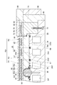
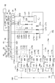
- 被加工物の処理装置であって、
チャンバ本体と、
前記チャンバ本体の内部に設けられた載置台と、
を備え、
前記載置台は、
冷媒用の流路が形成された金属製の冷却台と、
前記冷却台の上に設けられた静電チャックと、
を有し、
前記静電チャックは、該静電チャックの中心軸線に対して同心の複数の領域を含んでおり、該複数の領域にそれぞれ設けられた複数のヒータを有しており、
前記冷却台と前記静電チャックとの間、且つ、前記複数の領域それぞれの下方において延在し互いに分離された複数の伝熱空間が設けられており、
該処理装置は、
前記複数のヒータに接続されたヒータ電源と、
チラーユニット、伝熱ガスのガスソース、及び、排気装置を、前記複数の伝熱空間のそれぞれに選択的に接続し、前記チラーユニットと前記流路との接続と切断とを切り替えるための複数のバルブを有する配管系と、
を更に備える、
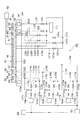
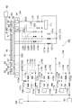
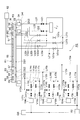
処理装置。 - 前記複数のバルブ及び前記ヒータ電源を制御する制御部を更に備え、
前記複数の領域は、第1領域、第2領域、及び、第3領域を含み、前記第1領域は、前記中心軸線に交差しており、前記第3領域は、前記静電チャックのエッジを含む領域であり、前記第2領域は、前記第1領域と前記第3領域との間にあり、
前記複数のヒータは、前記第1領域に設けられた第1のヒータ、前記第2領域に設けられた第2のヒータ、及び、前記第3領域に設けられた第3のヒータを含み、
前記複数の伝熱空間は、前記第1領域の下方にある第1の伝熱空間、前記第2領域の下方にある第2の伝熱空間、及び、前記第3領域の下方にある第3の伝熱空間を含む、
請求項1に記載の処理装置。 - 前記制御部は、前記複数のヒータに電力を供給するよう前記ヒータ電源を制御し、前記流路と前記チラーユニットとの間で冷媒を循環し、前記複数の伝熱空間を前記ガスソースに接続するよう前記複数のバルブを制御する、請求項2に記載の処理装置。
- 前記制御部は、前記第1のヒータの発熱量及び前記第2のヒータの発熱量が前記第3のヒータの発熱量よりも大きくなるよう前記ヒータ電源を制御し、前記流路と前記チラーユニットとの間で冷媒を循環し、前記第1の伝熱空間及び前記第2の伝熱空間を前記ガスソースに接続し、前記第3の伝熱空間を前記チラーユニットに接続するよう前記複数のバルブを制御する、請求項2又は3に記載の処理装置。
- 前記制御部は、前記第2のヒータの発熱量が前記第1のヒータの発熱量よりも大きくなり、前記第1のヒータの発熱量が前記第3のヒータの発熱量よりも大きくなるよう前記ヒータ電源を制御し、前記流路と前記チラーユニットとの間で冷媒を循環し、前記第1の伝熱空間及び前記第2の伝熱空間を前記ガスソースに接続し、前記第3の伝熱空間を前記チラーユニットに接続するよう前記複数のバルブを制御する、請求項2〜4の何れか一項に記載の処理装置。
- 前記制御部は、前記複数のヒータに電力を供給するよう前記ヒータ電源を制御し、前記複数の伝熱空間を前記チラーユニットに接続するよう前記複数のバルブを制御する、請求項2〜5の何れか一項に記載の処理装置。
- 前記制御部は、前記第1のヒータの発熱量及び前記第2のヒータの発熱量が前記第3のヒータの発熱量よりも大きくなるよう前記ヒータ電源を制御し、前記複数の伝熱空間を前記チラーユニットに接続するよう前記複数のバルブを制御する、請求項2〜6の何れか一項に記載の処理装置。
- 前記制御部は、前記複数のヒータに電力を供給するよう前記ヒータ電源を制御し、前記流路と前記チラーユニットとの間で冷媒を循環し、前記複数の伝熱空間を前記排気装置に接続するよう前記複数のバルブを制御する、請求項2〜7の何れか一項に記載の処理装置。
- 前記制御部は、前記複数のヒータへの電力の供給を停止するよう前記ヒータ電源を制御し、前記流路と前記チラーユニットとの間で冷媒を循環し、前記複数の伝熱空間を前記ガスソースに接続するよう前記複数のバルブを制御する、請求項2〜8の何れか一項に記載の処理装置。
- 前記制御部は、前記複数のヒータへの電力の供給を停止するよう前記ヒータ電源を制御し、前記流路と前記チラーユニットとの間で冷媒を循環し、前記複数の伝熱空間を前記チラーユニットに接続するよう前記複数のバルブを制御する、請求項2〜9の何れか一項に記載の処理装置。
- 前記静電チャックは、導電性の基台、及び、セラミックス製の吸着部を有し、
前記吸着部は、前記基台の上に設けられており、前記複数のヒータは、前記吸着部の中に内蔵されており、
該処理装置は、
前記基台に電気的に接続された高周波電源と、
前記チャンバ本体の内部に処理ガスを供給するガス供給部と、
を更に備える、
請求項1〜9の何れか一項に記載の処理装置。
Priority Applications (4)
| Application Number | Priority Date | Filing Date | Title |
|---|---|---|---|
| JP2016056940A JP6626753B2 (ja) | 2016-03-22 | 2016-03-22 | 被加工物の処理装置 |
| US15/459,028 US10665491B2 (en) | 2016-03-22 | 2017-03-15 | Processing apparatus for thermally processing a workpiece in a chamber |
| KR1020170033677A KR102325043B1 (ko) | 2016-03-22 | 2017-03-17 | 피가공물의 처리 장치 |
| TW106109309A TWI740914B (zh) | 2016-03-22 | 2017-03-21 | 被加工物之處理裝置 |
Applications Claiming Priority (1)
| Application Number | Priority Date | Filing Date | Title |
|---|---|---|---|
| JP2016056940A JP6626753B2 (ja) | 2016-03-22 | 2016-03-22 | 被加工物の処理装置 |
Publications (2)
| Publication Number | Publication Date |
|---|---|
| JP2017174889A true JP2017174889A (ja) | 2017-09-28 |
| JP6626753B2 JP6626753B2 (ja) | 2019-12-25 |
Family
ID=59898096
Family Applications (1)
| Application Number | Title | Priority Date | Filing Date |
|---|---|---|---|
| JP2016056940A Active JP6626753B2 (ja) | 2016-03-22 | 2016-03-22 | 被加工物の処理装置 |
Country Status (4)
| Country | Link |
|---|---|
| US (1) | US10665491B2 (ja) |
| JP (1) | JP6626753B2 (ja) |
| KR (1) | KR102325043B1 (ja) |
| TW (1) | TWI740914B (ja) |
Cited By (6)
| Publication number | Priority date | Publication date | Assignee | Title |
|---|---|---|---|---|
| WO2019155808A1 (ja) * | 2018-02-08 | 2019-08-15 | Sppテクノロジーズ株式会社 | 基板載置台及びこれを備えたプラズマ処理装置及びプラズマ処理方法 |
| WO2020054682A1 (ja) * | 2018-09-13 | 2020-03-19 | 日本碍子株式会社 | ウエハ載置装置 |
| KR20210091338A (ko) * | 2018-12-06 | 2021-07-21 | 도쿄엘렉트론가부시키가이샤 | 플라스마 처리 장치 및 플라스마 처리 방법 |
| JP2024524201A (ja) * | 2021-07-02 | 2024-07-05 | クァンウン ユニバーシティー インダストリーアカデミック コラボレーション ファウンデーション | マルチゾーン熱伝達構造物を用いた基板処理装置および温度制御方法 |
| WO2024209974A1 (ja) * | 2023-04-05 | 2024-10-10 | 東京エレクトロン株式会社 | 基板支持台及び基板処理装置 |
| WO2025204895A1 (ja) * | 2024-03-26 | 2025-10-02 | 東京エレクトロン株式会社 | 部材および部材の製造方法 |
Families Citing this family (15)
| Publication number | Priority date | Publication date | Assignee | Title |
|---|---|---|---|---|
| JP2018056333A (ja) * | 2016-09-29 | 2018-04-05 | 日本発條株式会社 | 基板載置台、および基板載置台の作製方法 |
| CN108987323B (zh) * | 2017-06-05 | 2020-03-31 | 北京北方华创微电子装备有限公司 | 一种承载装置及半导体加工设备 |
| KR102608397B1 (ko) * | 2018-10-16 | 2023-12-01 | 주식회사 미코세라믹스 | 미들 영역 독립 제어 세라믹 히터 |
| JP7101628B2 (ja) * | 2019-02-04 | 2022-07-15 | 東京エレクトロン株式会社 | プラズマ処理装置および電極構造体 |
| CN113130279B (zh) * | 2019-12-30 | 2023-09-29 | 中微半导体设备(上海)股份有限公司 | 下电极组件、等离子体处理装置及其工作方法 |
| US20230122167A1 (en) * | 2020-03-18 | 2023-04-20 | Lam Research Corporation | Method for conditioning a plasma processing chamber |
| KR102615216B1 (ko) * | 2020-05-15 | 2023-12-15 | 세메스 주식회사 | 정전 척, 기판 처리 장치 및 기판 처리 방법 |
| JP7515310B2 (ja) * | 2020-06-10 | 2024-07-12 | 東京エレクトロン株式会社 | 載置台、基板処理装置及び基板処理方法 |
| CN112002658B (zh) * | 2020-08-25 | 2024-06-21 | 北京北方华创微电子装备有限公司 | 加热器和加热基座 |
| JP7544450B2 (ja) * | 2021-03-17 | 2024-09-03 | 東京エレクトロン株式会社 | プラズマ処理装置 |
| US20220367236A1 (en) * | 2021-05-16 | 2022-11-17 | Applied Materials, Inc. | Heater pedestal with improved uniformity |
| KR102691521B1 (ko) * | 2021-10-15 | 2024-08-05 | 광운대학교 산학협력단 | 극저온 정전척 시스템 및 이의 제어 방법 |
| KR102800437B1 (ko) * | 2023-02-28 | 2025-04-23 | 광운대학교 산학협력단 | 고주파 급전 경로를 확보하기 위한 반도체 제조 시스템의 극저온 정전척 장치 |
| KR102903412B1 (ko) * | 2023-03-27 | 2025-12-24 | 토토 가부시키가이샤 | 정전 척 |
| WO2024206517A1 (en) * | 2023-03-31 | 2024-10-03 | Lam Research Corporation | Temperature-controlled pedestal for semiconductor wafer processing |
Citations (15)
| Publication number | Priority date | Publication date | Assignee | Title |
|---|---|---|---|---|
| JPH05243191A (ja) * | 1992-02-26 | 1993-09-21 | Nec Corp | ドライエッチング装置 |
| JPH0745523A (ja) * | 1993-07-27 | 1995-02-14 | Nec Corp | 減圧室の半導体基板加熱装置 |
| JP2002009064A (ja) * | 2000-06-21 | 2002-01-11 | Hitachi Ltd | 試料の処理装置及び試料の処理方法 |
| JP2002217178A (ja) * | 2001-01-23 | 2002-08-02 | Tokyo Electron Ltd | 処理装置及び処理方法 |
| JP2002327275A (ja) * | 2001-05-02 | 2002-11-15 | Tokyo Electron Ltd | 真空処理方法及び真空処理装置 |
| JP2002353298A (ja) * | 2001-05-23 | 2002-12-06 | Tokyo Electron Ltd | 載置装置 |
| JP2003249541A (ja) * | 2002-02-26 | 2003-09-05 | Hitachi High-Technologies Corp | ウエハステージ |
| JP2006261541A (ja) * | 2005-03-18 | 2006-09-28 | Tokyo Electron Ltd | 基板載置台、基板処理装置および基板処理方法 |
| JP2006526289A (ja) * | 2003-03-28 | 2006-11-16 | 東京エレクトロン株式会社 | 基板の温度コントロールのための方法とシステム |
| JP2007507104A (ja) * | 2003-09-26 | 2007-03-22 | 東京エレクトロン株式会社 | 連絡空間を用いた効率的な温度制御のための方法と装置 |
| JP2008177285A (ja) * | 2007-01-17 | 2008-07-31 | Hitachi High-Technologies Corp | プラズマ処理装置 |
| JP2008192643A (ja) * | 2007-01-31 | 2008-08-21 | Tokyo Electron Ltd | 基板処理装置 |
| JP2010123809A (ja) * | 2008-11-20 | 2010-06-03 | Tokyo Electron Ltd | 基板載置台および基板処理装置 |
| WO2013012025A1 (ja) * | 2011-07-20 | 2013-01-24 | 東京エレクトロン株式会社 | 載置台温度制御装置及び基板処理装置 |
| JP2014011382A (ja) * | 2012-07-02 | 2014-01-20 | Tokyo Electron Ltd | プラズマ処理装置、及び温度制御方法 |
Family Cites Families (6)
| Publication number | Priority date | Publication date | Assignee | Title |
|---|---|---|---|---|
| US5567267A (en) * | 1992-11-20 | 1996-10-22 | Tokyo Electron Limited | Method of controlling temperature of susceptor |
| JP5482282B2 (ja) | 2009-03-03 | 2014-05-07 | 東京エレクトロン株式会社 | 載置台構造及び成膜装置 |
| US9338871B2 (en) * | 2010-01-29 | 2016-05-10 | Applied Materials, Inc. | Feedforward temperature control for plasma processing apparatus |
| US10236194B2 (en) * | 2013-04-30 | 2019-03-19 | Semes Co., Ltd. | Supporting unit and substrate treatment apparatus |
| US20150060013A1 (en) * | 2013-09-05 | 2015-03-05 | Applied Materials, Inc. | Tunable temperature controlled electrostatic chuck assembly |
| KR20150090943A (ko) * | 2014-01-29 | 2015-08-07 | 세메스 주식회사 | 기판처리장치 및 방법 |
-
2016
- 2016-03-22 JP JP2016056940A patent/JP6626753B2/ja active Active
-
2017
- 2017-03-15 US US15/459,028 patent/US10665491B2/en active Active
- 2017-03-17 KR KR1020170033677A patent/KR102325043B1/ko active Active
- 2017-03-21 TW TW106109309A patent/TWI740914B/zh active
Patent Citations (15)
| Publication number | Priority date | Publication date | Assignee | Title |
|---|---|---|---|---|
| JPH05243191A (ja) * | 1992-02-26 | 1993-09-21 | Nec Corp | ドライエッチング装置 |
| JPH0745523A (ja) * | 1993-07-27 | 1995-02-14 | Nec Corp | 減圧室の半導体基板加熱装置 |
| JP2002009064A (ja) * | 2000-06-21 | 2002-01-11 | Hitachi Ltd | 試料の処理装置及び試料の処理方法 |
| JP2002217178A (ja) * | 2001-01-23 | 2002-08-02 | Tokyo Electron Ltd | 処理装置及び処理方法 |
| JP2002327275A (ja) * | 2001-05-02 | 2002-11-15 | Tokyo Electron Ltd | 真空処理方法及び真空処理装置 |
| JP2002353298A (ja) * | 2001-05-23 | 2002-12-06 | Tokyo Electron Ltd | 載置装置 |
| JP2003249541A (ja) * | 2002-02-26 | 2003-09-05 | Hitachi High-Technologies Corp | ウエハステージ |
| JP2006526289A (ja) * | 2003-03-28 | 2006-11-16 | 東京エレクトロン株式会社 | 基板の温度コントロールのための方法とシステム |
| JP2007507104A (ja) * | 2003-09-26 | 2007-03-22 | 東京エレクトロン株式会社 | 連絡空間を用いた効率的な温度制御のための方法と装置 |
| JP2006261541A (ja) * | 2005-03-18 | 2006-09-28 | Tokyo Electron Ltd | 基板載置台、基板処理装置および基板処理方法 |
| JP2008177285A (ja) * | 2007-01-17 | 2008-07-31 | Hitachi High-Technologies Corp | プラズマ処理装置 |
| JP2008192643A (ja) * | 2007-01-31 | 2008-08-21 | Tokyo Electron Ltd | 基板処理装置 |
| JP2010123809A (ja) * | 2008-11-20 | 2010-06-03 | Tokyo Electron Ltd | 基板載置台および基板処理装置 |
| WO2013012025A1 (ja) * | 2011-07-20 | 2013-01-24 | 東京エレクトロン株式会社 | 載置台温度制御装置及び基板処理装置 |
| JP2014011382A (ja) * | 2012-07-02 | 2014-01-20 | Tokyo Electron Ltd | プラズマ処理装置、及び温度制御方法 |
Cited By (16)
| Publication number | Priority date | Publication date | Assignee | Title |
|---|---|---|---|---|
| WO2019155808A1 (ja) * | 2018-02-08 | 2019-08-15 | Sppテクノロジーズ株式会社 | 基板載置台及びこれを備えたプラズマ処理装置及びプラズマ処理方法 |
| JP2019140211A (ja) * | 2018-02-08 | 2019-08-22 | Sppテクノロジーズ株式会社 | 基板載置台及びこれを備えたプラズマ処理装置及びプラズマ処理方法 |
| TWI812667B (zh) * | 2018-02-08 | 2023-08-21 | 日商Spp科技股份有限公司 | 基板載置台及具備該基板載置台的電漿處理裝置、以及電漿處理方法 |
| US11393664B2 (en) | 2018-02-08 | 2022-07-19 | Spp Technologies Co., Ltd. | Substrate placing table, plasma processing apparatus provided with same, and plasma processing method |
| KR20200110796A (ko) * | 2018-09-13 | 2020-09-25 | 엔지케이 인슐레이터 엘티디 | 웨이퍼 배치 장치 |
| JP6681522B1 (ja) * | 2018-09-13 | 2020-04-15 | 日本碍子株式会社 | ウエハ載置装置 |
| KR102423380B1 (ko) | 2018-09-13 | 2022-07-22 | 엔지케이 인슐레이터 엘티디 | 웨이퍼 배치 장치 |
| WO2020054682A1 (ja) * | 2018-09-13 | 2020-03-19 | 日本碍子株式会社 | ウエハ載置装置 |
| US11810767B2 (en) | 2018-09-13 | 2023-11-07 | Ngk Insulators, Ltd. | Wafer placement device |
| KR20210091338A (ko) * | 2018-12-06 | 2021-07-21 | 도쿄엘렉트론가부시키가이샤 | 플라스마 처리 장치 및 플라스마 처리 방법 |
| KR102604215B1 (ko) * | 2018-12-06 | 2023-11-21 | 도쿄엘렉트론가부시키가이샤 | 플라스마 처리 장치 및 플라스마 처리 방법 |
| US11990316B2 (en) | 2018-12-06 | 2024-05-21 | Tokyo Electron Limited | Plasma processing apparatus and plasma processing method |
| JP2024524201A (ja) * | 2021-07-02 | 2024-07-05 | クァンウン ユニバーシティー インダストリーアカデミック コラボレーション ファウンデーション | マルチゾーン熱伝達構造物を用いた基板処理装置および温度制御方法 |
| JP7671872B2 (ja) | 2021-07-02 | 2025-05-02 | クァンウン ユニバーシティー インダストリーアカデミック コラボレーション ファウンデーション | マルチゾーン熱伝達構造物を用いた基板処理装置および温度制御方法 |
| WO2024209974A1 (ja) * | 2023-04-05 | 2024-10-10 | 東京エレクトロン株式会社 | 基板支持台及び基板処理装置 |
| WO2025204895A1 (ja) * | 2024-03-26 | 2025-10-02 | 東京エレクトロン株式会社 | 部材および部材の製造方法 |
Also Published As
| Publication number | Publication date |
|---|---|
| TW201737408A (zh) | 2017-10-16 |
| KR20170110025A (ko) | 2017-10-10 |
| KR102325043B1 (ko) | 2021-11-11 |
| JP6626753B2 (ja) | 2019-12-25 |
| US10665491B2 (en) | 2020-05-26 |
| TWI740914B (zh) | 2021-10-01 |
| US20170278737A1 (en) | 2017-09-28 |
Similar Documents
| Publication | Publication Date | Title |
|---|---|---|
| JP6626753B2 (ja) | 被加工物の処理装置 | |
| CN107039326B (zh) | 载置台和等离子体处理装置 | |
| CN107833831B (zh) | 对氧化硅和氮化硅有选择地进行蚀刻的方法 | |
| US10515786B2 (en) | Mounting table and plasma processing apparatus | |
| JP6832171B2 (ja) | プラズマ処理装置のチャンバ本体の内部のクリーニングを含むプラズマ処理方法 | |
| JP6820206B2 (ja) | 被加工物を処理する方法 | |
| JP6982394B2 (ja) | 被加工物の処理装置、及び載置台 | |
| US12334305B2 (en) | Plasma processing apparatus | |
| JP2019029373A (ja) | 基板処理装置、及び、基板処理装置の運用方法 | |
| JP2018125461A (ja) | 被加工物の処理装置 | |
| JP7101055B2 (ja) | 静電チャック、フォーカスリング、支持台、プラズマ処理装置、及びプラズマ処理方法 |
Legal Events
| Date | Code | Title | Description |
|---|---|---|---|
| A621 | Written request for application examination |
Free format text: JAPANESE INTERMEDIATE CODE: A621 Effective date: 20180906 |
|
| A977 | Report on retrieval |
Free format text: JAPANESE INTERMEDIATE CODE: A971007 Effective date: 20190725 |
|
| A131 | Notification of reasons for refusal |
Free format text: JAPANESE INTERMEDIATE CODE: A131 Effective date: 20190813 |
|
| A521 | Request for written amendment filed |
Free format text: JAPANESE INTERMEDIATE CODE: A523 Effective date: 20191004 |
|
| TRDD | Decision of grant or rejection written | ||
| A01 | Written decision to grant a patent or to grant a registration (utility model) |
Free format text: JAPANESE INTERMEDIATE CODE: A01 Effective date: 20191105 |
|
| A61 | First payment of annual fees (during grant procedure) |
Free format text: JAPANESE INTERMEDIATE CODE: A61 Effective date: 20191202 |
|
| R150 | Certificate of patent or registration of utility model |
Ref document number: 6626753 Country of ref document: JP Free format text: JAPANESE INTERMEDIATE CODE: R150 |
|
| R250 | Receipt of annual fees |
Free format text: JAPANESE INTERMEDIATE CODE: R250 |
|
| R250 | Receipt of annual fees |
Free format text: JAPANESE INTERMEDIATE CODE: R250 |
|
| R250 | Receipt of annual fees |
Free format text: JAPANESE INTERMEDIATE CODE: R250 |
|
| R250 | Receipt of annual fees |
Free format text: JAPANESE INTERMEDIATE CODE: R250 |