JP2017181296A - 放射線検出器の製造方法 - Google Patents
放射線検出器の製造方法 Download PDFInfo
- Publication number
- JP2017181296A JP2017181296A JP2016068619A JP2016068619A JP2017181296A JP 2017181296 A JP2017181296 A JP 2017181296A JP 2016068619 A JP2016068619 A JP 2016068619A JP 2016068619 A JP2016068619 A JP 2016068619A JP 2017181296 A JP2017181296 A JP 2017181296A
- Authority
- JP
- Japan
- Prior art keywords
- resin frame
- frame
- resin
- scintillator layer
- radiation detector
- Prior art date
- Legal status (The legal status is an assumption and is not a legal conclusion. Google has not performed a legal analysis and makes no representation as to the accuracy of the status listed.)
- Granted
Links
Images





Classifications
-
- G—PHYSICS
- G01—MEASURING; TESTING
- G01T—MEASUREMENT OF NUCLEAR OR X-RADIATION
- G01T1/00—Measuring X-radiation, gamma radiation, corpuscular radiation, or cosmic radiation
- G01T1/16—Measuring radiation intensity
- G01T1/20—Measuring radiation intensity with scintillation detectors
-
- G—PHYSICS
- G01—MEASURING; TESTING
- G01T—MEASUREMENT OF NUCLEAR OR X-RADIATION
- G01T1/00—Measuring X-radiation, gamma radiation, corpuscular radiation, or cosmic radiation
- G01T1/16—Measuring radiation intensity
- G01T1/20—Measuring radiation intensity with scintillation detectors
- G01T1/2018—Scintillation-photodiode combinations
- G01T1/20187—Position of the scintillator with respect to the photodiode, e.g. photodiode surrounding the crystal, the crystal surrounding the photodiode, shape or size of the scintillator
-
- G—PHYSICS
- G01—MEASURING; TESTING
- G01T—MEASUREMENT OF NUCLEAR OR X-RADIATION
- G01T1/00—Measuring X-radiation, gamma radiation, corpuscular radiation, or cosmic radiation
- G01T1/16—Measuring radiation intensity
- G01T1/20—Measuring radiation intensity with scintillation detectors
- G01T1/2018—Scintillation-photodiode combinations
- G01T1/20188—Auxiliary details, e.g. casings or cooling
-
- G—PHYSICS
- G01—MEASURING; TESTING
- G01T—MEASUREMENT OF NUCLEAR OR X-RADIATION
- G01T1/00—Measuring X-radiation, gamma radiation, corpuscular radiation, or cosmic radiation
- G01T1/16—Measuring radiation intensity
- G01T1/20—Measuring radiation intensity with scintillation detectors
- G01T1/202—Measuring radiation intensity with scintillation detectors the detector being a crystal
-
- H—ELECTRICITY
- H10—SEMICONDUCTOR DEVICES; ELECTRIC SOLID-STATE DEVICES NOT OTHERWISE PROVIDED FOR
- H10F—INORGANIC SEMICONDUCTOR DEVICES SENSITIVE TO INFRARED RADIATION, LIGHT, ELECTROMAGNETIC RADIATION OF SHORTER WAVELENGTH OR CORPUSCULAR RADIATION
- H10F99/00—Subject matter not provided for in other groups of this subclass
Landscapes
- Physics & Mathematics (AREA)
- Health & Medical Sciences (AREA)
- Life Sciences & Earth Sciences (AREA)
- General Physics & Mathematics (AREA)
- High Energy & Nuclear Physics (AREA)
- Molecular Biology (AREA)
- Spectroscopy & Molecular Physics (AREA)
- Chemical & Material Sciences (AREA)
- Crystallography & Structural Chemistry (AREA)
- Measurement Of Radiation (AREA)
- Apparatus For Radiation Diagnosis (AREA)
- Electromagnetism (AREA)
Abstract
【解決手段】放射線検出器の製造方法は、複数の光電変換素子を含むセンサパネルの主面上に、複数の柱状結晶を含むシンチレータ層を気相堆積法によって形成する第1工程と、シンチレータ層を囲うように主面上に樹脂枠を形成すると共に、樹脂枠の外周に沿って樹脂枠に接するように無機固形材料からなる枠部材を配置する第2工程と、保護板を樹脂枠に接着することにより、シンチレータ層を封止する第3工程と、樹脂枠を硬化する第4工程と、を含む。
【選択図】図4
Description
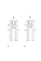
図10は、比較例に係る放射線検出器91を示す断面図である。この放射線検出器91は、センサパネル2、シンチレータ層3、中間層5、樹脂枠6及び保護板8を備えており、枠部材7を備えない点のみにおいて上記実施形態の放射線検出器1Aと相違している。本実施例では、枠部材7を有する放射線検出器1Aと枠部材7を有さない放射線検出器91とをサンプルとして、枠部材7の有無による防湿性能の違いについて試験した。試験では、温度を50℃、相対湿度を90%に調整した恒温槽内に各サンプルを配置し、X線特性(解像度、発光量)の推移を計測した。解像度の計測結果を表1に示す。また、発光量の計測結果を表2に示す。

Claims (7)
- 複数の光電変換素子を含むセンサパネルの主面上に、複数の柱状結晶を含むシンチレータ層を気相堆積法によって形成する第1工程と、
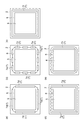
前記シンチレータ層を囲うように前記主面上に樹脂枠を形成すると共に、前記樹脂枠の外周に沿って前記樹脂枠に接するように無機固形材料からなる枠部材を配置する第2工程と、
保護板を前記樹脂枠に接着することにより、前記シンチレータ層を封止する第3工程と、
前記樹脂枠を硬化する第4工程と、を含む、放射線検出器の製造方法。 - 前記樹脂枠は、第1樹脂枠と第2樹脂枠とを含み、
前記第2工程では、前記シンチレータ層を囲うように前記第1樹脂枠を形成し、前記第1樹脂枠の外周に沿って前記第1樹脂枠に接するように前記枠部材を配置し、前記シンチレータ層を囲うように前記第1樹脂枠上に前記第2樹脂枠を形成する、請求項1に記載の放射線検出器の製造方法。 - 前記第2工程では、前記枠部材を配置した後であって、前記第2樹脂枠を形成する前に、前記第1樹脂枠を硬化する、請求項2に記載の放射線検出器の製造方法。
- 前記第1工程と前記第2工程との間に、中間層によって前記シンチレータ層の表面及び側面を被覆する第5工程をさらに含む、請求項1〜3のいずれか一項に記載の放射線検出器の製造方法。
- 前記第2工程では、前記中間層と接するように前記樹脂枠を形成する、請求項4に記載の放射線検出器の製造方法。
- 前記樹脂枠は紫外線硬化樹脂を含む、請求項1〜5のいずれか一項に記載の放射線検出器の製造方法。
- 前記枠部材はガラスロッドである、請求項1〜6のいずれか一項に記載の放射線検出器の製造方法。
Priority Applications (7)
| Application Number | Priority Date | Filing Date | Title |
|---|---|---|---|
| JP2016068619A JP6725288B2 (ja) | 2016-03-30 | 2016-03-30 | 放射線検出器の製造方法 |
| EP17773597.4A EP3438704B1 (en) | 2016-03-30 | 2017-01-26 | Radiation detector manufacturing method |
| PCT/JP2017/002748 WO2017169048A1 (ja) | 2016-03-30 | 2017-01-26 | 放射線検出器の製造方法 |
| KR1020187023921A KR20180124028A (ko) | 2016-03-30 | 2017-01-26 | 방사선 검출기의 제조 방법 |
| US16/088,481 US10983225B2 (en) | 2016-03-30 | 2017-01-26 | Radiation detector manufacturing method |
| CN201780019885.1A CN108885274A (zh) | 2016-03-30 | 2017-01-26 | 放射线检测器的制造方法 |
| TW106104486A TWI708958B (zh) | 2016-03-30 | 2017-02-10 | 放射線檢測器之製造方法 |
Applications Claiming Priority (1)
| Application Number | Priority Date | Filing Date | Title |
|---|---|---|---|
| JP2016068619A JP6725288B2 (ja) | 2016-03-30 | 2016-03-30 | 放射線検出器の製造方法 |
Publications (2)
| Publication Number | Publication Date |
|---|---|
| JP2017181296A true JP2017181296A (ja) | 2017-10-05 |
| JP6725288B2 JP6725288B2 (ja) | 2020-07-15 |
Family
ID=59962781
Family Applications (1)
| Application Number | Title | Priority Date | Filing Date |
|---|---|---|---|
| JP2016068619A Active JP6725288B2 (ja) | 2016-03-30 | 2016-03-30 | 放射線検出器の製造方法 |
Country Status (7)
| Country | Link |
|---|---|
| US (1) | US10983225B2 (ja) |
| EP (1) | EP3438704B1 (ja) |
| JP (1) | JP6725288B2 (ja) |
| KR (1) | KR20180124028A (ja) |
| CN (1) | CN108885274A (ja) |
| TW (1) | TWI708958B (ja) |
| WO (1) | WO2017169048A1 (ja) |
Cited By (1)
| Publication number | Priority date | Publication date | Assignee | Title |
|---|---|---|---|---|
| US11513240B2 (en) | 2018-11-13 | 2022-11-29 | Canon Electron Tubes & Devices Co., Ltd. | Radiation detection module, radiation detector, and method for manufacturing radiation detection module |
Families Citing this family (3)
| Publication number | Priority date | Publication date | Assignee | Title |
|---|---|---|---|---|
| JP7199332B2 (ja) | 2019-10-07 | 2023-01-05 | キヤノン電子管デバイス株式会社 | 放射線検出モジュールの製造方法 |
| JP7490951B2 (ja) * | 2019-12-13 | 2024-05-28 | コニカミノルタ株式会社 | 放射線検出パネル及び放射線画像検出器 |
| CN112540395A (zh) * | 2020-12-04 | 2021-03-23 | 清远先导材料有限公司 | 闪烁晶体阵列及其组装方法和拆卸方法 |
Citations (7)
| Publication number | Priority date | Publication date | Assignee | Title |
|---|---|---|---|---|
| JPH02296200A (ja) * | 1989-05-09 | 1990-12-06 | Konica Corp | 放射線画像変換パネル |
| WO2001051951A1 (fr) * | 2000-01-13 | 2001-07-19 | Hamamatsu Photonics K.K. | Capteur d'image radiologique et panneau de scintillateur |
| US20030001100A1 (en) * | 2001-06-29 | 2003-01-02 | Dejule Michael Clement | Cover plate having spacer lip with hermetic barrier for radiation imager and method of manufacturing same |
| JP2003262676A (ja) * | 2001-12-06 | 2003-09-19 | General Electric Co <Ge> | ディジタルX線検出器アセンブリの寿命を改善する直接式CsIシンチレータ・コーティング |
| WO2011108156A1 (ja) * | 2010-03-02 | 2011-09-09 | コニカミノルタエムジー株式会社 | 放射線検出パネル、放射線画像検出器、放射線検出パネルの製造方法および放射線画像検出器の製造方法 |
| JP2012185123A (ja) * | 2011-03-08 | 2012-09-27 | Sony Corp | 放射線撮像装置および放射線撮像装置の製造方法 |
| JP2015232503A (ja) * | 2014-06-10 | 2015-12-24 | 株式会社東芝 | 放射線検出器及びその製造方法 |
Family Cites Families (14)
| Publication number | Priority date | Publication date | Assignee | Title |
|---|---|---|---|---|
| CN1133881C (zh) | 1997-02-14 | 2004-01-07 | 浜松光子学株式会社 | 放射线检测元件及其制造方法 |
| CN1869732B (zh) * | 2000-01-13 | 2010-11-17 | 浜松光子学株式会社 | 放射线图像传感器及闪烁器板 |
| US6642524B2 (en) * | 2002-01-09 | 2003-11-04 | Ge Medical Systems Global Technology Company, Llc | Scintillator sealing for solid state X-ray detector |
| JP2004335580A (ja) | 2003-05-01 | 2004-11-25 | Canon Inc | 放射線撮像装置の製造方法 |
| US7067817B2 (en) * | 2004-01-29 | 2006-06-27 | Hamamatsu Photonics K.K. | Radiation image sensor and making method of same |
| US20080311484A1 (en) * | 2007-06-15 | 2008-12-18 | Hamamatsu Photonicfs K.K. | Radiation image conversion panel, scintillator panel, and radiation image sensor |
| JP4764407B2 (ja) | 2007-11-20 | 2011-09-07 | 東芝電子管デバイス株式会社 | 放射線検出器及びその製造方法 |
| JP2010243188A (ja) | 2009-04-01 | 2010-10-28 | Konica Minolta Medical & Graphic Inc | 放射線検出パネル、放射線画像検出器、放射線検出パネルの製造方法および放射線画像検出器の製造方法 |
| JP2011174830A (ja) * | 2010-02-25 | 2011-09-08 | Konica Minolta Medical & Graphic Inc | 放射線検出パネルおよび放射線画像検出器 |
| US8604440B2 (en) * | 2010-03-09 | 2013-12-10 | The University Of Chicago | Use of flat panel microchannel photomultipliers in sampling calorimeters with timing |
| JP5178900B2 (ja) | 2010-11-08 | 2013-04-10 | 富士フイルム株式会社 | 放射線検出器 |
| JP5728250B2 (ja) | 2011-03-01 | 2015-06-03 | キヤノン株式会社 | 放射線検出装置、シンチレータパネル、それらの製造方法、および放射線検出システム |
| JP6092568B2 (ja) * | 2012-10-11 | 2017-03-08 | キヤノン株式会社 | 放射線検出装置及び放射線検出システム |
| JP6523620B2 (ja) * | 2014-06-16 | 2019-06-05 | キヤノン電子管デバイス株式会社 | 放射線検出器及びその製造方法 |
-
2016
- 2016-03-30 JP JP2016068619A patent/JP6725288B2/ja active Active
-
2017
- 2017-01-26 EP EP17773597.4A patent/EP3438704B1/en active Active
- 2017-01-26 KR KR1020187023921A patent/KR20180124028A/ko not_active Ceased
- 2017-01-26 WO PCT/JP2017/002748 patent/WO2017169048A1/ja not_active Ceased
- 2017-01-26 CN CN201780019885.1A patent/CN108885274A/zh active Pending
- 2017-01-26 US US16/088,481 patent/US10983225B2/en active Active
- 2017-02-10 TW TW106104486A patent/TWI708958B/zh active
Patent Citations (7)
| Publication number | Priority date | Publication date | Assignee | Title |
|---|---|---|---|---|
| JPH02296200A (ja) * | 1989-05-09 | 1990-12-06 | Konica Corp | 放射線画像変換パネル |
| WO2001051951A1 (fr) * | 2000-01-13 | 2001-07-19 | Hamamatsu Photonics K.K. | Capteur d'image radiologique et panneau de scintillateur |
| US20030001100A1 (en) * | 2001-06-29 | 2003-01-02 | Dejule Michael Clement | Cover plate having spacer lip with hermetic barrier for radiation imager and method of manufacturing same |
| JP2003262676A (ja) * | 2001-12-06 | 2003-09-19 | General Electric Co <Ge> | ディジタルX線検出器アセンブリの寿命を改善する直接式CsIシンチレータ・コーティング |
| WO2011108156A1 (ja) * | 2010-03-02 | 2011-09-09 | コニカミノルタエムジー株式会社 | 放射線検出パネル、放射線画像検出器、放射線検出パネルの製造方法および放射線画像検出器の製造方法 |
| JP2012185123A (ja) * | 2011-03-08 | 2012-09-27 | Sony Corp | 放射線撮像装置および放射線撮像装置の製造方法 |
| JP2015232503A (ja) * | 2014-06-10 | 2015-12-24 | 株式会社東芝 | 放射線検出器及びその製造方法 |
Cited By (1)
| Publication number | Priority date | Publication date | Assignee | Title |
|---|---|---|---|---|
| US11513240B2 (en) | 2018-11-13 | 2022-11-29 | Canon Electron Tubes & Devices Co., Ltd. | Radiation detection module, radiation detector, and method for manufacturing radiation detection module |
Also Published As
| Publication number | Publication date |
|---|---|
| WO2017169048A1 (ja) | 2017-10-05 |
| TW201738583A (zh) | 2017-11-01 |
| KR20180124028A (ko) | 2018-11-20 |
| CN108885274A (zh) | 2018-11-23 |
| EP3438704A4 (en) | 2019-11-13 |
| EP3438704B1 (en) | 2020-08-26 |
| TWI708958B (zh) | 2020-11-01 |
| US20190113634A1 (en) | 2019-04-18 |
| EP3438704A1 (en) | 2019-02-06 |
| JP6725288B2 (ja) | 2020-07-15 |
| US10983225B2 (en) | 2021-04-20 |
Similar Documents
| Publication | Publication Date | Title |
|---|---|---|
| WO2017169049A1 (ja) | 放射線検出器及びシンチレータパネル | |
| JP6000680B2 (ja) | 放射線検出装置、その製造方法及び撮像システム | |
| KR101393776B1 (ko) | 신틸레이터 패널과 그 제조방법 및 방사선 검출기 | |
| US8890078B2 (en) | Radiation detector | |
| CN102466807B (zh) | 放射线检测器 | |
| US20130112884A1 (en) | Radiation detector | |
| JP6041594B2 (ja) | シンチレータパネル、及び、放射線検出器 | |
| WO2017169048A1 (ja) | 放射線検出器の製造方法 | |
| US9310494B2 (en) | Scintillator panel and radiation detector | |
| US10302776B2 (en) | Scintillator panel and radiation detector | |
| JP2015155799A (ja) | シンチレータ、放射線検出装置、放射線検出装置の製造方法及び放射線検出システム | |
| CN209878999U (zh) | 一种高分辨率放射线检测元件 | |
| JP6673600B2 (ja) | 放射線検出器及びその製造方法 |
Legal Events
| Date | Code | Title | Description |
|---|---|---|---|
| A621 | Written request for application examination |
Free format text: JAPANESE INTERMEDIATE CODE: A621 Effective date: 20181105 |
|
| A131 | Notification of reasons for refusal |
Free format text: JAPANESE INTERMEDIATE CODE: A131 Effective date: 20191001 |
|
| A521 | Request for written amendment filed |
Free format text: JAPANESE INTERMEDIATE CODE: A523 Effective date: 20191128 |
|
| A131 | Notification of reasons for refusal |
Free format text: JAPANESE INTERMEDIATE CODE: A131 Effective date: 20200310 |
|
| A521 | Request for written amendment filed |
Free format text: JAPANESE INTERMEDIATE CODE: A523 Effective date: 20200428 |
|
| TRDD | Decision of grant or rejection written | ||
| A01 | Written decision to grant a patent or to grant a registration (utility model) |
Free format text: JAPANESE INTERMEDIATE CODE: A01 Effective date: 20200616 |
|
| A61 | First payment of annual fees (during grant procedure) |
Free format text: JAPANESE INTERMEDIATE CODE: A61 Effective date: 20200625 |
|
| R150 | Certificate of patent or registration of utility model |
Ref document number: 6725288 Country of ref document: JP Free format text: JAPANESE INTERMEDIATE CODE: R150 |
|
| R250 | Receipt of annual fees |
Free format text: JAPANESE INTERMEDIATE CODE: R250 |
|
| R250 | Receipt of annual fees |
Free format text: JAPANESE INTERMEDIATE CODE: R250 |