JP2017182183A - Clock with constant current circuit, temperature sensor and temperature compensation function - Google Patents
Clock with constant current circuit, temperature sensor and temperature compensation function Download PDFInfo
- Publication number
- JP2017182183A JP2017182183A JP2016064272A JP2016064272A JP2017182183A JP 2017182183 A JP2017182183 A JP 2017182183A JP 2016064272 A JP2016064272 A JP 2016064272A JP 2016064272 A JP2016064272 A JP 2016064272A JP 2017182183 A JP2017182183 A JP 2017182183A
- Authority
- JP
- Japan
- Prior art keywords
- circuit
- constant current
- transistor
- resistor
- power source
- Prior art date
- Legal status (The legal status is an assumption and is not a legal conclusion. Google has not performed a legal analysis and makes no representation as to the accuracy of the status listed.)
- Granted
Links
- 230000010355 oscillation Effects 0.000 claims description 115
- 230000005669 field effect Effects 0.000 claims description 88
- 229910021420 polycrystalline silicon Inorganic materials 0.000 claims description 13
- 229920005591 polysilicon Polymers 0.000 claims description 13
- 101100191136 Arabidopsis thaliana PCMP-A2 gene Proteins 0.000 description 17
- 101100048260 Saccharomyces cerevisiae (strain ATCC 204508 / S288c) UBX2 gene Proteins 0.000 description 17
- 230000006870 function Effects 0.000 description 17
- 230000007423 decrease Effects 0.000 description 15
- 239000003990 capacitor Substances 0.000 description 14
- 239000013078 crystal Substances 0.000 description 8
- 238000010586 diagram Methods 0.000 description 8
- 239000000758 substrate Substances 0.000 description 7
- 230000000694 effects Effects 0.000 description 6
- 238000007493 shaping process Methods 0.000 description 5
- 101100422768 Saccharomyces cerevisiae (strain ATCC 204508 / S288c) SUL2 gene Proteins 0.000 description 4
- 238000001514 detection method Methods 0.000 description 3
- 238000009792 diffusion process Methods 0.000 description 2
- 238000007599 discharging Methods 0.000 description 2
- 238000004519 manufacturing process Methods 0.000 description 2
- 230000004048 modification Effects 0.000 description 2
- 238000012986 modification Methods 0.000 description 2
- 230000015572 biosynthetic process Effects 0.000 description 1
- 238000009529 body temperature measurement Methods 0.000 description 1
- 230000008878 coupling Effects 0.000 description 1
- 238000010168 coupling process Methods 0.000 description 1
- 238000005859 coupling reaction Methods 0.000 description 1
- 230000003247 decreasing effect Effects 0.000 description 1
- 230000005611 electricity Effects 0.000 description 1
- 238000005259 measurement Methods 0.000 description 1
Images



Landscapes
- Oscillators With Electromechanical Resonators (AREA)
- Inductance-Capacitance Distribution Constants And Capacitance-Resistance Oscillators (AREA)
- Control Of Electrical Variables (AREA)
Abstract
Description
本発明は、定電流回路、温度センサーおよび温度補償機能付き時計に関する。 The present invention relates to a constant current circuit, a temperature sensor, and a timepiece with a temperature compensation function.
年差時計のように高精度の時計として、時間基準信号を出力する水晶発振回路の温度特性を補正する温度補償機能付き時計が知られている。この温度補償機能付き時計に搭載される温度センサーには、自己バイアス式の定電流回路による定電流バイアスで駆動している温度センサーが有る。ただし、定電流回路や温度センサーを構成する素子のバラツキにより、設計値どおりに定電流バイアスを得られないことも多い。
そこで、抵抗値を制御回路により変更し、所望の定電流バイアスを得る回路が知られている(特許文献1参照)。
A timepiece with a temperature compensation function that corrects the temperature characteristics of a crystal oscillation circuit that outputs a time reference signal is known as a highly accurate timepiece such as a yearly timepiece. The temperature sensor mounted on the timepiece with temperature compensation function includes a temperature sensor that is driven by a constant current bias by a self-bias type constant current circuit. However, due to variations in the elements constituting the constant current circuit and the temperature sensor, the constant current bias cannot often be obtained as designed.
Thus, a circuit is known in which a resistance value is changed by a control circuit to obtain a desired constant current bias (see Patent Document 1).
この特許文献1では、コンパレーター出力信号や、コンパレーターの出力信号をインバーターで反転した制御信号を使用して、アナログスイッチを切り替えることで抵抗を選択している。
In
しかし、特許文献1では、コンパレーターの出力信号や、それを反転した制御信号は電源電圧レベルの場合に、電源電圧が変動することで、制御信号の電圧レベルも変化する。制御信号は、アナログスイッチのゲートに入力されているため、制御信号の電圧レベルが変化するとアナログスイッチのON抵抗も変化する。すると、ON抵抗の変化分も選択した抵抗に加わり、電流も変化する。
以上のような定電流回路による定電流バイアスで駆動している温度センサーの場合、電源電圧が変動し、定電流バイアスが変化すると、温度センサーの検出温度も変化する。
そのため、温度センサーによる温度の検出が正しく行えず、この温度センサーを搭載した温度補償機能付きの時計は、電源電圧の変動により温度センサーの検出温度が変動し、補正量がずれてしまい、高精度を保てなくなるという課題がある。
However, in
In the case of a temperature sensor driven with a constant current bias by the constant current circuit as described above, when the power supply voltage fluctuates and the constant current bias changes, the temperature detected by the temperature sensor also changes.
For this reason, temperature detection by the temperature sensor cannot be performed correctly, and a watch with a temperature compensation function equipped with this temperature sensor has a high accuracy because the temperature detected by the temperature sensor fluctuates due to fluctuations in the power supply voltage, and the correction amount shifts. There is a problem that it is impossible to keep.
本発明の目的は、電源電圧が変動しても定電流を出力できる定電流回路と、電源電圧が変動しても温度を精度よく検出できる温度センサーと、温度変化や電源電圧の変動があっても指示時刻の精度が高い温度補償機能付き時計とを提供することにある。 The object of the present invention is that there are a constant current circuit that can output a constant current even if the power supply voltage fluctuates, a temperature sensor that can accurately detect the temperature even if the power supply voltage fluctuates, a temperature change and a power supply voltage fluctuation. It is another object of the present invention to provide a timepiece having a temperature compensation function with high accuracy of instruction time.
本発明の定電流回路は、高電位側電源および低電位側電源の一方の電源である第1電源に接続された第1カレントミラー回路と、前記第1カレントミラー回路に接続された複数の第2カレントミラー回路と、前記高電位側電源および前記低電位側電源の他方の電源である第2電源と、複数の前記第2カレントミラー回路との間に接続されたトランジスターで構成された複数のスイッチを備える定電流調整回路と、複数の前記スイッチの動作を制御する定電圧レベルの制御信号を出力する制御信号出力回路と、を備え、前記第1カレントミラー回路は、第1回路用第1トランジスターと、第1回路用第2トランジスターとを備え、複数の前記第2カレントミラー回路は、定電流調整用抵抗と、前記第1回路用第1トランジスターに、前記定電流調整用抵抗を介して接続された第2回路用第1トランジスターと、前記第1回路用第2トランジスターに接続された第2回路用第2トランジスターと、をそれぞれ備え、複数の前記第2カレントミラー回路における前記定電流調整用抵抗の抵抗値はそれぞれ異なり、前記制御信号出力回路は、前記スイッチをオンするための前記制御信号を出力して、複数の前記第2カレントミラー回路から1つの第2カレントミラー回路を作動させることを特徴とする。 The constant current circuit according to the present invention includes a first current mirror circuit connected to a first power source that is one of a high potential side power source and a low potential side power source, and a plurality of first current mirror circuits connected to the first current mirror circuit. Two current mirror circuits, a second power source that is the other power source of the high potential side power source and the low potential side power source, and a plurality of transistors connected between the plurality of second current mirror circuits A constant current adjustment circuit including a switch; and a control signal output circuit that outputs a control signal at a constant voltage level for controlling the operation of the plurality of switches. The first current mirror circuit includes a first circuit for a first circuit. A plurality of second current mirror circuits including a constant current adjusting resistor and the first circuit first transistor, the constant current adjusting circuit including a transistor and a second transistor for the first circuit; A plurality of second current mirrors, each including a first transistor for a second circuit connected via an adjusting resistor and a second transistor for a second circuit connected to the second transistor for the first circuit The resistance values of the constant current adjusting resistors in the circuit are different from each other, and the control signal output circuit outputs the control signal for turning on the switch, and outputs a second signal from a plurality of second current mirror circuits. A current mirror circuit is operated.
本発明の定電流回路によれば、複数の第2カレントミラー回路を用意しており、定電圧レベルの制御信号によって定電流調整回路を制御することで、作動させる第2カレントミラー回路を選択して定電流調整用抵抗の抵抗値を変更して所望の定電流を得ることができる。
また、定電流調整回路の制御信号を定電圧レベルにしているので、定電流調整回路のスイッチに印加される信号が電源電圧の変動による影響を受けずに一定になるため、スイッチにおけるON抵抗が変化せず、定電流値が変化することを防止できる。
したがって、本発明の定電流回路によれば、選択した第2カレントミラー回路によって設定される定電流は、電源電圧の変動を受ける事が無い。
また、定電流調整回路は、第2カレントミラー回路と第2電源との間に接続しているので、定電流調整回路を構成するトランジスターのゲートとソース間の電位が、トランジスターの閾値電圧Vthより大きくなるように回路を構成し易くなる。これにより、低い電源電圧で駆動する場合でも、トランジスターの電流を流す能力を大きくできるため、腕時計のような低電圧で駆動する必要のある製品に定電流回路を組み込む際に非常に効果がある。
また、スイッチング回路の面積を大きくする必要もなくなるため、ICの面積を小さくする事ができ、ICを実装する基板上に効率的に配置する事が可能になり、ICコストも低減できる。
According to the constant current circuit of the present invention, a plurality of second current mirror circuits are prepared, and the second current mirror circuit to be operated is selected by controlling the constant current adjustment circuit with a control signal at a constant voltage level. By changing the resistance value of the constant current adjusting resistor, a desired constant current can be obtained.
In addition, since the control signal of the constant current adjustment circuit is set to a constant voltage level, the signal applied to the switch of the constant current adjustment circuit is constant without being affected by fluctuations in the power supply voltage. It is possible to prevent the constant current value from changing without changing.
Therefore, according to the constant current circuit of the present invention, the constant current set by the selected second current mirror circuit is not subject to fluctuations in the power supply voltage.
In addition, since the constant current adjustment circuit is connected between the second current mirror circuit and the second power supply, the potential between the gate and the source of the transistor constituting the constant current adjustment circuit is higher than the threshold voltage Vth of the transistor. It becomes easy to configure the circuit so as to be large. Thereby, even when driving with a low power supply voltage, the ability to flow the current of the transistor can be increased, so that it is very effective when a constant current circuit is incorporated in a product such as a wristwatch that needs to be driven with a low voltage.
Further, since it is not necessary to increase the area of the switching circuit, the area of the IC can be reduced, and the IC can be efficiently arranged on the substrate on which the IC is mounted, and the IC cost can be reduced.
本発明の定電流回路において、前記第1電源は前記高電位側電源であり、前記第2電源は前記低電位側電源であり、前記第1回路用第1トランジスターおよび前記第1回路用第2トランジスターは、Pチャネル型の電界効果型トランジスターで構成され、前記第2回路用第1トランジスターおよび前記第2回路用第2トランジスターは、Nチャネル型の電界効果型トランジスターで構成され、前記定電流調整回路の前記スイッチは、Nチャネル型の電界効果型トランジスターで構成され、前記第2カレントミラー回路は、1番目からN番目(Nは2以上の整数)までN個設けられ、前記定電流調整用抵抗は、第1抵抗から第N抵抗までN個の抵抗を備え、k番目(kは1以上、N以下の整数)の第2カレントミラー回路の前記定電流調整用抵抗は、第1抵抗から第k抵抗までk個の抵抗が直列に接続されていることが好ましい。 In the constant current circuit of the present invention, the first power source is the high potential side power source, the second power source is the low potential side power source, the first circuit first transistor and the first circuit second power source. The transistor is a P-channel field effect transistor, and the second circuit first transistor and the second circuit second transistor are N-channel field effect transistors, and the constant current adjustment The switch of the circuit is composed of an N-channel field effect transistor, and there are N second current mirror circuits from the first to the Nth (N is an integer of 2 or more), and the constant current adjustment circuit The resistors include N resistors from the first resistor to the Nth resistor, and the constant current adjusting resistor of the k-th (k is an integer not less than 1 and not more than N) second current mirror circuit. Preferably, the k number of the resistor from the first resistor to the first k resistor is connected in series.
本発明によれば、複数の第2カレントミラー回路において、一部の抵抗を共通して利用できるので、各第2カレントミラー回路において、別々の抵抗を設ける場合に比べて、抵抗の配置スペースを小さくでき、ICの面積を小さくする事ができる。ICの面積を小さくする事で、ICを実装する基板上に効率的に配置する事が可能になり、ICコストも低減できる。 According to the present invention, since a part of the resistors can be used in common in the plurality of second current mirror circuits, the arrangement space of the resistors can be reduced as compared with the case where separate resistors are provided in each second current mirror circuit. The area of the IC can be reduced. By reducing the area of the IC, it can be efficiently placed on the substrate on which the IC is mounted, and the IC cost can be reduced.
本発明の定電流回路において、前記第1電源は前記低電位側電源であり、前記第2電源は前記高電位側電源であり、前記第1回路用第1トランジスターおよび前記第1回路用第2トランジスターは、Nチャネル型の電界効果型トランジスターで構成され、前記第2回路用第1トランジスターおよび前記第2回路用第2トランジスターは、Pチャネル型の電界効果型トランジスターで構成され、前記定電流調整回路の前記スイッチは、Pチャネル型の電界効果型トランジスターで構成され、前記第2カレントミラー回路は、1番目からN番目(Nは2以上の整数)までN個設けられ、前記定電流調整用抵抗は、第1抵抗から第N抵抗までN個の抵抗を備え、k番目(kは1以上、N以下の整数)の第2カレントミラー回路の前記定電流調整用抵抗は、第1抵抗から第k抵抗までk個の抵抗が直列に接続されていることが好ましい。 In the constant current circuit of the present invention, the first power source is the low potential side power source, the second power source is the high potential side power source, the first circuit first transistor and the first circuit second power source. The transistor is an N-channel field effect transistor, and the second circuit first transistor and the second circuit second transistor are P-channel field effect transistors, and the constant current adjustment The switch of the circuit is composed of a P-channel type field effect transistor, and there are N second current mirror circuits from the first to the Nth (N is an integer of 2 or more), and the constant current adjustment circuit The resistors include N resistors from the first resistor to the Nth resistor, and the constant current adjusting resistor of the k-th (k is an integer not less than 1 and not more than N) second current mirror circuit. Preferably, the k number of the resistor from the first resistor to the first k resistor is connected in series.
本発明によれば、複数の第2カレントミラー回路において、一部の抵抗を共通して利用できるので、各第2カレントミラー回路において、別々の抵抗を設ける場合に比べて、抵抗の配置スペースを小さくでき、ICの面積を小さくする事ができる。ICの面積を小さくする事で、ICを実装する基板上に効率的に配置する事が可能になり、ICコストも低減できる。 According to the present invention, since a part of the resistors can be used in common in the plurality of second current mirror circuits, the arrangement space of the resistors can be reduced as compared with the case where separate resistors are provided in each second current mirror circuit. The area of the IC can be reduced. By reducing the area of the IC, it can be efficiently placed on the substrate on which the IC is mounted, and the IC cost can be reduced.
本発明の定電流回路において、前記定電流調整回路の複数のスイッチは、前記第2回路用第1トランジスターおよび前記第2電源との間に配置された第1スイッチ用トランジスターと、前記第2回路用第2トランジスターおよび前記第2電源との間に配置された第2スイッチ用トランジスターとを備え、前記第1スイッチ用トランジスターおよび前記第2スイッチ用トランジスターは、同じサイズで構成されていることが好ましい。 In the constant current circuit of the present invention, the plurality of switches of the constant current adjustment circuit include a first switch transistor disposed between the second transistor first transistor and the second power source, and the second circuit. And a second switch transistor disposed between the second power transistor and the second power source, wherein the first switch transistor and the second switch transistor are preferably configured to have the same size. .
本発明によれば、定電流調整回路の対となる第1スイッチ用トランジスターと、第2スイッチ用トランジスターとは、同じサイズで構成されているので、トランジスターのON抵抗が同じになり、定電流回路を設計する際に、トランジスターのON抵抗の違いを考慮しなくても良く、容易に設計できる。 According to the present invention, the first switch transistor and the second switch transistor that form a pair of the constant current adjustment circuit are configured with the same size, so that the ON resistances of the transistors are the same, and the constant current circuit When designing the transistor, it is not necessary to consider the difference in the ON resistance of the transistor, and can be designed easily.
本発明の定電流回路において、前記定電流調整用抵抗は、ポリシリコンで構成されていることが好ましい。
本発明によれば、定電流調整用抵抗を電圧依存性の小さいポリシリコンで構成したので、電源電圧の変動の影響をより一層低減でき、電源電圧の変動の影響を受けない定電流が得られる。
In the constant current circuit of the present invention, it is preferable that the constant current adjusting resistor is made of polysilicon.
According to the present invention, since the constant current adjusting resistor is made of polysilicon having a small voltage dependency, the influence of the fluctuation of the power supply voltage can be further reduced, and a constant current that is not affected by the fluctuation of the power supply voltage can be obtained. .
本発明の温度センサーは、前述した定電流回路と、前記定電流回路の定電流バイアスによって駆動されるCR発振回路と、を備え、前記CR発振回路に設けられる放電抵抗の温度特性の傾きの符号は、前記定電流回路に設けられる前記定電流調整用抵抗の温度特性の傾きの符号と同じであり、前記CR発振回路から出力される発振信号の発振周波数によって温度を検出することを特徴とする。 The temperature sensor of the present invention includes the constant current circuit described above and a CR oscillation circuit driven by a constant current bias of the constant current circuit, and a sign of a slope of a temperature characteristic of a discharge resistor provided in the CR oscillation circuit. Is the same as the sign of the slope of the temperature characteristic of the constant current adjusting resistor provided in the constant current circuit, and the temperature is detected by the oscillation frequency of the oscillation signal output from the CR oscillation circuit. .
本発明によれば、CR発振回路を、定電流回路の定電流バイアスで駆動できるため、電源電圧が変動しても、温度センサーの検出温度が変動しないため、温度センサーは正確な温度情報を出力できる。そのため、電池電圧が放電により低下する一次電池や、充放電により電圧が上昇したり下降したりする二次電池で温度センサーを駆動する場合に非常に効果がある。
また、定電流回路の定電流調整用抵抗と、CR発振回路の放電抵抗との温度特性の傾きの符号を同じにしたので、各抵抗の温度特性が、温度が高くなるほど抵抗値が小さくなり、温度が低くなるほど抵抗値が大きくなる特性の場合、温度が高くなると、定電流回路では定電流は大きくなり、CR発振回路では電荷の放電速度が速まるため、発振周波数が大きくなる。反対に温度が低くなると、定電流回路では定電流は小さくなり、CR発振回路では電荷の放電速度が遅くなるため、発振周波数が小さくなる。
一方、各抵抗の温度特性が、温度が高くなるほど抵抗値が大きくなり、温度が低くなるほど抵抗値が小さくなる特性であった場合、温度が高くなると、定電流回路では定電流は小さくなり、CR発振回路では電荷の放電速度が遅くなるため、発振周波数が小さくなる。反対に温度が低くなると、定電流回路では定電流は大きくなり、CR発振回路では電荷の放電速度が速くなるため、発振周波数が大きくなる。
このように温度特性の傾きの符号が同じ抵抗を使用することにより、定電流回路とCR発振回路双方で温度特性を重ね合わせることが可能となり、温度センサーの出力である発振周波数の温度傾きを大きくでき、高感度の温度センサーを提供できる。
According to the present invention, since the CR oscillation circuit can be driven with a constant current bias of a constant current circuit, even if the power supply voltage fluctuates, the temperature sensor does not fluctuate, so the temperature sensor outputs accurate temperature information. it can. Therefore, it is very effective when the temperature sensor is driven by a primary battery in which the battery voltage is reduced by discharging or a secondary battery in which the voltage is increased or decreased by charging / discharging.
In addition, since the signs of the slopes of the temperature characteristics of the constant current adjusting resistor of the constant current circuit and the discharge resistance of the CR oscillation circuit are made the same, the resistance value of the temperature characteristic of each resistor decreases as the temperature increases. In the case of the characteristic that the resistance value increases as the temperature decreases, the constant current increases in the constant current circuit and the charge discharge speed increases in the CR oscillation circuit as the temperature increases, and the oscillation frequency increases. On the contrary, when the temperature is lowered, the constant current is reduced in the constant current circuit, and the discharge rate of charge is reduced in the CR oscillation circuit, so that the oscillation frequency is reduced.
On the other hand, when the temperature characteristic of each resistor is such that the resistance value increases as the temperature increases, and the resistance value decreases as the temperature decreases, the constant current decreases in the constant current circuit when the temperature increases. In the oscillation circuit, since the discharge rate of electric charges is slow, the oscillation frequency becomes small. On the other hand, when the temperature decreases, the constant current increases in the constant current circuit, and the charge discharge speed increases in the CR oscillation circuit, so that the oscillation frequency increases.
By using resistors with the same sign of the temperature characteristic slope, it is possible to superimpose the temperature characteristics in both the constant current circuit and the CR oscillation circuit, and the temperature gradient of the oscillation frequency that is the output of the temperature sensor is increased. Can provide a highly sensitive temperature sensor.
本発明の温度補償機能付き時計は、振動子を発振させる発振回路と、前記発振回路の周波数調整を行う周波数調整回路と、前記発振回路を駆動する定電圧回路と、前述の温度センサーと、前記温度センサーで検出される前記温度に基づいて補正量を算出する演算回路と、前記補正量に基づいて前記周波数調整回路を制御する周波数調整制御回路と、前記発振回路から出力される発振信号に基づいて時刻を表示する時刻表示部と、を備えることを特徴とする。 A timepiece with a temperature compensation function of the present invention includes an oscillation circuit that oscillates a vibrator, a frequency adjustment circuit that adjusts the frequency of the oscillation circuit, a constant voltage circuit that drives the oscillation circuit, the temperature sensor, and the temperature sensor. Based on an arithmetic circuit that calculates a correction amount based on the temperature detected by a temperature sensor, a frequency adjustment control circuit that controls the frequency adjustment circuit based on the correction amount, and an oscillation signal output from the oscillation circuit And a time display unit for displaying the time.
本発明によれば、時刻表示部は、振動子を発振させる発振回路の出力である発振信号(例えば1Hzの信号)に基づいて時刻を表示できる。ただし、振動子は周波数温度特性を有するため、気温などによって振動子の温度が変化すると、発振回路から出力される発振信号の発振周波数も変動し、時刻表示部の指示時刻に誤差が生じる。
本発明では、前記周波数調整回路、温度センサー、演算回路、周波数調整制御回路を備え、演算回路は、温度センサーが検出した温度に基づいて補正量を算出し、周波数調整制御回路は、演算回路が算出した補正量に基づいて周波数調整回路を制御する。このため、周波数調整回路は、振動子の温度に基づいて、発振回路の周波数を調整できるため、振動子の温度が変化しても、発振回路から出力される発振信号の周波数変動を抑制できる。したがって、時刻表示部が表示する時刻の精度を向上できる。
さらに、電源電圧が変動しても正確な温度情報を出力できる前述の温度センサーを用いているので、温度センサーで検出した温度情報に基づく補正量も電源電圧に関係なく正確にでき、発振回路からは電池の放電末期まで周波数変動の小さな発振信号を出力できる。このため、この発振信号に基づいて駆動される時刻表示部の時刻表示精度も高く維持できる。
According to the present invention, the time display unit can display the time based on an oscillation signal (for example, a signal of 1 Hz) that is an output of an oscillation circuit that oscillates the vibrator. However, since the vibrator has frequency temperature characteristics, when the temperature of the vibrator changes due to temperature or the like, the oscillation frequency of the oscillation signal output from the oscillation circuit also fluctuates, causing an error in the indicated time on the time display unit.
In the present invention, the frequency adjustment circuit, the temperature sensor, the calculation circuit, and the frequency adjustment control circuit are provided, the calculation circuit calculates a correction amount based on the temperature detected by the temperature sensor, and the frequency adjustment control circuit includes: The frequency adjustment circuit is controlled based on the calculated correction amount. For this reason, since the frequency adjustment circuit can adjust the frequency of the oscillation circuit based on the temperature of the vibrator, even if the temperature of the vibrator changes, the frequency variation of the oscillation signal output from the oscillation circuit can be suppressed. Therefore, the accuracy of the time displayed by the time display unit can be improved.
Furthermore, since the above-mentioned temperature sensor that can output accurate temperature information even if the power supply voltage fluctuates is used, the correction amount based on the temperature information detected by the temperature sensor can be accurately made regardless of the power supply voltage, and from the oscillation circuit Can output an oscillation signal with small frequency fluctuation until the end of discharge of the battery. For this reason, the time display accuracy of the time display unit driven based on this oscillation signal can be maintained high.
[第1実施形態]
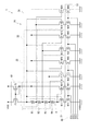
本発明の第1実施形態に係る定電流回路1を添付図面に基づいて説明する。図1は、第1実施形態の定電流回路1の回路図である。
定電流回路1は、第1カレントミラー回路10と、複数(本実施形態では4つ)の第2カレントミラー回路20(21〜24)と、定電流調整回路30と、制御信号出力回路40とを備える。
[First Embodiment]
A constant
The constant
第1カレントミラー回路10は、第1および第2のPチャネル型(Pch)の電界効果型トランジスター(MOSFET:metal-oxide-semiconductor field-effect transistor)P1、P2を備えている。ここで、第1の電界効果型トランジスターP1によって、第1回路用第1トランジスターが構成され、第2の電界効果型トランジスターP2によって、第1回路用第2トランジスターが構成されている。
第1の電界効果型トランジスターP1のソースは、第1電源である高電位側電源VDDに接続され、ドレインは、後述する第2カレントミラー回路21〜24の定電流調整用抵抗Rに接続され、ゲートは、第2の電界効果型トランジスターP2のゲートに接続されている。
第2の電界効果型トランジスターP2は、ドレインとゲートとが接続されたダイオード結合となっている。第2の電界効果型トランジスターP2のソースは、高電位側電源VDDに接続され、ドレインは、第2カレントミラー回路21〜24に接続され、ゲートは、第1の電界効果型トランジスターP1のゲートに接続されている。
The first
The source of the first field effect transistor P1 is connected to the high potential side power supply VDD which is the first power supply, and the drain is connected to a constant current adjusting resistor R of second
The second field effect transistor P2 has a diode coupling in which a drain and a gate are connected. The source of the second field effect transistor P2 is connected to the high potential side power supply VDD, the drain is connected to the second
第2カレントミラー回路20は、1番目(N=1)から4番目(N番目)まで4個(N個)の第2カレントミラー回路21〜24を備えている。各第2カレントミラー回路21〜24は、定電流調整用抵抗Rと、第1および第2のNチャネル型(Nch)の電界効果型トランジスターN1,N2とを備えている。
ここで、定電流調整用抵抗Rは、第1抵抗R1から第4抵抗(第N抵抗)R4まで4個(N個)の定電流調整用抵抗を備えている。本実施形態では、第1抵抗R1〜第4抵抗R4は、ポリシリコンで構成されている。
また、第1の電界効果型トランジスターN1(N11〜N14)によって、第2回路用第1トランジスターが構成され、第2の電界効果型トランジスターN2(N21〜N24)によって、第2回路用第2トランジスターが構成されている。
The second
Here, the constant current adjusting resistor R includes four (N) constant current adjusting resistors from the first resistor R1 to the fourth resistor (Nth resistor) R4. In the present embodiment, the first resistor R1 to the fourth resistor R4 are made of polysilicon.
The first transistor for the second circuit is configured by the first field effect transistor N1 (N11 to N14), and the second transistor for the second circuit is configured by the second field effect transistor N2 (N21 to N24). Is configured.
1番目の第2カレントミラー回路21は、定電流調整用抵抗Rと、第1の電界効果型トランジスターN11と、第2の電界効果型トランジスターN21とを備え、定電流調整用抵抗Rは、第1抵抗R1から第4抵抗R4まで4個の抵抗が直列に接続されて構成されている。
2番目の第2カレントミラー回路22は、定電流調整用抵抗Rと、第1の電界効果型トランジスターN12と、第2の電界効果型トランジスターN22とを備え、定電流調整用抵抗Rは、第1抵抗R1から第3抵抗R3まで3個の抵抗が直列に接続されて構成されている。
3番目の第2カレントミラー回路23は、定電流調整用抵抗Rと、第1の電界効果型トランジスターN13と、第2の電界効果型トランジスターN23とを備え、定電流調整用抵抗Rは、第1抵抗R1から第2抵抗R2まで2個の抵抗が直列に接続されて構成されている。
4番目の第2カレントミラー回路24は、定電流調整用抵抗Rと、第1の電界効果型トランジスターN14と、第2の電界効果型トランジスターN24とを備え、定電流調整用抵抗Rは、第1抵抗R1の1個の抵抗で構成されている。
したがって、k番目(kは1以上、N以下の整数)の第2カレントミラー回路の定電流調整用抵抗Rは、第1抵抗から第k抵抗までk個の抵抗が直列に接続されて構成されている。
The first second
The second second
The third second
The fourth second
Therefore, the constant current adjusting resistor R of the k-th (k is an integer not less than 1 and not more than N) second current mirror circuit is configured by connecting k resistors in series from the first resistor to the k-th resistor. ing.
第2カレントミラー回路21〜24において、第1の電界効果型トランジスターN11〜N14のドレインは、定電流調整用抵抗Rに接続され、ソースは、定電流調整回路30に接続され、ゲートは、第1の電界効果型トランジスターP1のドレインに接続されている。
第2カレントミラー回路21〜24において、第2の電界効果型トランジスターN21〜N24のドレインは、第2の電界効果型トランジスターP2のドレインに接続され、ソースは、定電流調整回路30に接続され、ゲートは、定電流調整用抵抗Rつまり第1の電界効果型トランジスターN11〜N14のドレインに接続されている。
In the second
In the second
定電流調整回路30は、カレントミラー回路21〜24と、低電位側電源VSSとの間を断続する複数のスイッチを備えて構成されている。
具体的には、定電流調整回路30は、第1の電界効果型トランジスターN11〜N14と低電位側電源VSSとを断続するスイッチであるNチャネル型の電界効果型トランジスターN31〜N34と、第2の電界効果型トランジスターN21〜N24と低電位側電源VSSとを断続するスイッチであるNチャネル型の電界効果型トランジスターN41〜N44とを備えている。このため、電界効果型トランジスターN31〜N34によって第1スイッチ用トランジスターが構成され、電界効果型トランジスターN41〜N44によって第2スイッチ用トランジスターが構成される。
The constant
Specifically, the constant
電界効果型トランジスターN31〜N34のドレインは、電界効果型トランジスターN11〜N14のソースに接続され、ソースは、低電位側電源VSSに接続され、ゲートは、電界効果型トランジスターN41〜N44のゲートに接続されている。
電界効果型トランジスターN41〜N44のドレインは、電界効果型トランジスターN21〜N24のソースに接続され、ソースは、低電位側電源VSSに接続され、ゲートは、電界効果型トランジスターN31〜N34のゲートに接続されている。
また、電界効果型トランジスターN31〜34と、電界効果型トランジスターN41〜N44とは、同じサイズで構成されている。
The drains of the field effect transistors N31 to N34 are connected to the sources of the field effect transistors N11 to N14, the sources are connected to the low potential power source VSS, and the gates are connected to the gates of the field effect transistors N41 to N44. Has been.
The drains of the field effect transistors N41 to N44 are connected to the sources of the field effect transistors N21 to N24, the sources are connected to the low potential power source VSS, and the gates are connected to the gates of the field effect transistors N31 to N34. Has been.
The field effect transistors N31 to N34 and the field effect transistors N41 to N44 are configured to have the same size.
制御信号出力回路40は、図示しないレベルシフターを備えており、定電圧レベルの制御信号SEL1〜SEL4を定電流調整回路30に出力する。
電界効果型トランジスターN31、N41のゲートには、制御信号出力回路40から出力される定電圧の制御信号SEL1が入力される。この制御信号SEL1によって、電界効果型トランジスターN31、N41は同時にオン、オフされる。
電界効果型トランジスターN32、N42のゲートには、制御信号出力回路40から出力される定電圧の制御信号SEL2が入力される。この制御信号SEL2によって、電界効果型トランジスターN32、N42は同時にオン、オフされる。
電界効果型トランジスターN33、N43のゲートには、制御信号出力回路40から出力される定電圧の制御信号SEL3が入力される。この制御信号SEL3によって、電界効果型トランジスターN33、N43は同時にオン、オフされる。
電界効果型トランジスターN34、N44のゲートには、制御信号出力回路40から出力される定電圧の制御信号SEL4が入力される。この制御信号SEL4によって、電界効果型トランジスターN34、N44は同時にオン、オフされる。
The control
A constant voltage control signal SEL1 output from the control
A constant voltage control signal SEL2 output from the control
A constant voltage control signal SEL3 output from the control
A constant voltage control signal SEL4 output from the control
従って、制御信号出力回路40は、制御信号SEL1〜SEL4のいずれか1つをNchの電界効果型トランジスターのオン信号とし、残りをオフ信号とすることで、第2カレントミラー回路21〜24の中から1つの第2カレントミラー回路を選択して作動できる。
Therefore, the control
次に、本実施形態の第1カレントミラー回路10および第2カレントミラー回路21〜24による定電流回路1の動作について、図2を参照して説明する。図2は、図1において、制御信号SEL1がオン信号とされ、他の制御信号SEL2〜SEL4がオフ信号とされた場合の等価回路である。
制御信号SEL1がオン信号であり、電界効果型トランジスターN31、N41がオンされると、図2に示す、第1カレントミラー回路10と、第2カレントミラー回路21とを有する、自己バイアス永田基準電流回路として知られる定電流回路1が構成される。
本実施形態では、第1カレントミラー回路10の第1の電界効果型トランジスターP1のβをβP1とし、第2の電界効果型トランジスターP2のβをβP2とすると、βP1=βP2である。ここで、βはMOSトランジスターの特性を表すパラメーターの1つであり、チャネル幅をW、チャネル長をL、移動度をμ、ゲート酸化膜の単位面積当たりの容量をCoxとすると、β=(W/L)・μ・Coxで求められる。
Next, the operation of the constant
When the control signal SEL1 is an on signal and the field effect transistors N31 and N41 are turned on, the self-biased Nagata reference current having the first
In the present embodiment, when β of the first field effect transistor P1 of the first
また、第2カレントミラー回路21の第1の電界効果型トランジスターN11のβをβN11、第2の電界効果型トランジスターN21のβをβN21とすると、βN11<βN21である。そして、定電流調整用抵抗Rの抵抗値をRとすると、定電流Idは次の式(1)で表される。
Further, when β of the first field effect transistor N11 of the second

前記式(1)を見ても明らかであるが、抵抗Rの製造バラツキによって定電流Idの値が変動する。そのため、所望の定電流を得るためには、抵抗の切り替え回路が必要である。本実施形態では、図1に示すように、制御信号SEL1〜SEL4によって定電流調整回路30を制御することで、複数の第2カレントミラー回路21〜24を切り替えている。これにより、定電流調整用抵抗Rを、4つの抵抗R1〜R4が直列に接続された状態から、1つの抵抗R1のみで構成された状態まで、4段階に抵抗値を切り替えることができ、これにより所望の定電流を得ることができる。
As apparent from the equation (1), the value of the constant current Id varies depending on the manufacturing variation of the resistor R. Therefore, in order to obtain a desired constant current, a resistance switching circuit is required. In this embodiment, as shown in FIG. 1, the plurality of second
すなわち、制御信号出力回路40によって制御信号SEL1をオン信号とし、他をオフ信号とすれば、定電流回路1は、第1カレントミラー回路10と、第2カレントミラー回路21とで構成され、定電流調整用抵抗Rは、直列に接続された4つの抵抗R1〜R4で構成される。
制御信号出力回路40によって制御信号SEL2をオン信号とし、他をオフ信号とすれば、定電流回路1は、第1カレントミラー回路10と、第2カレントミラー回路22とで構成され、定電流調整用抵抗Rは、直列に接続された3つの抵抗R1〜R3で構成される。
制御信号出力回路40によって制御信号SEL3をオン信号とし、他をオフ信号とすれば、定電流回路1は、第1カレントミラー回路10と、第2カレントミラー回路23とで構成され、定電流調整用抵抗Rは、直列に接続された2つの抵抗R1〜R2で構成される。
制御信号出力回路40によって制御信号SEL4をオン信号とし、他をオフ信号とすれば、定電流回路1は、第1カレントミラー回路10と、第2カレントミラー回路24とで構成され、定電流調整用抵抗Rは、直列に接続された1つの抵抗R1で構成される。
That is, if the control signal SEL1 is turned on by the control
If the control signal SEL2 is turned on by the control
If the control signal SEL3 is turned on by the control
If the control signal SEL4 is turned on by the control
定電流回路1において、各制御信号SEL1〜SEL4を順次オン信号として、第1カレントミラー回路10と、第2カレントミラー回路21〜24とを組み合わせた際の定電流を検出する。そして、所望の定電流が得られた際の制御信号SEL1〜SEL4の設定を、不揮発性メモリーに書き込んだり、IC内部の制御回路で形成できるようにしておく。これにより、定電流回路1を作動させた際に、制御信号出力回路40は、前記不揮発性メモリーの設定データを読み込んだりすることで、設定された制御信号SEL1〜SEL4を出力でき、電源電圧の変動に影響されずに、定電流回路1から所望の定電流Idを得ることができる。
In the constant
[第1実施形態の効果]
このような第1実施形態によれば、次のような効果がある。
定電流回路1を、第1カレントミラー回路10と、複数の第2カレントミラー回路21〜24とを備えて構成し、定電流調整回路30のスイッチ素子である電界効果型トランジスターN31〜N34,N41〜N44を、制御信号出力回路40から出力される定電圧レベルの制御信号SEL1〜SEL4でオン、オフ制御することで、定電流調整用抵抗Rの抵抗値を4段階に切り替えることができる。したがって、抵抗の製造バラツキがあっても、第2カレントミラー回路21〜24から作動する回路を選択することで、所望の定電流を得ることができる。
[Effect of the first embodiment]
According to such 1st Embodiment, there exist the following effects.
The constant
制御信号出力回路40は、定電圧レベルの制御信号SEL1〜SEL4を出力しているので、定電流調整回路30の各電界効果型トランジスターN31〜N34,N41〜N44のゲートに印加される前記制御信号SEL1〜SEL4が、電源電圧の変動による影響を受けずに一定レベルになるため、各電界効果型トランジスターN31〜N34,N41〜N44のON抵抗の変化が無く、ON抵抗の変動によって定電流値が変化することを防止できる。
Since the control
複数の第2カレントミラー回路21〜24において、一部の抵抗R1〜R3は、複数の第2カレントミラー回路21〜24で共通して利用できるので、各第2カレントミラー回路において、別々の抵抗を設ける場合に比べて、抵抗の配置スペースを小さくでき、ICの面積を小さくする事ができる。ICの面積を小さくする事で、ICを実装する基板上に効率的に配置する事が可能になり、ICコストも低減できる。
In the plurality of second
定電流回路1は、第2カレントミラー回路21〜24と、低電位側電源VSSとの間に定電流調整回路30を接続しているので、定電流調整回路30を構成する電界効果型トランジスターN31〜N34、N41〜N44のゲートとソース間の電位が、電界効果型トランジスターN31〜N34、N41〜N44の閾値電圧Vthより大きくなるように回路を構成し易くなる。これにより、低い電源電圧で駆動する場合でも、トランジスターの電流を流す能力を大きくできるため、腕時計のような低電圧で駆動する必要のあるデバイスに定電流回路1を組み込む際に非常に効果がある。また、スイッチング回路の面積を大きくする必要もなくなるため、ICの面積を小さくする事ができ、ICを実装する基板上に効率的に配置する事が可能になり、ICコストも低減できる。
Since the constant
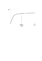
さらに、カレントミラー回路では、カレントミラー回路を駆動する電源電圧を大きくすると、チャネル長変調の影響が大きくなるため、電源電圧が大きくなるほど、定電流値は大きくなってしまう。すなわち、図3に示すように、カレントミラー回路を駆動する電源電圧をVds、定電流値Idsとすると、電源電圧を定電圧Vd1で一定とすれば、チャネル長変調の影響を受けることが無くなり、定電流値Idsも一定値となるため、より電源電圧の変動に影響を受けない定電流を得られる。 Further, in the current mirror circuit, if the power supply voltage for driving the current mirror circuit is increased, the influence of channel length modulation increases, so that the constant current value increases as the power supply voltage increases. That is, as shown in FIG. 3, when the power supply voltage for driving the current mirror circuit is Vds and the constant current value Ids, if the power supply voltage is constant at the constant voltage Vd1, the channel length modulation is not affected. Since the constant current value Ids is also a constant value, a constant current that is more unaffected by fluctuations in power supply voltage can be obtained.
さらに、定電流調整回路30に使用している電界効果型トランジスターN31〜N34、N41〜N44のサブストレイト(SUB)を定電圧電源に接続することで、バックゲート効果による閾値電圧Vthの変動を受けずに、より電源電圧の変動に影響を受けない定電流を得ることができる。
Further, by connecting the substrate (SUB) of the field effect transistors N31 to N34 and N41 to N44 used in the constant
定電流調整回路30の対となる電界効果型トランジスターN31〜N34と、電界効果型トランジスターN41〜N44とは、同じサイズで構成されているので、トランジスターのON抵抗が同じになり、定電流回路1を設計する際に、トランジスターのON抵抗の違いを考慮しなくても良く、容易に設計できる。
Since the field effect transistors N31 to N34 and the field effect transistors N41 to N44 that are paired with the constant
また、定電流調整用抵抗R1〜R4は、電圧依存性の小さいポリシリコンで構成されているので、電源電圧の変動にさらに影響を受けない定電流を得ることができる。すなわち、一般的に、抵抗はポリシリコンや拡散により構成される。ただし、拡散により構成された抵抗は、電源電圧によって抵抗値が変動してしまう。ポリシリコン抵抗は電源電圧の変動による抵抗の変化が小さいため、定電流調整用抵抗R1〜R4をポリシリコンで構成することで、より電源電圧の変動に影響を受けない定電流を得られる。
さらに、定電流回路1を定電圧駆動した場合でも、時計用IC110の他の部分が定電圧駆動になっていない限り、電源電圧の影響を受けて抵抗値が変動してしまう。従って、この点でも、定電流調整用抵抗R1〜R4は、ポリシリコンで構成することが好ましい。
Further, since the constant current adjusting resistors R1 to R4 are made of polysilicon having a small voltage dependency, it is possible to obtain a constant current that is not further affected by fluctuations in the power supply voltage. That is, generally, the resistor is constituted by polysilicon or diffusion. However, the resistance value of the resistor formed by diffusion varies depending on the power supply voltage. Since the resistance change of the polysilicon resistor due to the fluctuation of the power supply voltage is small, the constant current adjustment resistors R1 to R4 are made of polysilicon to obtain a constant current that is more unaffected by the fluctuation of the power supply voltage.
Further, even when the constant
[第2実施形態]
図4は、第2実施形態の定電流回路1Aの構成を示す回路図である。なお、定電流回路1Aにおいて、第1実施形態の定電流回路1と同一または同様の構成には同一符号を付して説明を簡略する。
定電流回路1Aは、第1電源を低電位側電源VSSとし、第2電源を高電位側電源VDDとしたものである。このため、第1カレントミラー回路10Aは、Nchの電界効果型トランジスターN1,N2で構成され、複数の第2カレントミラー回路21A〜24Aは、Pchの電界効果型トランジスターP11〜P14,P21〜P24で構成されている。
第1カレントミラー回路10Aは、低電位側電源VSSに接続され、定電流調整回路30Aは、高電位側電源VDDとカレントミラー回路21A〜24Aとの間に接続されている。
定電流調整回路30Aは、Pchの電界効果型トランジスターP31〜P34,P41〜P44を備えて構成され、制御信号出力回路40からの制御信号SEL1〜SEL4で制御されている。
[Second Embodiment]
FIG. 4 is a circuit diagram showing a configuration of a constant
In the constant
The first
The constant
[第2実施形態の効果]
このような定電流回路1Aにおいても、制御信号出力回路40から出力される制御信号SEL1〜SEL4によって、第1カレントミラー回路10Aと、第2カレントミラー回路21A〜24Aから選択した回路とで定電流回路1Aを構成でき、定電流調整用抵抗Rを4段階に切り替えることができる。したがって、前記第1実施形態の定電流回路1と同じ作用効果を奏することができる。
[Effects of Second Embodiment]
Also in such a constant
[第3実施形態]
次に、第1実施形態の定電流回路1を用いた温度センサー2と、この温度センサー2を用いた温度補償機能付き時計100に関する第3実施形態を、図5,6を参照して説明する。
[Third Embodiment]
Next, a third embodiment relating to a
[温度補償機能付き時計]
図5は、温度補償機能付き時計100の構成を示すブロック図が示されている。
温度補償機能付き時計100は、電源102と、電源102によって駆動する時計用IC110と、水晶振動子104と、ステップモーター105とを備えている。
[Clock with temperature compensation function]
FIG. 5 is a block diagram showing the configuration of the
The timepiece with
電源102は、一次電池や二次電池で構成される。なお、二次電池を用いた場合には、温度補償機能付き時計100に二次電池を充電する発電機を設けたり、温度補償機能付き時計100の外部から充電できるように構成すればよい。発電機は、太陽電池や、回転錘で発電する発電機などの時計用の発電機が利用できる。
ステップモーター105は、図示しない輪列を介して、分針、秒針、時針等の指針を駆動する。従って、温度補償機能付き時計100は、アナログ式の時計である。
The
The
時計用IC110は、水晶発振回路用定電圧回路111と、発振装置120と、分周回路112と、モーターパルス形成回路113と、温度センサー制御回路130と、温度センサー用定電圧回路131と、温度センサー2と、演算回路141と、周波数調整制御回路142とを備えている。温度センサー制御回路130および温度センサー2間には、図示略のレベルシフター(L/S)が配置され、温度センサー制御回路130から温度センサー2に入力される制御信号を定電圧の信号としている。
The
水晶発振回路用定電圧回路111は、電源102の電源電圧を定電圧に変換し、発振装置120に供給する。
発振装置120は、発振回路121と、周波数調整回路122と、レベルシフター(L/S)123と、波形成形回路125とを備えている。
発振回路121は、水晶振動子104を発振させるための一般的な回路であり、例えば、発振インバーターと、帰還抵抗と、ゲートコンデンサーと、ドレインコンデンサーとを備えるものなどが利用できる。
発振回路121は、発振源である水晶振動子104を駆動して源振となる32kHz(32768Hz)の発振信号を波形成形回路125に出力する。この際、周波数調整回路122によって発振信号の周波数を調整している。
波形成形回路125は、波形成形用インバーターなどで構成され、発振回路121から出力された発振信号を成形してクロック信号として分周回路112に出力する。
The crystal oscillation circuit
The
The
The
The
分周回路112は、時計用IC110で用いられる一般的な分周回路であり、複数の分周器を備え、前記発振信号を一定周期(例えば1Hz)まで分周し、時間計測の基準となる基準信号として出力する。
モーターパルス形成回路113は、分周回路112から出力される信号を用いてステップモーター105を駆動するモーターパルスを形成して出力する。このモーターパルスは、モーターパルス形成回路113からステップモーター105に出力され、ステップモーター105が駆動される。このステップモーター105の駆動により、輪列を介して指針が運針し、時刻が表示される。したがって、モーターパルス形成回路113、ステップモーター105および図示しない輪列、指針を備えて時刻表示部107が構成される。
The
The motor
分周回路112から出力されるクロック信号は、温度センサー制御回路130にも入力される。温度センサー制御回路130は、前記クロック信号の入力によって所定のタイミングで温度センサー2と、温度センサー用定電圧回路131とを駆動する。この際、温度センサー制御回路130から温度センサー2に出力される制御信号は、レベルシフター(図示略)によって定電圧の制御信号とされ、この定電圧の制御信号で温度センサー2が駆動される。
The clock signal output from the
[温度センサー]
温度センサー2は、前記定電流回路1と、CR発振回路60とを備えて構成され、CR発振回路60の温度特性によって変化する発振周波数に基づいて、時計用IC110が配置された空間(時計ケース内)の温度を測定する。
[Temperature sensor]
The
この温度センサー2の詳細について、図6を参照して説明する。
温度センサー2は、第1実施形態の定電流回路1と、CR発振回路60と、出力バッファー90とを備えている。温度センサー2において、高電位側電源VDDおよび低電位側電源VSSの少なくとも一方は、温度センサー用定電圧回路131による定電圧とされ、定電流回路1も定電圧で駆動される。本実施形態では、温度センサー用定電圧回路131が出力する高電位側電源VDDは、電源102の電源電圧よりも低い電圧レベルとし、電源電圧が変動しても、高電位側電源VDDは一定の電圧レベルに維持している。また、低電位側電源VSSはグランド電圧であるため、定電圧である。
Details of the
The
[CR発振回路の構成]
CR発振回路60は、コンデンサー(C)及び抵抗(R)により構成される回路であり、予め設定された周波数の発振信号を出力する。本実施形態のCR発振回路60は、図6に示すように、3段のインバーター61,62,63で構成されており、各段のインバーター61〜63を構成するPchの電界効果型トランジスター611,621,631のソースは、定電流を供給するためのカレントミラー回路のPchの電界効果型トランジスター80を介して高電位側電源VDDに接続され、Nchの電界効果型トランジスター612,622,632のソースは、低電位側電源VSSに接続されている。
インバーター61のドレインには、抵抗641と、コンデンサー651が直列に接続されている。抵抗641とコンデンサー651の間の接続点は、インバーター62のゲートに接続されている。
インバーター62のドレインには、抵抗642と、コンデンサー652が直列に接続され、この間の接続点は、インバーター63のゲートに接続されている。
インバーター63のドレインには、抵抗643と、コンデンサー653が直列に接続され、この間の接続点は、出力バッファー90のゲートに接続され、さらにインバーター61のゲートに接続されている。
出力バッファー90は、Pchの電界効果型トランジスター91およびNchの電界効果型トランジスター92を備えたインバーターである。
[Configuration of CR oscillation circuit]
The
A
A
A
The
各コンデンサー651〜653の一端は、低電位側電源VSSに接続されている。出力バッファー90からの出力は、CR発振回路60で発振された発振信号の出力であり、温度センサー2の出力として演算回路141に入力される。
One end of each of the
CR発振回路60の発振信号の周波数は、各コンデンサー651〜653に充電される電荷の充放電速度により決定する。よって、各インバーター61〜63のドレインと、グランド電圧VSS間に直列に接続されている抵抗(放電抵抗)641〜643と、コンデンサー651〜653の値と、定電流回路1から供給される定電流によって発振周波数が決定する。
なお、CR発振回路60の抵抗641〜643は、定電流回路1の定電流調整用抵抗R1〜R4と同じ種類であるポリシリコンで構成されている。
The frequency of the oscillation signal of the
The
定電流回路1を構成する抵抗R1〜R4や、CR発振回路60を構成する抵抗641〜643やコンデンサー651〜653等の素子は温度特性を有しているため、CR発振回路60に供給される定電流は温度によって変化し、CR発振回路60から出力される発振信号の周波数は、温度によって変化する。この温度特性を利用することで、定電流回路1とCR発振回路60とを組み合わせて温度センサー2を構成できる。
Since the resistors R1 to R4 constituting the constant
また、電界効果型トランジスター80のゲートには、定電流回路1の出力が接続されていて、トランジスターP2とトランジスター80とでカレントミラー回路を構成している。このため、温度センサー2における温度検出部であるCR発振回路60は、定電流回路1の定電流バイアスで駆動する。定電流回路1の定電流は、第1実施形態と同じく制御信号出力回路40からの制御信号SEL1〜SEL4により制御され、温度センサー2のCR発振回路60を適切な定電流デバイスで駆動できるように設定されている。
The output of the constant
図5に示すように、温度センサー2の出力(温度情報となる発振周波数)は演算回路141に入力される。演算回路141は、温度センサー2で測定された温度(CR発振回路60の発振周波数)に基づいて、発振装置120から出力される発振信号の周波数の補正量を算出し、その演算結果を周波数調整制御回路142に入力する。
周波数調整制御回路142は、前記演算結果に基づいて周波数調整回路122を制御する制御信号を出力する。この際、周波数調整制御回路142から出力された制御信号は、レベルシフター123により定電圧化され、周波数調整回路122に入力される。
As shown in FIG. 5, the output of the temperature sensor 2 (the oscillation frequency serving as temperature information) is input to the
The frequency
周波数調整回路122は、前記制御信号によって、発振回路121から出力される発振信号の周波数を調整する。周波数調整回路122は、例えば、発振回路121に接続する調整用容量(コンデンサー)の接続時間を変化させたり、発振回路121に接続する調整用容量の個数を変化させることで、発振回路121から出力される発振信号の周波数を調整するものなど、従来から用いられている周波数調整回路122を利用できる。
したがって、発振装置120は、周波数調整回路122により調整された周波数の発振信号を出力する。
The
Therefore, the
[第3実施形態の効果]
温度センサー2は、温度特性を有するCR発振回路60を、定電流回路1の定電流バイアスで駆動できるため、電源102の電源電圧が変動しても、温度センサー2の検出温度が変動しないため、温度センサー2は正確な温度情報を出力できる。
例えば、温度センサー2の電源電圧による検出温度の変動を実験したところ、従来技術では、電源電圧が1.58Vから1.20Vに変化した場合に、約10℃の検出温度の差が発生していた。これに対し、本実施形態では、約-0.1℃しか検出温度が変化せず、電源電圧が変動しても検出温度の変動を抑制でき、正確な温度情報を出力できることを確認できた。
このため、演算回路141で算出される補正量は、電源電圧に影響されずに正確になり、周波数調整制御回路142によって周波数調整回路122を調整することで、発振装置120から出力される発振信号の周波数を、電源電圧の変動に影響されずに一定に維持できる。このため、温度補償機能付き時計100は、電池(電源102)の放電末期まで高精度を保つことができ、年差時計にも適用できる。
[Effect of the third embodiment]
Since the
For example, when the variation of the detected temperature due to the power supply voltage of the
Therefore, the correction amount calculated by the
温度センサー2は、CR発振回路60の発振周波数によって温度を検出しているので、時計用IC110内部の演算回路141における演算処理がし易くなり、周波数調整制御回路142および周波数調整回路122による補正処理も容易に行うことができる。
Since the
温度センサー2において、定電流回路1の定電流調整用抵抗R1〜R4と、CR発振回路60の抵抗641〜643は、同じ種類(例えばポリシリコン)で構成しているので、温度に対する抵抗の変化を同じ傾きにできる。
このため、定電流調整用抵抗R1〜R4、抵抗641〜643の各抵抗の温度特性が、温度が高くなるほど抵抗値が小さくなり、温度が低くなるほど抵抗値が大きくなる特性であった場合、温度が高くなると、定電流回路1では定電流は大きくなり、CR発振回路60では電荷の放電速度が速くなるため、発振周波数が大きくなる。反対に温度が低くなると、定電流回路1では定電流は小さくなり、CR発振回路60では電荷の放電速度が遅くなるため、発振周波数が小さくなる。
一方、定電流調整用抵抗R1〜R4、抵抗641〜643の各抵抗の温度特性が、温度が高くなるほど抵抗値が大きくなり、温度が低くなるほど抵抗値が小さくなる特性であった場合、温度が高くなると、定電流回路1では定電流は小さくなり、CR発振回路60では電荷の放電速度が遅くなるため、発振周波数が小さくなる。反対に温度が低くなると、定電流回路1では定電流は大きくなり、CR発振回路60では電荷の放電速度が速くなるため、発振周波数が大きくなる。
つまり、温度特性の傾きの符号が同じ抵抗を使用することにより、定電流回路1とCR発振回路60の双方で温度特性を重ね合わせることが可能となり、温度センサー2の出力である発振周波数の温度傾きを大きくできる。温度センサー2の特性として、温度に対して傾きが大きいほど高感度の温度センサー2とすることができる。
In the
Therefore, if the temperature characteristics of the constant current adjusting resistors R1 to R4 and
On the other hand, if the temperature characteristics of the constant current adjusting resistors R1 to R4 and
That is, by using resistors having the same sign of the temperature characteristic slope, it is possible to superimpose the temperature characteristic in both the constant
[変形例]
なお、本発明は、前記実施形態に限定されるものではなく、本発明の目的を達成できる他の構成も含み、以下に示すような変形例等も本発明に含まれる。
例えば、温度センサー2における定電流回路1としては、第2実施形態の定電流回路1Aを用いてもよい。
[Modification]
In addition, this invention is not limited to the said embodiment, Other structures which can achieve the objective of this invention are included, and the modification etc. which are shown below are also contained in this invention.
For example, as the constant
また、本発明の温度センサー2は、温度補償機能付き時計100に用いられるものに限定されず、温度測定が必要な機器に適用できる。特に、本発明の温度センサー2は、定電流回路1およびCR発振回路60で構成されるため、IC内部に組み込むことができ、様々な機器に適用できる。
The
さらに、定電流回路1の定電流調整用抵抗R1〜R4と、CR発振回路60の抵抗641〜643とは同じ種類の抵抗とすることが好ましいが、種類が異なる抵抗を用いてもよい。また、これらの抵抗R1〜R4、641〜643は、ポリシリコンで構成されることが好ましいが、ポリシリコンに限定されるものではない。
Furthermore, the constant current adjusting resistors R1 to R4 of the constant
定電流回路1、1Aにおいて、第2カレントミラー回路21〜24,21A〜24Aの数は4個に限定されず、2個あるいは3個でもよく、5個以上でもよい。
In the constant
1、1A…定電流回路、2…温度センサー、10、10A…第1カレントミラー回路、21〜24、21A〜24A…第2カレントミラー回路、30、30A…定電流調整回路、40…制御信号出力回路、60…CR発振回路、80…電界効果型トランジスター、90…出力バッファー、100…温度補償機能付き時計、102…電源、104…水晶振動子、105…ステップモーター、107…時刻表示部、110…時計用IC、111…水晶発振回路用定電圧回路、112…分周回路、113…モーターパルス形成回路、120…発振装置、121…発振回路、122…周波数調整回路、125…波形成形回路、130…温度センサー制御回路、131…温度センサー用定電圧回路、141…演算回路、142…周波数調整制御回路、N11〜N14…第1の電界効果型トランジスター、N21〜N24…第2の電界効果型トランジスター、N31〜N34…電界効果型トランジスター、N41〜N44…電界効果型トランジスター、P1…第1の電界効果型トランジスター、P2…第2の電界効果型トランジスター、R…定電流調整用抵抗、R1…第1抵抗、R2…第2抵抗、R3…第3抵抗、R4…第4抵抗、SEL1〜SEL4…制御信号、VDD…高電位側電源、VSS…低電位側電源。
DESCRIPTION OF
Claims (7)
前記第1カレントミラー回路に接続された複数の第2カレントミラー回路と、
前記高電位側電源および前記低電位側電源の他方の電源である第2電源と、複数の前記第2カレントミラー回路との間に接続されたトランジスターで構成された複数のスイッチを備える定電流調整回路と、
複数の前記スイッチの動作を制御する定電圧レベルの制御信号を出力する制御信号出力回路と、を備え、
前記第1カレントミラー回路は、第1回路用第1トランジスターと、第1回路用第2トランジスターとを備え、
複数の前記第2カレントミラー回路は、
定電流調整用抵抗と、
前記第1回路用第1トランジスターに、前記定電流調整用抵抗を介して接続された第2回路用第1トランジスターと、
前記第1回路用第2トランジスターに接続された第2回路用第2トランジスターと、をそれぞれ備え、
複数の前記第2カレントミラー回路における前記定電流調整用抵抗の抵抗値はそれぞれ異なり、
前記制御信号出力回路は、
前記スイッチをオンするための前記制御信号を出力して、複数の前記第2カレントミラー回路から1つの第2カレントミラー回路を作動させる
ことを特徴とする定電流回路。 A first current mirror circuit connected to a first power source which is one of a high potential side power source and a low potential side power source;
A plurality of second current mirror circuits connected to the first current mirror circuit;
Constant current adjustment comprising a plurality of switches composed of transistors connected between a second power source that is the other power source of the high potential side power source and the low potential side power source and a plurality of the second current mirror circuits Circuit,
A control signal output circuit for outputting a control signal at a constant voltage level for controlling the operation of a plurality of the switches,
The first current mirror circuit includes a first transistor for a first circuit and a second transistor for a first circuit,
The plurality of second current mirror circuits include:
A constant current adjusting resistor;
A first transistor for a second circuit connected to the first transistor for a first circuit via the constant current adjusting resistor;
A second circuit second transistor connected to the first circuit second transistor, respectively.
The resistance values of the constant current adjusting resistors in the plurality of second current mirror circuits are different from each other,
The control signal output circuit is
A constant current circuit, wherein the control signal for turning on the switch is output to operate one second current mirror circuit from the plurality of second current mirror circuits.
前記第1電源は前記高電位側電源であり、前記第2電源は前記低電位側電源であり、
前記第1回路用第1トランジスターおよび前記第1回路用第2トランジスターは、Pチャネル型の電界効果型トランジスターで構成され、
前記第2回路用第1トランジスターおよび前記第2回路用第2トランジスターは、Nチャネル型の電界効果型トランジスターで構成され、
前記定電流調整回路の前記スイッチは、Nチャネル型の電界効果型トランジスターで構成され、
前記第2カレントミラー回路は、1番目からN番目(Nは2以上の整数)までN個設けられ、
前記定電流調整用抵抗は、第1抵抗から第N抵抗までN個の抵抗を備え、
k番目(kは1以上、N以下の整数)の第2カレントミラー回路の前記定電流調整用抵抗は、第1抵抗から第k抵抗までk個の抵抗が直列に接続されている
ことを特徴とする定電流回路。 The constant current circuit according to claim 1,
The first power source is the high potential side power source, the second power source is the low potential side power source,
The first transistor for the first circuit and the second transistor for the first circuit are composed of P-channel field effect transistors,
The first transistor for the second circuit and the second transistor for the second circuit are composed of N-channel field effect transistors,
The switch of the constant current adjustment circuit is composed of an N-channel field effect transistor,
N second current mirror circuits are provided from the first to the Nth (N is an integer of 2 or more),
The constant current adjusting resistor includes N resistors from a first resistor to an Nth resistor,
The constant current adjusting resistor of the k-th (k is an integer not less than 1 and not more than N) second current mirror circuit is characterized in that k resistors from the first resistor to the k-th resistor are connected in series. A constant current circuit.
前記第1電源は前記低電位側電源であり、前記第2電源は前記高電位側電源であり、
前記第1回路用第1トランジスターおよび前記第1回路用第2トランジスターは、Nチャネル型の電界効果型トランジスターで構成され、
前記第2回路用第1トランジスターおよび前記第2回路用第2トランジスターは、Pチャネル型の電界効果型トランジスターで構成され、
前記定電流調整回路の前記スイッチは、Pチャネル型の電界効果型トランジスターで構成され、
前記第2カレントミラー回路は、1番目からN番目(Nは2以上の整数)までN個設けられ、
前記定電流調整用抵抗は、第1抵抗から第N抵抗までN個の抵抗を備え、
k番目(kは1以上、N以下の整数)の第2カレントミラー回路の前記定電流調整用抵抗は、第1抵抗から第k抵抗までk個の抵抗が直列に接続されている
ことを特徴とする定電流回路。 The constant current circuit according to claim 1,
The first power source is the low potential side power source, the second power source is the high potential side power source,
The first circuit first transistor and the first circuit second transistor are N-channel field effect transistors,
The first transistor for the second circuit and the second transistor for the second circuit are composed of P-channel field effect transistors,
The switch of the constant current adjustment circuit is composed of a P-channel field effect transistor,
N second current mirror circuits are provided from the first to the Nth (N is an integer of 2 or more),
The constant current adjusting resistor includes N resistors from a first resistor to an Nth resistor,
The constant current adjusting resistor of the k-th (k is an integer not less than 1 and not more than N) second current mirror circuit is characterized in that k resistors from the first resistor to the k-th resistor are connected in series. A constant current circuit.
前記定電流調整回路の複数のスイッチは、
前記第2回路用第1トランジスターおよび前記第2電源との間に配置された第1スイッチ用トランジスターと、
前記第2回路用第2トランジスターおよび前記第2電源との間に配置された第2スイッチ用トランジスターとを備え、
前記第1スイッチ用トランジスターおよび前記第2スイッチ用トランジスターは、同じサイズで構成されている
ことを特徴とする定電流回路。 In the constant current circuit according to any one of claims 1 to 3,
The plurality of switches of the constant current adjustment circuit are:
A first switch transistor disposed between the second circuit first transistor and the second power source;
A second switch transistor disposed between the second circuit second transistor and the second power source;
The constant current circuit, wherein the first switch transistor and the second switch transistor have the same size.
前記定電流調整用抵抗は、ポリシリコンで構成されている
ことを特徴とする定電流回路。 In the constant current circuit according to any one of claims 1 to 4,
The constant current adjusting resistor is made of polysilicon.
前記定電流回路の定電流バイアスによって駆動されるCR発振回路と、を備え、
前記CR発振回路に設けられる放電抵抗の温度特性の傾きの符号は、前記定電流回路に設けられる前記定電流調整用抵抗の温度特性の傾きの符号と同じであり、
前記CR発振回路から出力される発振信号の発振周波数によって温度を検出する
ことを特徴とする温度センサー。 A constant current circuit according to any one of claims 1 to 5,
A CR oscillation circuit driven by a constant current bias of the constant current circuit,
The sign of the slope of the temperature characteristic of the discharge resistor provided in the CR oscillation circuit is the same as the sign of the slope of the temperature characteristic of the constant current adjustment resistor provided in the constant current circuit,
A temperature sensor for detecting a temperature based on an oscillation frequency of an oscillation signal output from the CR oscillation circuit.
前記発振回路の周波数調整を行う周波数調整回路と、
前記発振回路を駆動する定電圧回路と、
請求項6に記載の温度センサーと、
前記温度センサーで検出される前記温度に基づいて補正量を算出する演算回路と、
前記補正量に基づいて前記周波数調整回路を制御する周波数調整制御回路と、
前記発振回路から出力される発振信号に基づいて時刻を表示する時刻表示部と、を備えることを特徴とする温度補償機能付き時計。 An oscillation circuit for oscillating the vibrator;
A frequency adjustment circuit for adjusting the frequency of the oscillation circuit;
A constant voltage circuit for driving the oscillation circuit;
A temperature sensor according to claim 6;
An arithmetic circuit that calculates a correction amount based on the temperature detected by the temperature sensor;
A frequency adjustment control circuit for controlling the frequency adjustment circuit based on the correction amount;
And a time display unit for displaying time based on an oscillation signal output from the oscillation circuit.
Priority Applications (1)
| Application Number | Priority Date | Filing Date | Title |
|---|---|---|---|
| JP2016064272A JP6536449B2 (en) | 2016-03-28 | 2016-03-28 | Constant current circuit, temperature sensor and watch with temperature compensation function |
Applications Claiming Priority (1)
| Application Number | Priority Date | Filing Date | Title |
|---|---|---|---|
| JP2016064272A JP6536449B2 (en) | 2016-03-28 | 2016-03-28 | Constant current circuit, temperature sensor and watch with temperature compensation function |
Publications (2)
| Publication Number | Publication Date |
|---|---|
| JP2017182183A true JP2017182183A (en) | 2017-10-05 |
| JP6536449B2 JP6536449B2 (en) | 2019-07-03 |
Family
ID=60007364
Family Applications (1)
| Application Number | Title | Priority Date | Filing Date |
|---|---|---|---|
| JP2016064272A Active JP6536449B2 (en) | 2016-03-28 | 2016-03-28 | Constant current circuit, temperature sensor and watch with temperature compensation function |
Country Status (1)
| Country | Link |
|---|---|
| JP (1) | JP6536449B2 (en) |
Cited By (2)
| Publication number | Priority date | Publication date | Assignee | Title |
|---|---|---|---|---|
| JP2021192060A (en) * | 2018-06-04 | 2021-12-16 | セイコーエプソン株式会社 | Electronically controlled mechanical timepiece, control method for electronically controlled mechanical timepiece and electronic timepiece |
| JP2023095125A (en) * | 2021-12-24 | 2023-07-06 | ローム株式会社 | semiconductor integrated circuit |
Citations (8)
| Publication number | Priority date | Publication date | Assignee | Title |
|---|---|---|---|---|
| JPH02147828A (en) * | 1988-11-29 | 1990-06-06 | Citizen Watch Co Ltd | Temperature detection circuit |
| JP2000183652A (en) * | 1998-12-14 | 2000-06-30 | Toshiba Microelectronics Corp | Oscillator circuit |
| JP2004205244A (en) * | 2002-12-24 | 2004-07-22 | Citizen Watch Co Ltd | Electronic timepiece and its control method |
| JP2004213272A (en) * | 2002-12-27 | 2004-07-29 | Sanyo Electric Co Ltd | Zapping circuit |
| JP2011150675A (en) * | 2009-12-25 | 2011-08-04 | Mitsumi Electric Co Ltd | Current source circuit and delay circuit and oscillating circuit using the same |
| JP2012227967A (en) * | 2012-08-08 | 2012-11-15 | Seiko Epson Corp | Piezoelectric oscillator |
| JP2012227762A (en) * | 2011-04-20 | 2012-11-15 | Seiko Epson Corp | Oscillation circuit |
| JP2013098860A (en) * | 2011-11-02 | 2013-05-20 | Kyocera Crystal Device Corp | Temperature-compensated oscillator, and method of temperature compensation of temperature-compensated oscillator |
-
2016
- 2016-03-28 JP JP2016064272A patent/JP6536449B2/en active Active
Patent Citations (8)
| Publication number | Priority date | Publication date | Assignee | Title |
|---|---|---|---|---|
| JPH02147828A (en) * | 1988-11-29 | 1990-06-06 | Citizen Watch Co Ltd | Temperature detection circuit |
| JP2000183652A (en) * | 1998-12-14 | 2000-06-30 | Toshiba Microelectronics Corp | Oscillator circuit |
| JP2004205244A (en) * | 2002-12-24 | 2004-07-22 | Citizen Watch Co Ltd | Electronic timepiece and its control method |
| JP2004213272A (en) * | 2002-12-27 | 2004-07-29 | Sanyo Electric Co Ltd | Zapping circuit |
| JP2011150675A (en) * | 2009-12-25 | 2011-08-04 | Mitsumi Electric Co Ltd | Current source circuit and delay circuit and oscillating circuit using the same |
| JP2012227762A (en) * | 2011-04-20 | 2012-11-15 | Seiko Epson Corp | Oscillation circuit |
| JP2013098860A (en) * | 2011-11-02 | 2013-05-20 | Kyocera Crystal Device Corp | Temperature-compensated oscillator, and method of temperature compensation of temperature-compensated oscillator |
| JP2012227967A (en) * | 2012-08-08 | 2012-11-15 | Seiko Epson Corp | Piezoelectric oscillator |
Cited By (4)
| Publication number | Priority date | Publication date | Assignee | Title |
|---|---|---|---|---|
| JP2021192060A (en) * | 2018-06-04 | 2021-12-16 | セイコーエプソン株式会社 | Electronically controlled mechanical timepiece, control method for electronically controlled mechanical timepiece and electronic timepiece |
| JP7192938B2 (en) | 2018-06-04 | 2022-12-20 | セイコーエプソン株式会社 | Electronically controlled mechanical timepiece and control method for electronically controlled mechanical timepiece |
| US11693367B2 (en) | 2018-06-04 | 2023-07-04 | Seiko Epson Corporation | Electronically controlled mechanical timepiece, control method of an electronically controlled mechanical timepiece, and electronic timepiece |
| JP2023095125A (en) * | 2021-12-24 | 2023-07-06 | ローム株式会社 | semiconductor integrated circuit |
Also Published As
| Publication number | Publication date |
|---|---|
| JP6536449B2 (en) | 2019-07-03 |
Similar Documents
| Publication | Publication Date | Title |
|---|---|---|
| US10528011B2 (en) | Oscillation device and timepiece with temperature compensation function | |
| CN110554595B (en) | Electronically controlled mechanical timepiece, method of controlling electronically controlled mechanical timepiece, and electronic timepiece | |
| US20100013566A1 (en) | Resistor-capacitor oscillator | |
| JP3416949B2 (en) | Electronic circuits, semiconductor devices, electronic equipment and watches | |
| JPWO1998039693A1 (en) | Electronic circuits, semiconductor devices, electronic devices and watches | |
| JP2013141113A (en) | Voltage comparison circuit | |
| JP6536449B2 (en) | Constant current circuit, temperature sensor and watch with temperature compensation function | |
| TW202021281A (en) | Relaxation oscillator and electronic device including relaxation oscillator | |
| CN113448374A (en) | Discharge control circuit and current source circuit | |
| US4037399A (en) | Electronic timepiece battery potential detecting circuitry | |
| CN106483826B (en) | Electronic clock | |
| JP2009236605A (en) | Temperature sensor, manufacturing method of temperature sensor, electrophoretic device, and electronic device | |
| JP5704314B2 (en) | Integrated circuit device and electronic apparatus | |
| JP2017181313A (en) | Electronic circuit and current measurement method | |
| JP3365292B2 (en) | Oscillator circuit, electronic circuit, semiconductor device, electronic equipment and clock | |
| JP2017151034A (en) | Oscillator, temperature sensor, integrated circuit and clock | |
| JP7053564B2 (en) | Oscillation circuit, timekeeping circuit, electronic device and control method of oscillation circuit | |
| JP2001312320A (en) | Constant voltage generator for electronic circuits | |
| JP5306680B2 (en) | Electronics | |
| JP3539110B2 (en) | Oscillation circuit, semiconductor device, and portable electronic device and clock provided with these | |
| JP2001313529A (en) | Oscillation circuit, constant voltage generation circuit, semiconductor device, and portable electronic device and timepiece including the same | |
| JPH06152390A (en) | Semiconductor integrated circuit | |
| JP2019213122A (en) | Semiconductor device | |
| JP2001298326A (en) | Oscillator circuit, electronic circuit, semiconductor device, electronic device, and clock | |
| JP2019161450A (en) | Oscillation circuit and electronic clock |
Legal Events
| Date | Code | Title | Description |
|---|---|---|---|
| A621 | Written request for application examination |
Free format text: JAPANESE INTERMEDIATE CODE: A621 Effective date: 20180725 |
|
| TRDD | Decision of grant or rejection written | ||
| A01 | Written decision to grant a patent or to grant a registration (utility model) |
Free format text: JAPANESE INTERMEDIATE CODE: A01 Effective date: 20190507 |
|
| A977 | Report on retrieval |
Free format text: JAPANESE INTERMEDIATE CODE: A971007 Effective date: 20190426 |
|
| A61 | First payment of annual fees (during grant procedure) |
Free format text: JAPANESE INTERMEDIATE CODE: A61 Effective date: 20190520 |
|
| R150 | Certificate of patent or registration of utility model |
Ref document number: 6536449 Country of ref document: JP Free format text: JAPANESE INTERMEDIATE CODE: R150 |