JP2017183302A - Light emitting device - Google Patents
Light emitting device Download PDFInfo
- Publication number
- JP2017183302A JP2017183302A JP2016062948A JP2016062948A JP2017183302A JP 2017183302 A JP2017183302 A JP 2017183302A JP 2016062948 A JP2016062948 A JP 2016062948A JP 2016062948 A JP2016062948 A JP 2016062948A JP 2017183302 A JP2017183302 A JP 2017183302A
- Authority
- JP
- Japan
- Prior art keywords
- wavelength conversion
- conversion member
- metal frame
- emitting device
- light
- Prior art date
- Legal status (The legal status is an assumption and is not a legal conclusion. Google has not performed a legal analysis and makes no representation as to the accuracy of the status listed.)
- Granted
Links
Images


Landscapes
- Led Device Packages (AREA)
Abstract
【課題】樹脂の枠体に波長変換部材をかしめ固定している発光装置において、波長変換部材からの放熱性や、波長変換部材上に配置するレンズなどの透光性部材との密着性に難があった。
【解決手段】LED素子の上に配置される波長変換部材の上面周縁部に切欠部を形成しておき、この波長変換部材を金属枠内に形成された段差部に載置した後、金属枠の切欠部をかしめ固定した。その際に、基板の下面から金属枠の上面までの高さと、基板の下面から波長変換部材の上面までの高さを同一とした。
【選択図】図2In a light emitting device in which a wavelength conversion member is caulked and fixed to a resin frame, it is difficult to dissipate heat from the wavelength conversion member and to adhere to a translucent member such as a lens disposed on the wavelength conversion member. was there.
A notch is formed in the peripheral edge of the upper surface of the wavelength conversion member disposed on the LED element, and the wavelength conversion member is placed on a step formed in the metal frame, and then the metal frame The notch was fixed by caulking. At that time, the height from the lower surface of the substrate to the upper surface of the metal frame was the same as the height from the lower surface of the substrate to the upper surface of the wavelength conversion member.
[Selection] Figure 2
Description
本発明は、発光素子としてLED素子を用いた発光装置に関する。 The present invention relates to a light emitting device using an LED element as a light emitting element.
従来、LED素子と蛍光体を備える発光装置の課題として、LED素子の放熱性改善が挙げられてきた。 Conventionally, improvement of the heat dissipation of an LED element has been cited as a problem of a light emitting device including an LED element and a phosphor.
このような従来の課題を解決する発光装置の構造の一例として、下記特許文献1に記載されたものが挙げられる。特許文献1に記載の従来の発光装置は、樹脂製のパッケージにインサートモールドされた電極部材であるリードフレームを備え、リードフレームの前面(代表図面の上面側)にLED素子が実装されている。リードフレームはパッケージの外面まで延長され、このリードフレームから熱を外部へ逃がすことによってLED素子からの放熱性を改善している。また、蛍光体を含有した波長変換部材である蓋部材は、LED素子の上方において、樹脂を成型したパッケージの開口部に配置され、樹脂によってかしめ固定されている。
As an example of the structure of a light emitting device that solves such a conventional problem, one described in
しかしながら、引用文献1に記載の従来の発光装置では、LED素子の輝度の増加によって波長変換部材の励起熱も増加した場合、波長変換部材の固定方法が熱伝導性の低い樹脂によるかしめ固定であることから、波長変換部材は励起熱を逃がすことができずに高温化する。このようにして、引用文献1に記載の波長変換部材は、光変換効率が低下するという問題があった。
However, in the conventional light emitting device described in the cited
また、従来の発光装置は、波長変換部材をかしめ固定した際に、かしめた領域に樹脂の凸部が形成される。これによって、波長変換部材上にレンズなどの透光性部材を密接して配置しようとすると、かしめた領域に形成された凸部の形状も考慮した複雑な構造の透光性部材を作成せねばならないという問題もあった。 Further, in the conventional light emitting device, when the wavelength conversion member is caulked and fixed, a convex portion of resin is formed in the caulked region. Accordingly, when a light-transmitting member such as a lens is placed in close contact with the wavelength conversion member, a light-transmitting member having a complicated structure that takes into account the shape of the convex portion formed in the crimped region must be created. There was also a problem of not becoming.
そこで本発明の目的は、波長変換部材がかしめ固定されている発光装置において、波長変換部材からの放熱を積極的に行うと共に、波長変換部材の上面に、下面が平面形状という単純な構造の透光性部材を密接して配置できる発光装置を提供することである。 Accordingly, an object of the present invention is to positively dissipate heat from the wavelength conversion member in a light emitting device in which the wavelength conversion member is fixed by caulking, and to transmit light having a simple structure in which the lower surface is a planar shape on the upper surface of the wavelength conversion member. It is an object of the present invention to provide a light-emitting device in which a light member can be closely arranged.
本発明の発光装置は、上記目的を達成するため、以下の構成を採用する。 In order to achieve the above object, the light emitting device of the present invention employs the following configuration.
本発明の発光装置は、基板上に実装されたLED素子と、LED素子を取り囲むように配置された金属枠体と、金属枠体の内側に形成された段差部と、段差部に配置された平板上の波長変換部材と、を備え、上記波長変換部材は、上面端部に切欠部を有し、上記金属枠体は、切欠部に対応する箇所に突出部を有し、基板の下面から波長変換部材の上面までの高さと、基板の下面から金属枠体の上面までの高さが同一となるように、この突出部によってかしめ固定されてなることを特徴とする。 The light-emitting device of the present invention includes an LED element mounted on a substrate, a metal frame disposed so as to surround the LED element, a stepped portion formed inside the metal frame, and a stepped portion. A wavelength conversion member on a flat plate, wherein the wavelength conversion member has a notch at the upper surface end, and the metal frame has a protrusion at a location corresponding to the notch, from the lower surface of the substrate. The protrusion is fixed by caulking so that the height from the lower surface of the substrate to the upper surface of the metal frame is the same as the height from the upper surface of the wavelength conversion member.
また、前記切欠部は、斜面形状を有するとよい。 Moreover, the said notch part is good to have a slope shape.
また、下面が平面状であって、金属枠体及び波長変換部材の上面に密接して配置される透光性部材を備えてもよい。 Moreover, you may provide the translucent member by which a lower surface is planar shape and arrange | positioned closely to the upper surface of a metal frame and a wavelength conversion member.
また、透光性部材は、レンズであるとよい。 The translucent member may be a lens.
波長変換部材が、熱伝導性の高い金属枠に直接かしめ固定されることよって、波長変換部材からの放熱性が向上する。これによって、波長変換部材の光変換効率が増加するという効果がある。
また、基板の下面から波長変換部材の上面までの高さと、基板の下面から金属枠体の上面までの高さを同一とすることで、波長変換部材及び金属枠上に、下面が平面状という単純な形状の透光性部材を容易に密接して配置できるという効果もある。
Since the wavelength conversion member is directly caulked and fixed to the metal frame having high thermal conductivity, heat dissipation from the wavelength conversion member is improved. This has the effect of increasing the light conversion efficiency of the wavelength conversion member.
In addition, by making the height from the lower surface of the substrate to the upper surface of the wavelength conversion member the same as the height from the lower surface of the substrate to the upper surface of the metal frame, the lower surface is said to be planar on the wavelength conversion member and the metal frame There is also an effect that a light-transmitting member having a simple shape can be easily and closely arranged.
以下、本発明の実施形態について、図面を用いて説明する。 Hereinafter, embodiments of the present invention will be described with reference to the drawings.
<構造の説明 図1〜図3>
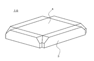
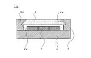
本実施形態に係る発光装置の外観構造について、図1、図2を用いて説明する。図1は、金属枠3と波長変換部材4のみを図示した要部斜視図であり、その他の部材については記載を省略している。図2は、本実施形態に係る発光装置の断面図である。
<Description of Structure FIGS. 1 to 3>
The external structure of the light emitting device according to this embodiment will be described with reference to FIGS. FIG. 1 is a perspective view of a main part illustrating only the
図1、図2に示す様に、本実施形態において波長変換部材4は、発光装置10の上面に配置されており、金属枠3によって周縁部を全て固定されている。基板2には、金属またはセラミック材料を主体として電極面が露出して形成されており、複数のLED素子1と図示しない電極面とが電気的に接合される。ここで、LED素子1の発光した際に発せられる熱は、基板2を経由して周囲へ放散する構成としているが、この構成に限定されず、例えば特許文献1記載の従来例、又はその他の記載しない従来例のようであってもよい。
As shown in FIGS. 1 and 2, in the present embodiment, the
金属枠3は、基板2の上に配置されており、複数のLED素子1を収容するように周囲を囲んでいる。金属枠3は、比較的容易に変形し可塑性が高く熱伝導性の優れた金属材料、例えばアルミニウムや銅のような素材より形成される。金属枠3は、内側領域に段差部3aを有し、この段差部3aの上面には、波長変換部材4の下面の周縁部が載置されている。
The
波長変換部材4は、透明な基材内に蛍光体が分散配置された平板状の部材である。その平面形状は本例では正方形であって厚板状である。基材の材質は、透光性、熱伝導性及び耐熱性の観点から、透光性樹脂よりも透光性セラミックスやガラス材より成ることが好ま
しい。この蛍光体は、青色光や紫外光を発するLED素子1の光によって励起され、LED素子1と異なる波長の光を発する。これにより、LED素子の光や、複数の蛍光体の色を混合させることで、例えば白色光化するなどLED素子1の本来の発光色と異なる演色効果を有することができる。
The
また、波長変換部4は、周縁端部に切欠部4aを備える。本実施形態にける切欠部4aは、図2に示すように波長変換部材4の側面が斜面形状となるように形成されている。この切欠部4aは、波長変換部材の上面と下面を除く4つ側面に形成されており、これらによって、波長変換部材4の形状は、下面から上面へ向かって断面積が漸減する錘台形状となっている。切欠部4aは、金属枠3の一部の金属に力を加えることで、その金属を塑性変形させ金属枠3の内側に突出して寄せられた変形部3dによってかしめ固定される。このようにして、金属枠3の段差部3aに波長変換部材4は固定される。
Moreover, the
また、金属枠3の金属が、波長変換部の切欠部4aのみをかしめて波長変換部材4の上面にまで金属が到達しないようにすることで、基板2の下面から波長変換部材4の上面までの高さと、基板2の下面から金属枠3の上面までの高さを略同一とすることができる。
Further, the metal of the
この様な構成とすることで、図3に示すように、下面が平面形状である前面透光性部材5を、金属枠3及び波長変換部材4の上面に配置する際に、金属枠3及び波長変換部材4と前面透光性部材5は密接して配置することができる。なお、本実施形態において前面透光性部材5に、下面が平面形状を有する凸レンズを用いたが、下面が平面形状の光学部材であれば、他の構成(板状部材を含むプリズム)を用いても良い。
With such a configuration, as shown in FIG. 3, when the front
<実施形態の作用>
波長変換部材4より発せられた励起熱は、熱伝導によって切欠部4aから金属枠3に接着剤などの樹脂を介さず直接伝わるため、効果的に外部に放熱される。また、金属枠3の上面と波長変換部材4の上面の高さが略同一となっていることから、金属枠3及び波長変換部材4上に、下面を平面形状とした、構造が単純な前面透光性部材5を、密接して配置することが可能となる。
<Operation of Embodiment>
Since the excitation heat generated from the
<実施形態の効果>
この様にして、本実施例の構成によれば、波長変換部材4より発せられた励起熱を、効果的に金属枠3へ放熱し、それにより、蛍光体の温度消光が減り、波長変換部材4の発光効率を高くすることができる。また、下面が平面形状である前面透光性部材5を、金属枠3及び波長変換部材4と密接して配置することによって、波長変換部材4から前面透光性部材5を経由し金属枠3へ至るという、新たな放熱経路を形成することができる。これにより、励起熱をさらに放熱できる為、波長変換部材4の発光効率は更に高くなる。また、前面透光性部材5が本実施形態のような凸レンズなどの光学部材であるならば、前面透光性部材の下面を単純な平面形状とできることから光学設計が容易となり、結果として所望の光学効果を得やすくなる。
<Effect of embodiment>
Thus, according to the configuration of the present embodiment, the excitation heat generated from the
次に、本実施形態に係る発光装置の製造方法について説明する。
発光装置の製造方法は、工程1:基板にLED素子と枠体を配置する工程、と、工程2:枠体段段差部に波長変換部材を載置する工程、と、工程3:波長変換部材をかしめ固定する工程、とによって構成される。このうち、工程1に関しては、従来知られているどのような方法を用いても良く、本発明の要部ではないため説明を省略する。以下、工程2、工程3より金属枠3に波長変換部材4をかしめ固定する具体的な製造方法について説明する。
Next, a method for manufacturing the light emitting device according to this embodiment will be described.
The manufacturing method of a light-emitting device includes: Step 1: a step of placing an LED element and a frame on a substrate; Step 2: a step of placing a wavelength conversion member on a step portion of the frame body; and Step 3: a wavelength conversion member. And caulking and fixing. Among these, regarding the
<工程2:枠体段段差部に波長変換部材を載置する工程 図4>
図4は、かしめ固定される前の金属枠13と波長変形部材4との配置関係を示す図で、(a)は斜視図、(b)は断面図である。かしめ固定される前の金属枠13は、その段差部3aの外側に直立部13bを備える。波長変換部材4は、その切欠部4aの斜面形状が上向きになるように、段差部3a上に落とし込んで載置される。段差部3aから直立部13bの上面までの高さは、波長変換部材4の上面までの高さよりも大きく設定されている。また各辺の直立部13bの上隅の部分は切欠部13cを設けて斜面状となし、金属枠3の4隅には金型係合部3eを設ける。
<Step 2: Step of Placing Wavelength Conversion Member on Frame Step Step> FIG.
4A and 4B are views showing the positional relationship between the
<金型 図5>
次に、かしめ固定を行うための金型について説明する。
図5は、かしめ固定される前の金属枠13の直立部13bをかしめて、図1〜図3に記載のように金属枠3に波長変換部材4を固定するために用いる金型の上型6の形態の一例を示す図である。(a)は上型6の下面の形状を見せるため上下を反転した下面側の斜視図、(b)は本来の向きにした上面側の斜視図である。6aは上面部、6bは側面部、6cは下面側の天井部、6dは突出部、6eは斜面部である。
<Mold Figure 5>
Next, a mold for performing caulking and fixing will be described.
FIG. 5 shows an upper mold of a mold used for fixing the
金型は、上型と下型から成る。下型は有底で直立する壁面を有する4角筒状をなし、プレス機に固定されているが図示していない。下型の筒状の内面は、かしめ固定される前の金属枠13の外側面及び上型の側面部6bに適合した寸法を有し、上型6は下型の内部で上下にスライドする。また、斜面部6eは図4に記載の金属枠3の切欠部13cに比べ、水平面に対する角度が浅く形成されている。
The mold consists of an upper mold and a lower mold. The lower mold is a quadrangular cylinder having a bottomed and upright wall surface, and is fixed to a press machine, but is not shown. The cylindrical inner surface of the lower mold has a size that fits the outer surface of the
<工程3:波長変換部材をかしめ固定する工程 図6>
図6は金属枠の変形前後の状態を上型と共に示す図であり、(a)は変形加工直前の状態斜視図、(b)はその断面図、(c)は変形加工完了後の斜視図、(d)はその断面図である。
このとき、図6(a)及び(b)においてかしめ固定される前の金属枠13は、波長変換部材4がかしめ固定される前の金属枠13の段差部3aに載置された状態で、図示しない下型の底部に置かれている。
このとき、角筒状の下型は、金属枠3の直立部3bの金属がかしめ固定される前の金属枠13の内側へのみに流れ、外側へ向かいはみ出すことを防止している。その図示はしないが、作用は自明である。
<Step 3: Step of Caulking and Fixing Wavelength Conversion Member FIG. 6>
6A and 6B are views showing the state before and after the deformation of the metal frame together with the upper mold. FIG. 6A is a perspective view of the state immediately before the deformation process, FIG. 6B is a cross-sectional view thereof, and FIG. , (D) is a sectional view thereof.
At this time, the
At this time, the lower mold of the rectangular tube shape prevents the metal of the upright portion 3b of the
図6(a)及び(b)において、上型6の天井部6cは平面形状を有し、かしめ固定される前の金属枠13の直立部13bの上面に載っている。上述のとおり直立部13bの上面が波長変換部材の上面より高いので、波長変換部材4の上面と天井部6cの間には所定量だけ隙間が生じている。また、突出部6dの突端側はかしめ固定される前の金属枠13の金型係合部13eと一部係合している。
6 (a) and 6 (b), the ceiling portion 6c of the
図6(c)及び(d)において、上型6の上面部6aが図示しないプレス機に押圧されて、上型6の突出部6dの先端がかしめ固定される前の金属枠13を載置した下型の底面に当接するまで上型6を沈下する。このとき、図6(b)の直立部における波長変換部材より上の金属の量などを調整することで上型6の下面側の天井部6cは、波長変換部材4の上面と当接させることができる。すなわち、図6(a)に記載の直立部13bは天井部6cに潰されて金属枠の内側へ突出して変形部3dとなり、波長変換部材4の切欠部4aのみがかしめ固定され、波金属枠3の上面と波長変換部材4の上面の高さを同一とすることができる。
6 (c) and 6 (d), the
その際、突出部6dを有することによって過剰な押圧を防ぐことができる。
また、上述のとおり、上型6は斜面部6eとかしめ固定される前の金属枠13の切欠部
13cが共に傾斜面を有し、斜面部6eは切欠部13cに比べて水平面に対する角度が浅く形成されている。これにより、傾斜部6eと切欠部13cが共にガイドの役割をすることで近くに金属の少ない波長変換部材4の角部も綺麗にかしめ固定することが可能となる。
なお、金型の上型6を下げきった際に、金属が波長変換部材4の上面に乗り上げず、また、不要なすきまができないように、かしめ固定される前の金属枠13の直立部13bの高さ、切欠部13cの形状・寸法、上型6の突出部6d、その斜面部6eの形状・寸法が設定されるのは勿論である。このようにして、波長変換部材4のかしめ固定が終了する。
At this time, excessive pressing can be prevented by having the protrusion 6d.
In addition, as described above, the
In addition, when the
<他の実施形態について>
本実施形態において、波長変換部材4の切欠部4aを斜面形状としたが、斜面形状に代えて段差(階段)形状として切欠部4を形成してもよい。ただし、段差形状よりも斜面形状の方がよりスムーズに金属を塑性変形させることができるため、かしめ固定をよりきれいにおこなうことができる。
<About other embodiments>
In the present embodiment, the cutout portion 4a of the
また、本実施形態において、波長変換部材4の上面は正方形としたが、これに限らず、長方形、または円形であっても良い。また、波長変換部材4の形状に合わせて金属枠3の形状も任意に変更してよい。
また、本実施形態において波長変換部材4の4辺を全てかしめ固定しているが、これに限らず例えば向かい合う2辺のみを固定するなど、一部だけを固定してもよい。
また、本実施形態において、前面透光性部材5を凸レンズとしたが、これに限らず例えば他のレンズ、プリズムなどの光学部材や、光学的な機能を有さない透明な熱伝導部材であってもよい。
In the present embodiment, the upper surface of the
In the present embodiment, all four sides of the
In the present embodiment, the front
また、本実施形態において、LED素子1は複数として説明したが、個数に限定はなく、1個でもよい。
さらに、LED素子の実装方法としては、特に限定はなく、基板上へのフリップチップ実装や、ダイボンド実装した後に電極面とLED素子の電極をワイヤーボンディングにて接合してもよい。
In the present embodiment, a plurality of
Furthermore, the mounting method of the LED element is not particularly limited, and the electrode surface and the electrode of the LED element may be joined by wire bonding after flip chip mounting on the substrate or die bonding mounting.
その他、各部材の材質、形状に種々の変更を与えることが考えられる。なお、LED素子以外の発光素子を用いて発光装置を構成してもよい。 In addition, it is possible to give various changes to the material and shape of each member. In addition, you may comprise a light-emitting device using light emitting elements other than an LED element.
1 LED素子
2 基板
3 金属枠
3a 段差部
3d 変形部
4 波長変換部材
4a 切欠部
5 前面透光性部材
6 金型
6a 上面部
6b 側面部
6c 天井部
6d 突出部
6e 斜面部
10 発光装置
13 かしめ固定される前の金属枠
13b 直立部
13c 切欠部
13e 金型係合部
DESCRIPTION OF
Claims (4)
前記LED素子を取り囲むように配置された金属枠体と、
前記金属枠体の内側に形成された段差部と、
該段差部に配置された平板上の波長変換部材と、を備え、
前記波長変換部材は、上面端部に切欠部を有し、
前記金属枠体は、前記切欠部に対応した箇所に突出部を有し、
前記基板の下面から前記波長変換部材の上面までの高さと、前記基板の下面から前記金属枠体の上面までの高さが同一となるように、前記突出部によってかしめ固定されてなることを特徴とする発光装置。 An LED element mounted on a substrate;
A metal frame disposed so as to surround the LED element;
A step portion formed inside the metal frame;
A wavelength conversion member on a flat plate disposed in the step portion,
The wavelength conversion member has a notch at the upper surface end,
The metal frame has a protrusion at a location corresponding to the notch,
The protrusion is caulked and fixed so that the height from the lower surface of the substrate to the upper surface of the wavelength conversion member is the same as the height from the lower surface of the substrate to the upper surface of the metal frame. A light emitting device.
Priority Applications (1)
| Application Number | Priority Date | Filing Date | Title |
|---|---|---|---|
| JP2016062948A JP6754206B2 (en) | 2016-03-28 | 2016-03-28 | Light emitting device |
Applications Claiming Priority (1)
| Application Number | Priority Date | Filing Date | Title |
|---|---|---|---|
| JP2016062948A JP6754206B2 (en) | 2016-03-28 | 2016-03-28 | Light emitting device |
Publications (2)
| Publication Number | Publication Date |
|---|---|
| JP2017183302A true JP2017183302A (en) | 2017-10-05 |
| JP6754206B2 JP6754206B2 (en) | 2020-09-09 |
Family
ID=60007134
Family Applications (1)
| Application Number | Title | Priority Date | Filing Date |
|---|---|---|---|
| JP2016062948A Active JP6754206B2 (en) | 2016-03-28 | 2016-03-28 | Light emitting device |
Country Status (1)
| Country | Link |
|---|---|
| JP (1) | JP6754206B2 (en) |
Cited By (3)
| Publication number | Priority date | Publication date | Assignee | Title |
|---|---|---|---|---|
| JP2019086778A (en) * | 2017-11-09 | 2019-06-06 | 日本特殊陶業株式会社 | Optical wavelength conversion component, light-emitting device, and method for manufacturing optical wavelength conversion component |
| JP2019086777A (en) * | 2017-11-09 | 2019-06-06 | 日本特殊陶業株式会社 | Optical wavelength conversion component, light-emitting device, and method for manufacturing optical wavelength conversion component |
| WO2021085458A1 (en) * | 2019-10-30 | 2021-05-06 | 京セラ株式会社 | Light-emitting element mounting package and light-emitting device |
Citations (6)
| Publication number | Priority date | Publication date | Assignee | Title |
|---|---|---|---|---|
| JPH1090578A (en) * | 1996-09-17 | 1998-04-10 | Minolta Co Ltd | Lens device and lens assembling method |
| JPH10233532A (en) * | 1997-02-21 | 1998-09-02 | Houshin Kagaku Sangiyoushiyo:Kk | Light emitting diode |
| JP2006013426A (en) * | 2004-01-28 | 2006-01-12 | Kyocera Corp | Light emitting device and lighting apparatus |
| JP2007173397A (en) * | 2005-12-20 | 2007-07-05 | Matsushita Electric Ind Co Ltd | LIGHT EMITTING MODULE AND DISPLAY DEVICE AND LIGHTING DEVICE USING THE SAME |
| JP2010272847A (en) * | 2009-04-20 | 2010-12-02 | Nichia Corp | Light emitting device |
| US20120305970A1 (en) * | 2011-06-02 | 2012-12-06 | Hyung Kun Kim | Light emitting device package and manufacturing method thereof |
-
2016
- 2016-03-28 JP JP2016062948A patent/JP6754206B2/en active Active
Patent Citations (6)
| Publication number | Priority date | Publication date | Assignee | Title |
|---|---|---|---|---|
| JPH1090578A (en) * | 1996-09-17 | 1998-04-10 | Minolta Co Ltd | Lens device and lens assembling method |
| JPH10233532A (en) * | 1997-02-21 | 1998-09-02 | Houshin Kagaku Sangiyoushiyo:Kk | Light emitting diode |
| JP2006013426A (en) * | 2004-01-28 | 2006-01-12 | Kyocera Corp | Light emitting device and lighting apparatus |
| JP2007173397A (en) * | 2005-12-20 | 2007-07-05 | Matsushita Electric Ind Co Ltd | LIGHT EMITTING MODULE AND DISPLAY DEVICE AND LIGHTING DEVICE USING THE SAME |
| JP2010272847A (en) * | 2009-04-20 | 2010-12-02 | Nichia Corp | Light emitting device |
| US20120305970A1 (en) * | 2011-06-02 | 2012-12-06 | Hyung Kun Kim | Light emitting device package and manufacturing method thereof |
Cited By (5)
| Publication number | Priority date | Publication date | Assignee | Title |
|---|---|---|---|---|
| JP2019086778A (en) * | 2017-11-09 | 2019-06-06 | 日本特殊陶業株式会社 | Optical wavelength conversion component, light-emitting device, and method for manufacturing optical wavelength conversion component |
| JP2019086777A (en) * | 2017-11-09 | 2019-06-06 | 日本特殊陶業株式会社 | Optical wavelength conversion component, light-emitting device, and method for manufacturing optical wavelength conversion component |
| JP7188984B2 (en) | 2017-11-09 | 2022-12-13 | 日本特殊陶業株式会社 | Method for manufacturing optical wavelength conversion component |
| JP7221653B2 (en) | 2017-11-09 | 2023-02-14 | 日本特殊陶業株式会社 | Method for manufacturing optical wavelength conversion component and light emitting device |
| WO2021085458A1 (en) * | 2019-10-30 | 2021-05-06 | 京セラ株式会社 | Light-emitting element mounting package and light-emitting device |
Also Published As
| Publication number | Publication date |
|---|---|
| JP6754206B2 (en) | 2020-09-09 |
Similar Documents
| Publication | Publication Date | Title |
|---|---|---|
| US7872273B2 (en) | Light emitting device | |
| JP3138795U (en) | Semiconductor light emitting device and planar light source using semiconductor light emitting device | |
| JP2010003743A (en) | Light-emitting device | |
| JP2008282932A (en) | Light emitting device and manufacturing method thereof | |
| JP2013115116A (en) | Led module | |
| JP2011187963A (en) | Light emitting element package, display device including the same, and lighting system | |
| US8569080B2 (en) | Method for packaging light emitting diode | |
| JP2017183302A (en) | Light emitting device | |
| US9059384B2 (en) | LED packaging construction and manufacturing method thereof | |
| JP2005116937A (en) | Semiconductor light emitting device and manufacturing method thereof | |
| CN102082223B (en) | Light emitting device package | |
| KR20080079745A (en) | Light emitting diode package base having double heat dissipation structure between lead frame and heat dissipation plate and manufacturing method | |
| US7508008B2 (en) | Light-emitting device | |
| CN102479911B (en) | Light emitting device package | |
| JP2017050108A (en) | Light emitting device | |
| KR20100036892A (en) | Light emitting diode package | |
| KR20110013401A (en) | LED package, lead frame and its manufacturing method | |
| JP4967347B2 (en) | Manufacturing method of linear light source and semiconductor light emitting unit | |
| JP2017059756A (en) | Light-emitting device | |
| JP4679917B2 (en) | Semiconductor light emitting device | |
| TW201403870A (en) | Light emitting diode element and manufacturing mathod thereof | |
| JP2017050356A (en) | Manufacturing method for light-emitting device | |
| JP2017050345A (en) | Method for manufacturing light emitting device | |
| JP2013187269A (en) | Optical semiconductor device and manufacturing method of the same | |
| TWI553384B (en) | Back light |
Legal Events
| Date | Code | Title | Description |
|---|---|---|---|
| A621 | Written request for application examination |
Free format text: JAPANESE INTERMEDIATE CODE: A621 Effective date: 20181101 |
|
| A977 | Report on retrieval |
Free format text: JAPANESE INTERMEDIATE CODE: A971007 Effective date: 20190911 |
|
| A131 | Notification of reasons for refusal |
Free format text: JAPANESE INTERMEDIATE CODE: A131 Effective date: 20191029 |
|
| A521 | Request for written amendment filed |
Free format text: JAPANESE INTERMEDIATE CODE: A523 Effective date: 20191225 |
|
| RD02 | Notification of acceptance of power of attorney |
Free format text: JAPANESE INTERMEDIATE CODE: A7422 Effective date: 20200225 |
|
| RD03 | Notification of appointment of power of attorney |
Free format text: JAPANESE INTERMEDIATE CODE: A7423 Effective date: 20200303 |
|
| RD04 | Notification of resignation of power of attorney |
Free format text: JAPANESE INTERMEDIATE CODE: A7424 Effective date: 20200311 |
|
| A131 | Notification of reasons for refusal |
Free format text: JAPANESE INTERMEDIATE CODE: A131 Effective date: 20200602 |
|
| A521 | Request for written amendment filed |
Free format text: JAPANESE INTERMEDIATE CODE: A523 Effective date: 20200710 |
|
| TRDD | Decision of grant or rejection written | ||
| A01 | Written decision to grant a patent or to grant a registration (utility model) |
Free format text: JAPANESE INTERMEDIATE CODE: A01 Effective date: 20200804 |
|
| A61 | First payment of annual fees (during grant procedure) |
Free format text: JAPANESE INTERMEDIATE CODE: A61 Effective date: 20200821 |
|
| R150 | Certificate of patent or registration of utility model |
Ref document number: 6754206 Country of ref document: JP Free format text: JAPANESE INTERMEDIATE CODE: R150 |
|
| R250 | Receipt of annual fees |
Free format text: JAPANESE INTERMEDIATE CODE: R250 |
|
| R250 | Receipt of annual fees |
Free format text: JAPANESE INTERMEDIATE CODE: R250 |