JP2017183459A - Copper foil, copper clad laminate sheet, flexible printed circuit board and electronic apparatus - Google Patents
Copper foil, copper clad laminate sheet, flexible printed circuit board and electronic apparatus Download PDFInfo
- Publication number
- JP2017183459A JP2017183459A JP2016067413A JP2016067413A JP2017183459A JP 2017183459 A JP2017183459 A JP 2017183459A JP 2016067413 A JP2016067413 A JP 2016067413A JP 2016067413 A JP2016067413 A JP 2016067413A JP 2017183459 A JP2017183459 A JP 2017183459A
- Authority
- JP
- Japan
- Prior art keywords
- copper foil
- curve
- copper
- roughness
- clad laminate
- Prior art date
- Legal status (The legal status is an assumption and is not a legal conclusion. Google has not performed a legal analysis and makes no representation as to the accuracy of the status listed.)
- Granted
Links
Images
Classifications
-
- B—PERFORMING OPERATIONS; TRANSPORTING
- B32—LAYERED PRODUCTS
- B32B—LAYERED PRODUCTS, i.e. PRODUCTS BUILT-UP OF STRATA OF FLAT OR NON-FLAT, e.g. CELLULAR OR HONEYCOMB, FORM
- B32B15/00—Layered products comprising a layer of metal
- B32B15/20—Layered products comprising a layer of metal comprising aluminium or copper
-
- H—ELECTRICITY
- H05—ELECTRIC TECHNIQUES NOT OTHERWISE PROVIDED FOR
- H05K—PRINTED CIRCUITS; CASINGS OR CONSTRUCTIONAL DETAILS OF ELECTRIC APPARATUS; MANUFACTURE OF ASSEMBLAGES OF ELECTRICAL COMPONENTS
- H05K1/00—Printed circuits
- H05K1/02—Details
- H05K1/0277—Bendability or stretchability details
- H05K1/0283—Stretchable printed circuits
-
- B—PERFORMING OPERATIONS; TRANSPORTING
- B32—LAYERED PRODUCTS
- B32B—LAYERED PRODUCTS, i.e. PRODUCTS BUILT-UP OF STRATA OF FLAT OR NON-FLAT, e.g. CELLULAR OR HONEYCOMB, FORM
- B32B15/00—Layered products comprising a layer of metal
- B32B15/04—Layered products comprising a layer of metal comprising metal as the main or only constituent of a layer, which is next to another layer of the same or of a different material
- B32B15/08—Layered products comprising a layer of metal comprising metal as the main or only constituent of a layer, which is next to another layer of the same or of a different material of synthetic resin
-
- H—ELECTRICITY
- H05—ELECTRIC TECHNIQUES NOT OTHERWISE PROVIDED FOR
- H05K—PRINTED CIRCUITS; CASINGS OR CONSTRUCTIONAL DETAILS OF ELECTRIC APPARATUS; MANUFACTURE OF ASSEMBLAGES OF ELECTRICAL COMPONENTS
- H05K1/00—Printed circuits
- H05K1/02—Details
- H05K1/0296—Conductive pattern lay-out details not covered by sub groups H05K1/02 - H05K1/0295
- H05K1/0298—Multilayer circuits
-
- H—ELECTRICITY
- H05—ELECTRIC TECHNIQUES NOT OTHERWISE PROVIDED FOR
- H05K—PRINTED CIRCUITS; CASINGS OR CONSTRUCTIONAL DETAILS OF ELECTRIC APPARATUS; MANUFACTURE OF ASSEMBLAGES OF ELECTRICAL COMPONENTS
- H05K1/00—Printed circuits
- H05K1/02—Details
- H05K1/09—Use of materials for the conductive, e.g. metallic pattern
-
- H—ELECTRICITY
- H05—ELECTRIC TECHNIQUES NOT OTHERWISE PROVIDED FOR
- H05K—PRINTED CIRCUITS; CASINGS OR CONSTRUCTIONAL DETAILS OF ELECTRIC APPARATUS; MANUFACTURE OF ASSEMBLAGES OF ELECTRICAL COMPONENTS
- H05K3/00—Apparatus or processes for manufacturing printed circuits
- H05K3/46—Manufacturing multilayer circuits
- H05K3/4611—Manufacturing multilayer circuits by laminating two or more circuit boards
-
- B—PERFORMING OPERATIONS; TRANSPORTING
- B32—LAYERED PRODUCTS
- B32B—LAYERED PRODUCTS, i.e. PRODUCTS BUILT-UP OF STRATA OF FLAT OR NON-FLAT, e.g. CELLULAR OR HONEYCOMB, FORM
- B32B2311/00—Metals, their alloys or their compounds
- B32B2311/12—Copper
-
- B—PERFORMING OPERATIONS; TRANSPORTING
- B32—LAYERED PRODUCTS
- B32B—LAYERED PRODUCTS, i.e. PRODUCTS BUILT-UP OF STRATA OF FLAT OR NON-FLAT, e.g. CELLULAR OR HONEYCOMB, FORM
- B32B2457/00—Electrical equipment
- B32B2457/08—PCBs, i.e. printed circuit boards
-
- H—ELECTRICITY
- H05—ELECTRIC TECHNIQUES NOT OTHERWISE PROVIDED FOR
- H05K—PRINTED CIRCUITS; CASINGS OR CONSTRUCTIONAL DETAILS OF ELECTRIC APPARATUS; MANUFACTURE OF ASSEMBLAGES OF ELECTRICAL COMPONENTS
- H05K2201/00—Indexing scheme relating to printed circuits covered by H05K1/00
- H05K2201/03—Conductive materials
- H05K2201/0332—Structure of the conductor
- H05K2201/0335—Layered conductors or foils
- H05K2201/0355—Metal foils
-
- H—ELECTRICITY
- H05—ELECTRIC TECHNIQUES NOT OTHERWISE PROVIDED FOR
- H05K—PRINTED CIRCUITS; CASINGS OR CONSTRUCTIONAL DETAILS OF ELECTRIC APPARATUS; MANUFACTURE OF ASSEMBLAGES OF ELECTRICAL COMPONENTS
- H05K2203/00—Indexing scheme relating to apparatus or processes for manufacturing printed circuits covered by H05K3/00
- H05K2203/06—Lamination
Landscapes
- Engineering & Computer Science (AREA)
- Microelectronics & Electronic Packaging (AREA)
- Manufacturing & Machinery (AREA)
- Laminated Bodies (AREA)
- Parts Printed On Printed Circuit Boards (AREA)
- Metal Rolling (AREA)
- Reduction Rolling/Reduction Stand/Operation Of Reduction Machine (AREA)
Abstract
【課題】自身の厚みが薄くても樹脂層とのラミネート時にシワが発生し難い銅箔、銅張積層板、並びにフレキシブルプリント基板及び電子機器を提供する。【解決手段】質量率で99.90%以上の銅を含む厚み3〜8μmの銅箔であって、JIS-B0601(2013)に従い、TD方向に沿う50mmの長さLの表面2の断面曲線Sから、輪郭曲線フィルタλc=2 mm,輪郭曲線フィルタλf=25mmの条件で短波長及び長波長成分をカットオフしてうねり曲線を求めたとき、うねり曲線要素の平均長さWsmが2.5〜20.0mmである。【選択図】図2Provided are a copper foil, a copper clad laminate, a flexible printed board, and an electronic device that are less likely to be wrinkled when laminated with a resin layer even if the thickness of the film is thin. SOLUTION: A copper foil having a thickness of 3 to 8 μm containing 99.90% or more of copper by mass, according to JIS-B0601 (2013), from a cross-sectional curve S of a surface 2 having a length L of 50 mm along the TD direction. When the undulation curve is obtained by cutting off the short wavelength and long wavelength components under the conditions of the outline curve filter λc = 2 mm and the outline curve filter λf = 25 mm, the average length Wsm of the undulation curve element is 2.5 to 20.0 mm. is there. [Selection] Figure 2
Description
本発明は、ラミネート方式およびキャスト方式で製造される銅張積層板に好適に用いられる銅箔、それを用いた銅張積層板、並びにフレキシブルプリント基板及び電子機器に関する。 The present invention relates to a copper foil suitably used for a copper clad laminate manufactured by a laminate method and a cast method, a copper clad laminate using the copper foil, a flexible printed board, and an electronic device.
電子機器に使用されるフレキシブル配線板(FPC)は、銅箔と樹脂とを積層して銅張積層板(CCL)を製造し、このCCLの銅箔部分に回路を形成してなる。CCLの製法としては、熱可塑性樹脂を有する樹脂フィルムと銅箔とを熱融着するラミネート法(特許文献1)、樹脂ワニスを銅箔に塗工して樹脂を硬化させるキャスト法(特許文献2)、ダブルベルトプレス法(特許文献3)などがある。 A flexible wiring board (FPC) used for electronic equipment is made by laminating a copper foil and a resin to produce a copper clad laminate (CCL), and forming a circuit on the copper foil portion of the CCL. As a method for producing CCL, a laminating method (Patent Document 1) in which a resin film having a thermoplastic resin and a copper foil are heat-sealed, and a casting method (Patent Document 2) in which a resin varnish is applied to the copper foil and the resin is cured. ) And double belt press method (Patent Document 3).
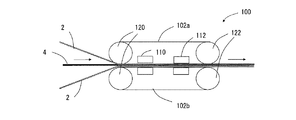
ダブルベルトプレス法は、図1に示すダブルベルトプレス装置100を用いる。、ダブルベルトプレス装置100は、継ぎ目なしのスチールベルト102a、102bを2つ用意し、それぞれのベルト102a、102bをそれぞれ入口ロール120及び出口ロール122間に掛架する。
そして、各ベルト102a、102bを密接させて走行させると、入口ロール120側の銅箔2及び樹脂フィルム4が各ベルト102a、102b間に引き込まれ、各ベルト102a、102bで積層及び熱プレスされて出口ロール122側から出るようになる。
各ベルト102a、102b間に加熱加圧装置110、冷却加圧装置112を配置することで、銅箔2及び樹脂フィルム4を熱圧着してCCLを製造できる。
The double belt press method uses a double
When the
By disposing the heating and pressing
近年、フレキシブル配線板においてファインピッチ化,薄型化が要求されるようになっている。すなわち、当該用途に基板として用いる銅張積層板(CCL)基板や、銅張積層板に用いられる銅箔にもこれまで以上に薄肉化が求められることになる。 In recent years, there has been a demand for fine pitch and thinning of flexible wiring boards. That is, the copper-clad laminate (CCL) substrate used as a substrate for the application and the copper foil used for the copper-clad laminate are required to be thinner than ever.
ところで、銅張積層板は、銅箔の厚みが薄くなると、樹脂と積層するときにシワが入りやすく、生産性や歩留りの低下を招く。
特に、銅箔上に樹脂ワニスを塗工する形成するキャスト法では、銅箔にシワが入ると製造は困難になる。又、ラミネート法ではヒートロールを用いて熱融着を行うが、ロール間の銅箔に張力を掛けると、張力方向と平行にシワが入り易い。
By the way, when the thickness of the copper clad laminate is reduced, the copper clad laminate is likely to be wrinkled when it is laminated with the resin, resulting in a decrease in productivity and yield.
In particular, in the casting method in which a resin varnish is applied on a copper foil, the production becomes difficult if wrinkles enter the copper foil. In the laminating method, heat fusion is performed using a heat roll. However, when tension is applied to the copper foil between the rolls, wrinkles are likely to be generated in parallel with the tension direction.
従って、本発明の目的は、自身の厚みが薄くても樹脂層と積層させるときにシワが発生し難い銅箔、銅張積層板、並びにフレキシブルプリント基板及び電子機器を提供することにある。 Accordingly, an object of the present invention is to provide a copper foil, a copper clad laminate, a flexible printed circuit board, and an electronic device that are less likely to be wrinkled when laminated with a resin layer even if the thickness of the film is thin.
本発明者らは、厚みが薄い銅箔を樹脂層と積層してCCLを製造した際にシワが発生する原因が、銅箔の表面性状に相関があることを見出した。
銅箔の表面性状として、粗さ計による表面の高さプロファイル(断面曲線)が挙げられるが、銅箔では一般に0.1〜5mm程度の長さの表面の断面曲線を求め、断面曲線から表面粗さ等の指標を求めている。
ところが、本発明者らが検討した結果、長い距離の銅箔表面の断面曲線から求めた表面性状(うねり曲線)が、樹脂と張り合わせるときに入るシワと大きな相関があることが判明した。
The present inventors have found that the cause of wrinkling when a thin copper foil is laminated with a resin layer to produce CCL is correlated with the surface properties of the copper foil.
The surface properties of copper foil include the surface height profile (cross-sectional curve) measured by a roughness meter. In general, the copper foil calculates the cross-sectional curve of the surface with a length of about 0.1 to 5 mm, and the surface roughness from the cross-sectional curve. Etc. are being sought.
However, as a result of investigations by the present inventors, it has been found that the surface texture (waviness curve) obtained from the cross-sectional curve of the copper foil surface over a long distance has a large correlation with wrinkles entering when the resin is laminated.
すなわち、本発明の圧延銅箔は、質量率で99.90%以上の銅を含む厚み3〜8μmの銅箔であって、JIS-B0601(2013)に従い、TD方向に沿う50mmの長さの表面の断面曲線から、輪郭曲線フィルタλc=2 mm,輪郭曲線フィルタλf=25mmの条件で短波長及び長波長成分をカットオフしてうねり曲線を求めたとき、うねり曲線要素の平均長さWsmが2.5〜20.0mmであることを特徴とする。 That is, the rolled copper foil of the present invention is a copper foil having a thickness of 3 to 8 μm containing 99.90% or more of copper by mass, and has a surface with a length of 50 mm along the TD direction according to JIS-B0601 (2013). When the undulation curve is obtained by cutting off the short wavelength and long wavelength components under the conditions of the outline curve filter λc = 2 mm and the outline curve filter λf = 25 mm from the cross-section curve, the average length Wsm of the undulation curve element is 2.5 to It is 20.0 mm.
前記うねり曲線の最大高さうねりWzが0.00010〜0.00200mmであることが好ましい。
本発明の圧延銅箔は、圧延銅箔であってAg,Zn,Sn及びPの群から選ばれる1種以上の添加元素を合計で10〜2000質量ppm含有することが好ましい。
片面又は両面にCu,Ni,Zn及びCoの群から選ばれる1種以上の元素からなるめっき層が形成されていることが好ましい。
前記断面曲線から、λc=0.25mmで長波長成分をカットオフして粗さ曲線を求めたとき、、該粗さ曲線から計算される算術平均粗さRaが0.01〜0.1μmであり、最大高さ粗さRzが0.1〜0.8μmであることが好ましい。
The maximum height waviness Wz of the waviness curve is preferably 0.00010 to 0.00200 mm.
The rolled copper foil of the present invention is a rolled copper foil and preferably contains 10 to 2000 mass ppm of one or more additive elements selected from the group consisting of Ag, Zn, Sn and P in total.
It is preferable that the plating layer which consists of 1 or more types of elements chosen from the group of Cu, Ni, Zn, and Co is formed in the single side | surface or both surfaces.
When the roughness curve is obtained by cutting off the long wavelength component at λc = 0.25 mm from the cross-sectional curve, the arithmetic average roughness Ra calculated from the roughness curve is 0.01 to 0.1 μm, and the maximum height The roughness Rz is preferably 0.1 to 0.8 μm.
本発明の銅張積層板は、前記の銅箔と、樹脂層とで構成される。 The copper clad laminate of the present invention is composed of the copper foil and the resin layer.
本発明のフレキシブルプリント基板は、前記銅張積層板を用い、前記銅箔に回路を形成してなる。 The flexible printed board of the present invention is formed by using the copper-clad laminate and forming a circuit on the copper foil.
本発明の電子機器は、前記フレキシブルプリント基板を用いてなる。 The electronic device of the present invention uses the flexible printed circuit board.
本発明によれば、自身の厚みが薄くても樹脂層とのラミネート時にシワが発生し難い銅箔を得ることができる。 According to the present invention, it is possible to obtain a copper foil that is less likely to be wrinkled at the time of lamination with a resin layer even if its own thickness is small.
以下、本発明の実施形態に係る圧延銅箔について説明する。なお、本発明において%とは、特に断らない限り、質量%を示すものとする。本発明の実施形態に係る圧延銅箔は、樹脂フィルム等の樹脂層とラミネート処理されて製造される銅張積層板に有用であるが、上述のキャスト法、ダブルベルト法にも適用できる。 Hereinafter, the rolled copper foil which concerns on embodiment of this invention is demonstrated. In the present invention, “%” means “% by mass” unless otherwise specified. Although the rolled copper foil which concerns on embodiment of this invention is useful for the copper clad laminated board manufactured by laminating with resin layers, such as a resin film, it is applicable also to the above-mentioned casting method and a double belt method.
<組成>
圧延銅箔は質量率で99.90%以上の銅を含む。このような組成としては、JIS-H3100(C1100)に規格されるタフピッチ銅、又はJIS- H3100 (C1020)に規格される無酸素銅が挙げられる。圧延銅箔が質量率で銅を99.90〜99.999% 、酸素を0〜500質量ppmの範囲で含有すると好ましい。
<Composition>
The rolled copper foil contains 99.90% or more copper by mass. Examples of such a composition include tough pitch copper specified by JIS-H3100 (C1100) or oxygen-free copper specified by JIS-H3100 (C1020). It is preferable that the rolled copper foil contains 99.90 to 99.999% copper and oxygen in the range of 0 to 500 ppm by mass in terms of mass ratio.
さらに、上記したタフピッチ銅又は無酸素銅に対し、Ag,Zn,Sn及びPの群から選ばれる1種以上の添加元素を合計で10〜2000質量ppm含有してもよい。これらの添加元素を加えることで、折り曲げ性や屈曲性を向上させる{100}方位の割合が増える。
上記元素の合計量が10質量ppm未満であると、銅箔の屈曲性が低下することがあり、上記元素の合計量が2000質量ppmを超えると導電率の低下が著しくなることがある。
特に、これらの添加元素を10〜500質量ppm含有させると折り曲げ性や屈曲性をさらに向上できる。又、これらの添加元素を500〜2000質量ppm含有させると硬くなり、CCL製造時にシワがより入り難くなる。
Furthermore, you may contain 10-2000 mass ppm in total with 1 or more types of additional elements chosen from the group of Ag, Zn, Sn, and P with respect to the above-mentioned tough pitch copper or oxygen-free copper. By adding these additive elements, the ratio of the {100} orientation that improves bendability and bendability increases.
If the total amount of the above elements is less than 10 ppm by mass, the flexibility of the copper foil may be lowered, and if the total amount of the above elements exceeds 2000 ppm by mass, the conductivity may be significantly reduced.
In particular, when these additive elements are contained in an amount of 10 to 500 ppm by mass, the bendability and bendability can be further improved. In addition, when these additive elements are contained in an amount of 500 to 2000 ppm by mass, it becomes hard and wrinkles are more difficult to enter during CCL production.
<厚み>
銅箔の厚みは3〜8μmとする。厚さ3μm未満の銅箔は製造が困難である。又、銅箔の厚みが8μmを超えるものは、本発明で課題とするシワが生じ難いので、対象外とする。
<Thickness>
The thickness of the copper foil is 3 to 8 μm. A copper foil having a thickness of less than 3 μm is difficult to manufacture. Moreover, since the wrinkle made into a subject with this invention does not produce easily when the thickness of copper foil exceeds 8 micrometers, it excludes it from object.
<めっき層>
銅箔の片面又は両面に、Cu,Ni,Zn及びCoの群から選ばれる1種以上の元素からなるめっき層が形成されていてもよい。
これらのめっき層は、樹脂と積層してCCLを製造する際、樹脂との密着性を向上させるものであり、通常、粗化めっき層とする。
<Plating layer>
A plating layer made of one or more elements selected from the group consisting of Cu, Ni, Zn, and Co may be formed on one side or both sides of the copper foil.
When these plating layers are laminated with a resin to produce CCL, the adhesion with the resin is improved and is usually a roughened plating layer.
<銅箔の表面性状>
JIS-B0601(2013)に従い、TD方向に沿う50mmの長さの表面の断面曲線から、輪郭曲線フィルタλc=2 mm,輪郭曲線フィルタλf=25mmの条件で短波長及び長波長成分をカットオフしてうねり曲線を求めたとき、うねり曲線要素の平均長さWsmが2.5〜20.0mmである。
ここで、TD(Transverse Direction)方向は、MD方向(Machine Directionm)と直角な方向である。圧延銅箔の場合、TD方向は圧延直角方向である。
<Surface properties of copper foil>
In accordance with JIS-B0601 (2013), the short wavelength and long wavelength components are cut off from the cross-sectional curve of the surface with a length of 50 mm along the TD direction under the conditions of contour curve filter λc = 2 mm and contour curve filter λf = 25 mm. When the waviness curve is obtained, the average length Wsm of the waviness curve element is 2.5 to 20.0 mm.
Here, the TD (Transverse Direction) direction is a direction perpendicular to the MD direction (Machine Directionm). In the case of rolled copper foil, the TD direction is the direction perpendicular to the rolling.
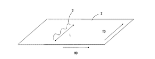
そして、図2に示すように、銅箔2の表面のTD方向に沿う50mmの長さLに沿って、高さプロファイルを示す断面曲線Sを測定する。なお、銅箔の片面に上述のめっき層が形成されている場合、めっきされていない銅箔表面の断面曲線Sを測定する。銅箔の両面に上述のめっき層が形成されている場合、まず、両方のめっき層表面につき、後述の方法で算術平均粗さRaを測定し、Raの小さい方の面の断面曲線Sを測定する。
Then, as shown in FIG. 2, a cross-sectional curve S indicating a height profile is measured along a length L of 50 mm along the TD direction of the surface of the
断面曲線は、JIS-B0601-2013「3.1.5」に記載の「断面曲線(primary profile)」である。
次に、「うねり曲線」は以下のようにして求める。まず、断面曲線からλ輪郭曲線フィルタc:2mm(但し、λcはJIS-B0601-2013「3.1.1.2」に記載の「粗さ成分とうねり成分との境界を定義するフィルタ」)より短波長の表面粗さの成分を低域フィルタによって除去する。さらに、この曲線から輪郭曲線フィルタλf:25mm(但し、λfはJIS-B0601-2013「3.1.1.3」に記載の「うねり成分とそれより長い波長成分との境界を定義するフィルタ」)より長波長の表面粗さの成分を高域フィルタによって除去し、うねり曲線が得られる。
The cross-sectional curve is a “primary profile” described in JIS-B0601-2013 “3.1.5”.
Next, the “waviness curve” is obtained as follows. First, from the cross-sectional curve, λ contour curve filter c: 2 mm (where λc is a “filter that defines the boundary between roughness component and waviness component” described in JIS-B0601-2013 “3.1.1.2”). The surface roughness component is removed by a low-pass filter. Furthermore, from this curve, the contour curve filter λf: 25 mm (where λf is the “filter that defines the boundary between the swell component and the longer wavelength component” described in JIS-B0601-2013 “3.1.1.3”). The surface roughness component is removed by a high-pass filter, and a waviness curve is obtained.
うねり曲線要素の平均長さWsmは、JIS-B0601-2013「4.3.1」に記載の「輪郭曲線要素の平均長さ(mean width of the profile elements)」である。
うねり曲線要素の最大高さうねりWzは、JIS-B0601-2013「4.1.3」に記載の「輪郭曲線の最大高さ(maximum height of profile)」である。
粗さ曲線は、JIS-B0601-2013「3.1.6」に記載の「粗さ曲線(roughness profile)」である。
算術平均粗さRaは、JIS-B0601-2013「3.1.6」に記載の「輪郭曲線の算術平均高さ(arithmetical mean deviation of the assessed profile)」である。
最大高さ粗さRzは、JIS-B0601-2013「4.1.3」に記載の「輪郭曲線の最大高さ(maximum height of profile)」である。
The average length Wsm of the waviness curve element is “mean width of the profile elements” described in “4.3.1” of JIS-B0601-2013.
The maximum height waviness Wz of the waviness curve element is the “maximum height of profile” described in JIS-B0601-2013 “4.1.3”.
The roughness curve is a “roughness profile” described in “3.1.6” of JIS-B0601-2013.
The arithmetic average roughness Ra is “arithmetic mean deviation of the refractive profile” described in “3.1.6” of JIS-B0601-2013.
The maximum height roughness Rz is “maximum height of profile” described in JIS-B0601-2013 “4.1.3”.
断面曲線Sを、CD方向に沿う50mmの長さLの表面から求めることで、シワの原因となる銅箔の形状を検出することができる。
輪郭曲線フィルタλc=2 mmとした理由は、波長が2mm未満の表面凹凸はシワと相関が無いからである。又、輪郭曲線フィルタλf=25mmとした理由は、波長が25mmを超えるような表面凹凸は、銅箔の表面形状に起因しない測定上の凹凸とみなせるからである。又、波長が25mmを超えるような表面凹凸はシワと相関が無かった。
By obtaining the cross-sectional curve S from the surface having a length L of 50 mm along the CD direction, the shape of the copper foil that causes wrinkles can be detected.
The reason why the contour curve filter λc = 2 mm is that surface irregularities having a wavelength of less than 2 mm have no correlation with wrinkles. The reason why the contour curve filter λf = 25 mm is that surface irregularities having a wavelength exceeding 25 mm can be regarded as irregularities in measurement that are not caused by the surface shape of the copper foil. Further, the surface irregularities having a wavelength exceeding 25 mm had no correlation with wrinkles.
そして、うねり曲線要素の平均長さWsmを2.5〜20.0mmに管理することで、樹脂と張り合わせるときに銅箔にシワが生じ難くなり、生産性や歩留りが向上する。
これは、薄い銅箔を用いてCCLを製造する際、ラミネート法では銅箔が1対のヒートロールに挟まれ、ダブルベルトプレス法では銅箔2が各ベルト102a、102b間(図1参照)に挟まれて熱圧着される。この時に銅箔が適度なうねりを持っていると、ヒートロールや各ベルト102a、102bと銅箔の間に隙間ができ、この隙間がエアの通り道となる。従って、熱圧着時に銅箔にシワが生じる力が働いたときに、この隙間から銅箔が移動して力を分散し、シワになり難いと考えられる。
And by managing the average length Wsm of the waviness curve element to 2.5 to 20.0 mm, it becomes difficult for wrinkles to occur in the copper foil when pasting with the resin, and the productivity and yield are improved.
This is because when a CCL is manufactured using a thin copper foil, the copper foil is sandwiched between a pair of heat rolls in the lamination method, and the
このように、適度な長さのうねりを持った銅箔であるとシワを抑制するが、うねりの周期が小さくても大きくてもシワの抑制効果が生じないと考えられる。
つまり、Wsmが2.5mm未満であるような小さなうねりは、シワの抑制効果が少なく、Wsmが20.0mmを超えてもシワが発生しやすくなる。
In this way, wrinkles are suppressed when the copper foil has an appropriate length of undulation, but it is considered that the wrinkle suppression effect does not occur even if the undulation period is small or large.
That is, a small swell in which Wsm is less than 2.5 mm is less effective in suppressing wrinkles, and wrinkles are likely to occur even if Wsm exceeds 20.0 mm.
うねり曲線の最大高さうねりWzが0.00010〜0.00200mmであることが好ましい。
Wzが上記範囲で適度な高さであれば、上述と同様の理由で、ヒートロールや各ベルト102a、102bと銅箔の間に隙間ができ、熱圧着時に銅箔にシワが生じる力が働いたときに、この隙間から銅箔が移動して力を分散し、シワになり難いと考えられる。
このように、適度な高さのうねりを持った銅箔であるとシワを抑制するが、うねりの高さが小さくても大きくてもシワの抑制効果が生じないと考えられる。
つまり、Wzが0.00010mm未満であるような小さなうねりは、シワの抑制効果が少なく、Wzが0.00200mmを超えてもシワが発生しやすくなる。
The maximum height waviness Wz of the waviness curve is preferably 0.00010 to 0.00200 mm.
If Wz is an appropriate height within the above range, a gap is formed between the heat roll or each of the
Thus, wrinkles are suppressed when the copper foil has a moderately high undulation, but it is considered that the wrinkle suppressing effect does not occur even if the undulation height is small or large.
That is, small waviness where Wz is less than 0.00010 mm has little effect of suppressing wrinkles, and wrinkles are likely to occur even when Wz exceeds 0.00200 mm.
上記断面曲線Sから、λc=0.25mmで長波長成分をカットオフして粗さ曲線を求めたとき、、該粗さ曲線から計算される算術平均粗さRaが0.01〜0.1μmであり、最大高さ粗さRzが0.1〜0.8μmであることが好ましい。
Ra又はRzが上記範囲未満であると、銅箔表面が平滑過ぎて樹脂層との密着性が低下する場合がある。Ra又はRzが上記範囲を超えると、銅箔の厚み(3〜8μm)に対してRa又はRzが10%を超えて大きくなるため、銅箔の厚みの精度が低下してCCLやFPC用途に適さないことがある。
なお、Ra及びRzも上記断面曲線Sから算出することから、Ra及びRzはTD方向に沿う値である。
When the roughness curve is obtained by cutting off the long wavelength component at λc = 0.25 mm from the cross-sectional curve S, the arithmetic average roughness Ra calculated from the roughness curve is 0.01 to 0.1 μm, and the maximum The height roughness Rz is preferably 0.1 to 0.8 μm.
If Ra or Rz is less than the above range, the copper foil surface may be too smooth and the adhesion to the resin layer may be reduced. When Ra or Rz exceeds the above range, Ra or Rz exceeds 10% with respect to the copper foil thickness (3 to 8 μm), so the accuracy of the copper foil thickness decreases and for CCL and FPC applications. May not be suitable.
Since Ra and Rz are also calculated from the cross-sectional curve S, Ra and Rz are values along the TD direction.
本発明の圧延銅箔は、通常、熱間圧延及び面削後、冷間圧延と焼鈍を数回(通常、2回程度)繰り返し、次いで最終再結晶焼鈍した後、最終冷間圧延して所望の箔厚に製造することができる。さらに、銅箔を脱脂した後に、樹脂層との密着性を確保するために片面(樹脂層との積層面)に粗化めっきし、さらに防錆処理を行い、銅張積層板に使用することができる。
なお、最終冷間圧延工程における加工度が高いほど、歪取り焼鈍が軽くて済むが、個々の再結晶粒が大きくなりやすい。この観点から、最終冷間圧延工程における加工度は、通常95%以上99.9%以下、好ましくは96%以上99%以下である。
また、電解銅箔とすることもできる。
The rolled copper foil of the present invention is usually obtained by repeating cold rolling and annealing several times (usually about 2 times) after hot rolling and chamfering, then final recrystallization annealing, and then final cold rolling. The foil thickness can be manufactured. In addition, after degreasing the copper foil, roughen plating on one side (lamination surface with the resin layer) to ensure adhesion with the resin layer, further rust-proofing, and used for copper-clad laminates Can do.
Note that the higher the degree of processing in the final cold rolling step, the lighter the strain relief annealing is, but the individual recrystallized grains tend to be larger. From this viewpoint, the degree of work in the final cold rolling step is usually 95% or more and 99.9% or less, preferably 96% or more and 99% or less.
Moreover, it can also be set as electrolytic copper foil.
本発明の銅張積層板は、樹脂層の両面又は片面に、上記した特性を有する銅箔を積層してなる。樹脂層はプリント配線板等に適用可能な特性を有するものであれば特に制限を受けないが、例えば、FPC用にポリエステルフィルムやポリイミドフィルム、液晶ポリマー(LCP)フィルム、テフロン(登録商標)フィルム、ポリエチレンテレフタレートフィルム、ポリエチレンナフタレートフィルム等を使用する事ができる。
樹脂層自体が多層でもよい。又、リジッドPWB用に紙基材フェノール樹脂、紙基材エポキシ樹脂、合成繊維布基材エポキシ樹脂、ガラス布・紙複合基材エポキシ樹脂、ガラス布・ガラス不織布複合基材エポキシ樹脂及びガラス布基材エポキシ樹脂等を使用することができる。
The copper clad laminate of the present invention is formed by laminating a copper foil having the above-described characteristics on both sides or one side of a resin layer. The resin layer is not particularly limited as long as it has characteristics applicable to a printed wiring board or the like. For example, for FPC, a polyester film, a polyimide film, a liquid crystal polymer (LCP) film, a Teflon (registered trademark) film, A polyethylene terephthalate film, a polyethylene naphthalate film, etc. can be used.
The resin layer itself may be a multilayer. For rigid PWB, paper base phenolic resin, paper base epoxy resin, synthetic fiber cloth base epoxy resin, glass cloth / paper composite base epoxy resin, glass cloth / glass non-woven composite base epoxy resin and glass cloth base A material epoxy resin or the like can be used.
銅箔と樹脂との積層方法は、リジッドPWB用の場合、ガラス布などの基材に樹脂を含浸させ、樹脂を半硬化状態まで硬化させたプリプレグを用意し、銅箔をプリプレグに重ねて加熱加圧させる方法が挙げられる。FPCの場合、ポリイミドフィルム等の樹脂層に接着剤を介して銅箔を接着し、又は、接着剤を使用せずに高温高圧下で銅箔を積層接着して銅張積層板を製造することができる。
例えばラミネート処理の条件としては、特開2011−148192号公報に記載されているように、予め接着力のある熱可塑性ポリイミドを塗布したポリイミドフィルムと銅箔とを重ねて加熱ロールなどを通して圧着するラミネート法と呼ばれる方法や、銅箔に液体状の樹脂を塗布して銅箔上で乾燥させるキャスト法と呼ばれる方法によって製造することができる。これらの方法で得られたフレキシブル銅張積層板は二層フレキシブル銅張積層板と呼ばれている。又、エポキシ系などの接着剤で銅箔とポリイミドフィルムを接着した三層フレキシブル銅張積層板としてもよい。
樹脂(層)の厚みは特に制限を受けるものではないが、一般的に9〜50μm程度のものが用いられる。又、樹脂の厚みが50μm以上の厚いものも使用される場合がある。樹脂の厚みの上限は特に制限されないが、例えば150μmである。
In the case of rigid PWB, the copper foil and resin are laminated by preparing a prepreg in which a base material such as a glass cloth is impregnated with the resin and curing the resin to a semi-cured state, and the copper foil is laminated on the prepreg and heated. The method of making it pressurize is mentioned. In the case of FPC, copper foil is bonded to a resin layer such as a polyimide film via an adhesive, or a copper clad laminate is manufactured by laminating and bonding copper foil under high temperature and high pressure without using an adhesive. Can do.
For example, as a condition of the laminating process, as described in Japanese Patent Application Laid-Open No. 2011-148192, a laminate in which a polyimide film coated with a thermoplastic polyimide having adhesive force and a copper foil are stacked and pressure-bonded through a heating roll or the like. It can be produced by a method called a method or a method called a casting method in which a liquid resin is applied to a copper foil and dried on the copper foil. The flexible copper clad laminate obtained by these methods is called a two-layer flexible copper clad laminate. Moreover, it is good also as a three-layer flexible copper clad laminated board which adhere | attached copper foil and the polyimide film with adhesives, such as an epoxy type.
The thickness of the resin (layer) is not particularly limited, but generally about 9 to 50 μm is used. In addition, a thick resin having a thickness of 50 μm or more may be used. The upper limit of the resin thickness is not particularly limited, but is, for example, 150 μm.
本発明の銅張積層板は各種のフレキシブルプリント基板(プリント配線板(PWB))に使用可能である。プリント配線板としては、特に制限されるものではないが、例えば、導体パターンの層数の観点からは片面PWB、両面PWB、多層PWB(3層以上)に適用可能であり;絶縁基板材料の種類の観点からはリジッドPWB、フレキシブルPWB(FPC)、リジッド・フレックスPWBに適用可能である。 The copper-clad laminate of the present invention can be used for various flexible printed boards (printed wiring boards (PWB)). Although it does not restrict | limit especially as a printed wiring board, For example, it can apply to single-sided PWB, double-sided PWB, and multilayer PWB (three or more layers) from a viewpoint of the number of layers of a conductor pattern; From the above viewpoint, the present invention is applicable to rigid PWB, flexible PWB (FPC), and rigid flex PWB.
<圧延銅箔の製造>
表1に示す組成の元素を添加したタフピッチ銅又は無酸素銅を原料として厚さ100mmのインゴットを鋳造し、800℃以上で厚さ10mmまで熱間圧延を行い、表面の酸化スケールを面削した。その後、冷間圧延と焼鈍とを繰り返し、0.5mmの厚みの圧延板コイルを得た。
その後、厚さ20μmになった後の冷間圧延において、セラミック焼結体のロールで、その軸方向の表面のWsmが2.5〜20mmの間で異なる圧延ロールで圧延した。この圧延ロールの上記方向の表面のRaを0.04〜0.1μmとした。
<Manufacture of rolled copper foil>
A 100 mm thick ingot was cast from tough pitch copper or oxygen-free copper added with the elements shown in Table 1 and hot rolled to a thickness of 10 mm at 800 ° C. or higher to chamfer the oxide scale on the surface. . Thereafter, cold rolling and annealing were repeated to obtain a rolled plate coil having a thickness of 0.5 mm.
Thereafter, in the cold rolling after the thickness became 20 μm, rolling was performed with a roll of a ceramic sintered body and with different rolling rolls having a surface Wsm in the axial direction of 2.5 to 20 mm. Ra of the surface of the rolling roll in the above direction was set to 0.04 to 0.1 μm.
なお、比較例1,3は、厚さ20μmになった後の冷間圧延において、超鋼ロールを圧延ロールに用い、最終厚みに仕上げた。比較例3の超鋼ロールの上記方向のRaを0.03μmとした。
比較例2は、厚さ20μmになった後の冷間圧延において、セラミック焼結体のロールで、その上記方向の表面のWsmが20mmを超えた圧延ロールを用いた。この圧延ロールの上記方向のRaを0.04〜0.1μmとした。
In Comparative Examples 1 and 3, in the cold rolling after the thickness became 20 μm, a super steel roll was used as a rolling roll and finished to a final thickness. Ra in the above direction of the super steel roll of Comparative Example 3 was 0.03 μm.
In Comparative Example 2, in the cold rolling after the thickness became 20 μm, a roll of a ceramic sintered body was used, and the rolling roll whose surface Wsm in the above direction exceeded 20 mm was used. Ra of the said direction of this rolling roll was 0.04-0.1 micrometer.
なお、表1の組成の欄の「OFC-100ppmAg」は、JIS- H3100 (C1020)の無酸素銅OFCに100質量ppmのAgを添加したことを意味する。又、「TPC-200ppmAg」は、JIS-H3100(C1100)のタフピッチ銅(TPC)に200質量ppmのAgを添加したことを意味する。他の添加量の場合も同様である。 “OFC-100 ppmAg” in the column of composition in Table 1 means that 100 mass ppm of Ag was added to oxygen-free copper OFC of JIS-H3100 (C1020). “TPC-200ppmAg” means that 200 mass ppm of Ag was added to tough pitch copper (TPC) of JIS-H3100 (C1100). The same applies to other addition amounts.
<銅箔の表面性状>
得られた銅箔(めっき無し)の表面につき、図2に示すようにして、3次元形状測定機(キーエンス社製、製品名:ワンショット3D形状測定機VR-3200)を用いて断面曲線Sを測定した。そして、同測定機に付属のソフトウェアにて、Wsm、Wzを取得した。
断面曲線S、うねり曲線、粗さ曲線は、JIS-B0601(2013)に従い上述のようにして求めた。Wsm、WzもJIS-B0601(2013)に従い上述のようにして求めた。
Ra、Rzは、接触式表面粗さ計(小坂研究所製、製品名:SE−3400)を用いて測定した。Ra、RzはJIS-B0601(2013)に従い、上述のようにして計算する。
<Surface properties of copper foil>
With respect to the surface of the obtained copper foil (without plating), as shown in FIG. 2, a cross-sectional curve S is obtained using a three-dimensional shape measuring machine (manufactured by Keyence Corporation, product name: one-shot 3D shape measuring machine VR-3200). Was measured. And Wsm and Wz were acquired with the software attached to the measuring machine.
The cross section curve S, the waviness curve and the roughness curve were determined as described above according to JIS-B0601 (2013). Wsm and Wz were also determined as described above according to JIS-B0601 (2013).
Ra and Rz were measured using a contact-type surface roughness meter (manufactured by Kosaka Laboratory, product name: SE-3400). Ra and Rz are calculated as described above according to JIS-B0601 (2013).
<銅箔の厚み>
重量法でIPC−TM−650に準拠して測定した。
<Copper foil thickness>
It measured based on IPC-TM-650 by the gravimetric method.
<ラミネート時のシワ発生の有無>
図3に示す熱ロールラミネート機を用い、ポリイミドフィルム4の両面にそれぞれ銅箔2を重ねて1対の加熱したロール10、10間に送り、熱圧着してラミネートし、二層両面銅張積層板を作製した。ロール10の加熱温度を350℃とし、ロール10の圧着圧力、銅箔2とポリイミドフィルム4の送り速度及びテンション値は同一とした。
熱圧着後の二層両面銅張積層板における表裏の銅箔2のシワの有無を目視し、以下の基準で評価した。評価が◎、○であればラミネート時のシワ発生を有効に抑制できる。
◎:表裏のいずれの銅箔2にもシワの発生しなかったもの
○:光の当て方によっては、表裏のいずれかに目視で確認できる薄いシワが発生したもの
×:光の当て方によらず表裏の少なくともいずれかで明らかに目視で確認できるシワが発生したもの
<Wrinkle generation during lamination>
Using the hot roll laminating machine shown in FIG. 3, the
The presence or absence of wrinkles on the front and back copper foils 2 in the two-layer double-sided copper-clad laminate after thermocompression bonding was visually observed and evaluated according to the following criteria. If evaluation is (double-circle) and (circle), wrinkle generation | occurrence | production at the time of a lamination can be suppressed effectively.
◎: Wrinkle did not occur on any of the copper foils 2 on the front and back ○: Depending on how the light was applied, thin wrinkles that could be visually confirmed on either the front or back ×: Depending on how the light was applied Wrinkles that can be clearly confirmed visually on at least one of the front and back sides
<屈曲性>
まず、銅箔の片面に、以下の粗化処理めっき(国際特許公開2013108414)を行った。
粗化処理めっき:3元系銅−コバルト−ニッケル合金めっき
めっき浴組成:Cu10〜20g/L、Co1〜10g/L、Ni1〜10g/L
めっき浴pH:1〜4
めっき温度:40〜50℃
めっき電流密度:20〜30A/dm2
めっき電解時間:1〜5秒
<Flexibility>
First, the following roughening plating (International Patent Publication 2013108414) was performed on one surface of a copper foil.
Roughening plating: ternary copper-cobalt-nickel alloy plating Plating bath composition: Cu 10-20 g / L, Co 1-10 g / L, Ni 1-10 g / L
Plating bath pH: 1-4
Plating temperature: 40-50 ° C
Plating current density: 20-30 A / dm 2
Plating electrolysis time: 1 to 5 seconds
次に、市販の厚み12.5μmのポリイミドフィルム(宇部興産社製のユーピレックスVT)の両面に、それぞれ上記銅箔の粗化処理面を合わせて積層した後、熱圧着して両面CCLを作製した。このCCLにつき、片面の銅箔を全てエッチングで除去した後,反対面の銅箔にエッチングにより回路幅0.3mm,スペース幅0.3mmの回路パターンを形成した。その後、この回路に厚み25μmのカバーレイフィルムを被覆してFPCに加工した。
このFPCにつき、スライド屈曲試験を行って屈曲性を評価した。具体的には、摺動試験機(応用技研産業株式会社製,TK-107型)を用い、スライド半径r(mm)は実施例9についてはr=4mm 、その他の実施例及び比較例についてはr=0.72mmとし、いずれの場合もスライド速度120回/分でFPCを屈曲させた。
以下の基準で評価した。評価が◎、○であれば屈曲性に優れる。
◎:試験前に比べて銅箔の回路の電気抵抗が5%増加したときの屈曲回数が、10万回以上
○:試験前に比べて銅箔の回路の電気抵抗が10%増加したときの屈曲回数が、10万回以上
×:試験前に比べて銅箔の回路の電気抵抗が10%増加したときの屈曲回数が、10万回未満
Next, both surfaces of a commercially available 12.5 μm thick polyimide film (Upilex VT manufactured by Ube Industries Co., Ltd.) were laminated together with the roughened surfaces of the copper foil, respectively, and thermocompression bonded to produce double-sided CCL. For this CCL, all the copper foil on one side was removed by etching, and then a circuit pattern having a circuit width of 0.3 mm and a space width of 0.3 mm was formed on the copper foil on the opposite side by etching. Thereafter, this circuit was covered with a coverlay film having a thickness of 25 μm and processed into an FPC.
This FPC was subjected to a slide bending test to evaluate the flexibility. Specifically, using a sliding tester (Applied Giken Sangyo Co., Ltd., TK-107 type), the slide radius r (mm) is r = 4 mm for Example 9, and for other examples and comparative examples r = 0.72 mm, and in all cases, the FPC was bent at a sliding speed of 120 times / minute.
Evaluation was made according to the following criteria. If the evaluation is ◎ or ○, the flexibility is excellent.
◎: When the electrical resistance of the copper foil circuit increased by 5% compared to before the test, the number of bendings was 100,000 times or more. ○: When the electrical resistance of the copper foil circuit increased by 10% compared to before the test. Bending number is 100,000 times or more ×: Less than 100,000 bending times when the electrical resistance of the copper foil circuit increases by 10% compared to before the test
<密着性>
上記屈曲性の評価に用いたのと同様にして、両面CCLを作製した。このCCLにつき、片面の銅箔を全てエッチングで除去した後,反対面の銅箔に、下記の回路パターンを形成した。その後、JIS-C6471(1995)に規定する「銅はくの引きはがし強さ」の方法Aに従って測定し、密着性を評価した。なお、両面CCLの寸法及び銅箔に形成する回路パターンは、JIS-C6471(1995)の付図4に従った。
以下の基準で評価した。評価が○であれば屈曲性に優れる。
○:0.7kN/m以上
×:0.7kN/m未満
<Adhesion>
A double-sided CCL was produced in the same manner as used for the evaluation of the flexibility. For this CCL, all the copper foil on one side was removed by etching, and then the following circuit pattern was formed on the copper foil on the opposite side. Then, it measured according to the method A of "the copper peel strength" prescribed | regulated to JIS-C6471 (1995), and adhesiveness was evaluated. Note that the dimensions of the double-sided CCL and the circuit pattern formed on the copper foil were in accordance with FIG. 4 of JIS-C6471 (1995).
Evaluation was made according to the following criteria. If the evaluation is ○, the flexibility is excellent.
○: 0.7 kN / m or more ×: Less than 0.7 kN / m
得られた結果を表1に示す。 The obtained results are shown in Table 1.
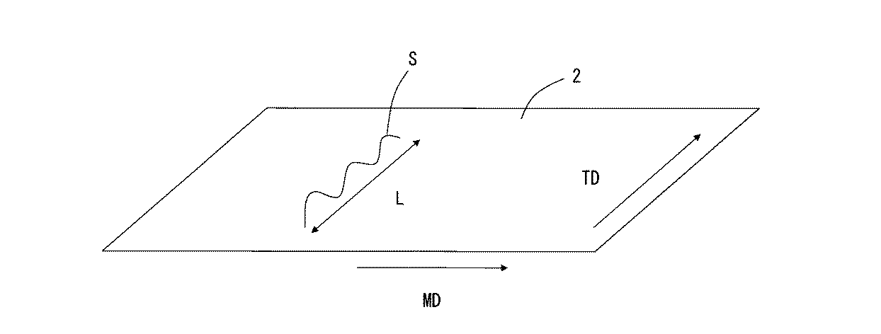
表1から明らかなように、Wsmが2.5〜20.0mmである各実施例の場合、厚みが薄くてもCCL製造時のラミネート処理における銅箔のシワの発生を抑制できた。又、CCLの屈曲性、密着性も優れていた。
特に、Wzが0.00010〜0.00200mmである実施例1〜16の場合、その他の実施例に比べ、ラミネート処理における銅箔のシワの発生をさらに有効に抑制できた。
As is apparent from Table 1, in each Example where Wsm was 2.5 to 20.0 mm, it was possible to suppress the occurrence of wrinkling of the copper foil in the laminating process during CCL manufacture even when the thickness was small. Moreover, the flexibility and adhesion of CCL were also excellent.
In particular, in Examples 1 to 16 in which Wz was 0.00010 to 0.00200 mm, it was possible to more effectively suppress the occurrence of copper foil wrinkles in the laminating process as compared with the other examples.
一方、Wsmが2.5mm未満の比較例1、3,及びWsmが20.0mmを超えた比較例2の場合、CCL製造時のラミネート処理における銅箔にシワが顕著に発生した。
又、比較例2の場合、Ra及び Rzが規定範囲未満となり、銅箔表面が平坦過ぎて密着性も低下した。
On the other hand, in the case of Comparative Examples 1 and 3 where Wsm is less than 2.5 mm and Comparative Example 2 where Wsm exceeds 20.0 mm, wrinkles were remarkably generated in the copper foil in the laminating process during CCL production.
In the case of Comparative Example 2, Ra and Rz were less than the specified range, the copper foil surface was too flat, and the adhesion was also lowered.
2 銅箔の表面
L TD方向に沿う50mmの長さ
S 断面曲線
2 Copper foil surface L Length of 50mm along TD direction S Sectional curve
Claims (8)
JIS-B0601(2013)に従い、TD方向に沿う50mmの長さの表面の断面曲線から、輪郭曲線フィルタλc=2 mm,輪郭曲線フィルタλf=25mmの条件で短波長及び長波長成分をカットオフしてうねり曲線を求めたとき、うねり曲線要素の平均長さWsmが2.5〜20.0mmであることを特徴とする銅箔。 A copper foil having a thickness of 3 to 8 μm containing 99.90% or more of copper by mass,
In accordance with JIS-B0601 (2013), the short wavelength and long wavelength components are cut off from the cross-sectional curve of the surface with a length of 50 mm along the TD direction under the conditions of contour curve filter λc = 2 mm and contour curve filter λf = 25 mm. A copper foil characterized in that the mean length Wsm of the undulation curve element is 2.5 to 20.0 mm when the undulation curve is obtained.
Priority Applications (4)
| Application Number | Priority Date | Filing Date | Title |
|---|---|---|---|
| JP2016067413A JP6612168B2 (en) | 2016-03-30 | 2016-03-30 | Copper foil, copper clad laminate, flexible printed circuit board and electronic device |
| TW106104689A TWI660838B (en) | 2016-03-30 | 2017-02-14 | Copper foil, copper-clad laminated board, flexible printed circuit board, and electronic device |
| KR1020170029383A KR102021175B1 (en) | 2016-03-30 | 2017-03-08 | Copper foil, copper-clad laminate, and flexible printed wiring board and electronic device |
| CN201710201765.5A CN107278015B (en) | 2016-03-30 | 2017-03-30 | Copper foil, copper clad laminates, and flexible printed substrates and electronic devices |
Applications Claiming Priority (1)
| Application Number | Priority Date | Filing Date | Title |
|---|---|---|---|
| JP2016067413A JP6612168B2 (en) | 2016-03-30 | 2016-03-30 | Copper foil, copper clad laminate, flexible printed circuit board and electronic device |
Publications (2)
| Publication Number | Publication Date |
|---|---|
| JP2017183459A true JP2017183459A (en) | 2017-10-05 |
| JP6612168B2 JP6612168B2 (en) | 2019-11-27 |
Family
ID=60008231
Family Applications (1)
| Application Number | Title | Priority Date | Filing Date |
|---|---|---|---|
| JP2016067413A Active JP6612168B2 (en) | 2016-03-30 | 2016-03-30 | Copper foil, copper clad laminate, flexible printed circuit board and electronic device |
Country Status (4)
| Country | Link |
|---|---|
| JP (1) | JP6612168B2 (en) |
| KR (1) | KR102021175B1 (en) |
| CN (1) | CN107278015B (en) |
| TW (1) | TWI660838B (en) |
Cited By (3)
| Publication number | Priority date | Publication date | Assignee | Title |
|---|---|---|---|---|
| JP2020158841A (en) * | 2019-03-27 | 2020-10-01 | Jx金属株式会社 | Rolled copper foil coil |
| JP2022035805A (en) * | 2020-08-21 | 2022-03-04 | Agc株式会社 | Method for manufacturing laminated plate and laminated plate |
| JP2023551759A (en) * | 2020-11-02 | 2023-12-13 | アルビス シュトルベルグ ゲーエムベーハー アンド シーオー ケイジー | copper ceramic substrate |
Families Citing this family (1)
| Publication number | Priority date | Publication date | Assignee | Title |
|---|---|---|---|---|
| JP6856688B2 (en) * | 2019-03-26 | 2021-04-07 | Jx金属株式会社 | Copper foil for flexible printed circuit boards, copper-clad laminates using it, flexible printed circuit boards, and electronic devices |
Citations (4)
| Publication number | Priority date | Publication date | Assignee | Title |
|---|---|---|---|---|
| WO2007105635A1 (en) * | 2006-03-10 | 2007-09-20 | Mitsui Mining & Smelting Co., Ltd. | Surface treated elctrolytic copper foil and process for producing the same |
| JP2009176768A (en) * | 2008-01-21 | 2009-08-06 | Ube Ind Ltd | Manufacturing method of copper wiring insulating film by semi-additive method, and copper wiring insulating film manufactured therefrom |
| WO2010090352A1 (en) * | 2009-02-09 | 2010-08-12 | 新日本製鐵株式会社 | Titanium material for hot rolling and manufacturing method thereof |
| JP2013191638A (en) * | 2012-03-12 | 2013-09-26 | Jx Nippon Mining & Metals Corp | Rolled copper foil for printed wiring board |
Family Cites Families (7)
| Publication number | Priority date | Publication date | Assignee | Title |
|---|---|---|---|---|
| JP4410021B2 (en) | 2004-04-19 | 2010-02-03 | 株式会社カネカ | Method for producing flexible metal-clad laminate with improved productivity and flexible metal-clad laminate obtained thereby |
| JP4941407B2 (en) | 2008-06-02 | 2012-05-30 | 東洋紡績株式会社 | Copper-clad laminate and method for producing copper-clad laminate |
| JP5094834B2 (en) * | 2009-12-28 | 2012-12-12 | Jx日鉱日石金属株式会社 | Copper foil manufacturing method, copper foil and copper clad laminate |
| JP2011230308A (en) | 2010-04-23 | 2011-11-17 | Panasonic Electric Works Co Ltd | Flexible copper-clad laminated sheet and flexible printed wiring board |
| CN102586831B (en) * | 2012-03-12 | 2014-11-19 | 山东金宝电子股份有限公司 | Surface treatment process for reducing roughness of electrolytic copper foil |
| JP5261595B1 (en) * | 2012-06-29 | 2013-08-14 | Jx日鉱日石金属株式会社 | Rolled copper foil, method for producing the same, and laminate |
| JP6393126B2 (en) * | 2013-10-04 | 2018-09-19 | Jx金属株式会社 | Surface-treated rolled copper foil, laminate, printed wiring board, electronic device, and printed wiring board manufacturing method |
-
2016
- 2016-03-30 JP JP2016067413A patent/JP6612168B2/en active Active
-
2017
- 2017-02-14 TW TW106104689A patent/TWI660838B/en active
- 2017-03-08 KR KR1020170029383A patent/KR102021175B1/en active Active
- 2017-03-30 CN CN201710201765.5A patent/CN107278015B/en active Active
Patent Citations (4)
| Publication number | Priority date | Publication date | Assignee | Title |
|---|---|---|---|---|
| WO2007105635A1 (en) * | 2006-03-10 | 2007-09-20 | Mitsui Mining & Smelting Co., Ltd. | Surface treated elctrolytic copper foil and process for producing the same |
| JP2009176768A (en) * | 2008-01-21 | 2009-08-06 | Ube Ind Ltd | Manufacturing method of copper wiring insulating film by semi-additive method, and copper wiring insulating film manufactured therefrom |
| WO2010090352A1 (en) * | 2009-02-09 | 2010-08-12 | 新日本製鐵株式会社 | Titanium material for hot rolling and manufacturing method thereof |
| JP2013191638A (en) * | 2012-03-12 | 2013-09-26 | Jx Nippon Mining & Metals Corp | Rolled copper foil for printed wiring board |
Cited By (6)
| Publication number | Priority date | Publication date | Assignee | Title |
|---|---|---|---|---|
| JP2020158841A (en) * | 2019-03-27 | 2020-10-01 | Jx金属株式会社 | Rolled copper foil coil |
| KR20200115281A (en) | 2019-03-27 | 2020-10-07 | 제이엑스금속주식회사 | Rolled copper foil coil |
| CN111757598A (en) * | 2019-03-27 | 2020-10-09 | 捷客斯金属株式会社 | Rolled Copper Foil Coil |
| JP2022035805A (en) * | 2020-08-21 | 2022-03-04 | Agc株式会社 | Method for manufacturing laminated plate and laminated plate |
| JP7476721B2 (en) | 2020-08-21 | 2024-05-01 | Agc株式会社 | Manufacturing method of laminate and laminate |
| JP2023551759A (en) * | 2020-11-02 | 2023-12-13 | アルビス シュトルベルグ ゲーエムベーハー アンド シーオー ケイジー | copper ceramic substrate |
Also Published As
| Publication number | Publication date |
|---|---|
| CN107278015A (en) | 2017-10-20 |
| KR102021175B1 (en) | 2019-09-11 |
| CN107278015B (en) | 2019-10-18 |
| TWI660838B (en) | 2019-06-01 |
| KR20170113092A (en) | 2017-10-12 |
| TW201733797A (en) | 2017-10-01 |
| JP6612168B2 (en) | 2019-11-27 |
Similar Documents
| Publication | Publication Date | Title |
|---|---|---|
| JP5611355B2 (en) | Metal-clad laminate | |
| EP2383113B1 (en) | Metal foil with carrier | |
| CN112839812B (en) | Metal clad laminate and method for manufacturing metal clad laminate | |
| JP6612168B2 (en) | Copper foil, copper clad laminate, flexible printed circuit board and electronic device | |
| EP2383114B1 (en) | Metal foil with carrier | |
| TW200533264A (en) | Method for producing flexible laminate | |
| JP2017179393A (en) | Rolled copper foil, copper clad laminate, flexible printed circuit board, and electronic device | |
| JP6170516B2 (en) | Rolled copper foil and manufacturing method thereof, copper-clad laminate, flexible printed circuit board, and electronic device | |
| JP5217321B2 (en) | Method for producing flexible metal laminate | |
| JP2023127191A (en) | Metal-clad laminate and method for manufacturing the same | |
| JP2016176094A (en) | Rolled copper foil, copper-clad laminate, and flexible printed board and electronic equipment | |
| JP4389627B2 (en) | Method for producing flexible metal laminate | |
| JP2002052614A (en) | Manufacturing method of laminated board | |
| JP2009071021A (en) | Method for manufacturing multilayer printed circuit board | |
| JP2007109694A (en) | Method for producing single-sided flexible metal laminate | |
| JP4706283B2 (en) | Method for producing heat-resistant flexible metal laminate | |
| JP6827022B2 (en) | Copper foil for flexible printed circuit boards, copper-clad laminates using it, flexible printed circuit boards, and electronic devices | |
| JP2008074037A (en) | Method for producing heat-resistant flexible metal laminate | |
| JP7675510B2 (en) | Manufacturing method of metal-clad laminate | |
| JP3954831B2 (en) | Method for producing heat-resistant flexible laminate | |
| JP6081883B2 (en) | Copper foil, laminated board using the same, method for manufacturing electronic device, and method for manufacturing printed wiring board | |
| TW202448701A (en) | Flexible metal-clad laminate and manufacturing method thereof | |
| JP2025147696A (en) | Flexible metal-clad laminate and method for manufacturing same | |
| JP2009269267A (en) | Method of manufacturing metal laminated sheet | |
| JP2007223053A (en) | Method for producing heat-resistant flexible metal laminate |
Legal Events
| Date | Code | Title | Description |
|---|---|---|---|
| A621 | Written request for application examination |
Free format text: JAPANESE INTERMEDIATE CODE: A621 Effective date: 20180928 |
|
| A977 | Report on retrieval |
Free format text: JAPANESE INTERMEDIATE CODE: A971007 Effective date: 20190531 |
|
| A131 | Notification of reasons for refusal |
Free format text: JAPANESE INTERMEDIATE CODE: A131 Effective date: 20190702 |
|
| A521 | Request for written amendment filed |
Free format text: JAPANESE INTERMEDIATE CODE: A523 Effective date: 20190805 |
|
| TRDD | Decision of grant or rejection written | ||
| A01 | Written decision to grant a patent or to grant a registration (utility model) |
Free format text: JAPANESE INTERMEDIATE CODE: A01 Effective date: 20191021 |
|
| A61 | First payment of annual fees (during grant procedure) |
Free format text: JAPANESE INTERMEDIATE CODE: A61 Effective date: 20191030 |
|
| R150 | Certificate of patent or registration of utility model |
Ref document number: 6612168 Country of ref document: JP Free format text: JAPANESE INTERMEDIATE CODE: R150 |
|
| S531 | Written request for registration of change of domicile |
Free format text: JAPANESE INTERMEDIATE CODE: R313531 |
|
| R350 | Written notification of registration of transfer |
Free format text: JAPANESE INTERMEDIATE CODE: R350 |
|
| R250 | Receipt of annual fees |
Free format text: JAPANESE INTERMEDIATE CODE: R250 |
|
| R250 | Receipt of annual fees |
Free format text: JAPANESE INTERMEDIATE CODE: R250 |
|
| R250 | Receipt of annual fees |
Free format text: JAPANESE INTERMEDIATE CODE: R250 |