JP2017190425A - Granular resin composition for semiconductor sealing and semiconductor device - Google Patents
Granular resin composition for semiconductor sealing and semiconductor device Download PDFInfo
- Publication number
- JP2017190425A JP2017190425A JP2016081866A JP2016081866A JP2017190425A JP 2017190425 A JP2017190425 A JP 2017190425A JP 2016081866 A JP2016081866 A JP 2016081866A JP 2016081866 A JP2016081866 A JP 2016081866A JP 2017190425 A JP2017190425 A JP 2017190425A
- Authority
- JP
- Japan
- Prior art keywords
- resin composition
- mass
- spherical alumina
- semiconductor
- granular
- Prior art date
- Legal status (The legal status is an assumption and is not a legal conclusion. Google has not performed a legal analysis and makes no representation as to the accuracy of the status listed.)
- Granted
Links
Landscapes
- Compositions Of Macromolecular Compounds (AREA)
- Epoxy Resins (AREA)
- Structures Or Materials For Encapsulating Or Coating Semiconductor Devices Or Solid State Devices (AREA)
Abstract
【課題】熱伝導性、融け性、流動性に優れ、封止時のワイヤの変形および樹脂漏れを低減/防止できる粉粒状半導体封止用樹脂組成物、及びそれを用いた半導体装置を提供する。【解決手段】(A)エポキシ樹脂、(B)フェノール樹脂硬化剤、(C)硬化促進剤、及び(D)球状アルミナを含有する粉粒状半導体封止用樹脂組成物であって、前記(D)球状アルミナは、該樹脂組成物中に80質量%以上95質量%未満含まれるとともに、(D1)粒径2μm未満の球状アルミナを5〜25質量%含有する粉粒状半導体封止用樹脂組成物、および該組成物により半導体素子が封止された半導体装置。【選択図】なしPROBLEM TO BE SOLVED: To provide a resin composition for powdery and granular semiconductor encapsulation, which has excellent thermal conductivity, meltability and fluidity, and can reduce/prevent wire deformation and resin leakage during encapsulation, and a semiconductor device using the same. .. A powder-granular semiconductor encapsulating resin composition containing (A) an epoxy resin, (B) a phenol resin curing agent, (C) a curing accelerator, and (D) spherical alumina. ) Spherical alumina is contained in the resin composition in an amount of 80% by mass or more and less than 95% by mass, and (D1) 5 to 25% by mass of spherical alumina having a particle size of less than 2 μm. And a semiconductor device in which a semiconductor element is sealed with the composition. [Selection diagram] None
Description
本発明は、粉粒状半導体封止用樹脂組成物、及びこれを用いた半導体装置に関する。 The present invention relates to a granular semiconductor sealing resin composition and a semiconductor device using the same.
近年、電子部品のプリント配線板への高密度実装化に伴い、IC、LSI等の半導体装置は従来の挿入型パッケージから表面実装型パッケージにその主流が変わってきている。表面実装型では、半導体素子のパッケージに対する占有体積も大きくなり、パッケージの肉厚は非常に薄くなっている。また、素子の多機能化、大容量化によって、チップ面積の増大、多ピン化が進み、さらにパッド数の増加によって、パッドピッチおよびパッドサイズの縮小化、いわゆる狭パッドピッチ化も進んでいる。また、それに伴い発熱量も増大している。 In recent years, with the high density mounting of electronic components on printed wiring boards, the mainstream of semiconductor devices such as ICs and LSIs has changed from conventional insertion type packages to surface mounting type packages. In the surface mounting type, the occupied volume of the semiconductor element with respect to the package is increased, and the thickness of the package is very thin. In addition, the increase in the number of pads and the increase in the number of pads have progressed with the increase in the number of pads and the increase in the number of pads. Along with this, the amount of heat generation also increases.
一方、半導体素子を搭載する基板は、半導体素子ほどの電極間隔の狭ピッチ化は困難である。このため、半導体素子から引き出すワイヤ長を長くするか、またはワイヤを細線化することにより上記多ピン化、狭パッドピッチ化に対応している。しかし、ワイヤが細くなると、従来のトランスファー成形による封止方法では、ワイヤが樹脂の注入圧力により流され易くなる。特に、サイドゲート方式では、ワイヤに加わる樹脂の注入圧力が大きいため、この傾向が著しい。 On the other hand, it is difficult for a substrate on which a semiconductor element is mounted to reduce the electrode pitch as much as the semiconductor element. For this reason, the wire length drawn out from the semiconductor element is lengthened or the wire is thinned to cope with the above-mentioned multi-pin and narrow pad pitch. However, when the wire is thinned, the wire is easily flown by the injection pressure of the resin in the sealing method by the conventional transfer molding. In particular, in the side gate method, this tendency is remarkable because the injection pressure of the resin applied to the wire is large.
そのため、半導体素子等の電子素子の樹脂封止方法として、いわゆる圧縮成形法が用いられるようになってきている(例えば、特許文献1、2参照)。この圧縮成形法においては、金型内に被封止物(例えば、半導体素子等の電子素子が設けられた基板等)を保持し、これに対向させるように粉粒状樹脂組成物を供給し、被封止物と粉粒状樹脂組成物とを圧縮することで樹脂封止が行われる。 Therefore, a so-called compression molding method has been used as a resin sealing method for electronic elements such as semiconductor elements (for example, see Patent Documents 1 and 2). In this compression molding method, an object to be sealed (for example, a substrate on which an electronic element such as a semiconductor element is provided) is held in a mold, and a granular resin composition is supplied so as to face this, Resin sealing is performed by compressing the object to be sealed and the granular resin composition.
圧縮成形法によれば、溶融した粉粒状樹脂組成物が被封止物の主面に略平行な方向に流動するため、流動量を少なくすることができ、樹脂の流れによる被封止物の破損、特に、ワイヤボンディングされた配線の破損を低減させることができる。 According to the compression molding method, since the molten granular resin composition flows in a direction substantially parallel to the main surface of the object to be sealed, the amount of flow can be reduced, and the object to be sealed by the flow of the resin can be reduced. Breakage, in particular, breakage of the wire-bonded wiring can be reduced.
しかし、半導体パッケージの肉厚がより薄くなり、半導体素子を接続するワイヤがより長く、またより細線化されると、ワイヤの変形発生のおそれが高くなる。このため、融け性及び流動性がより良好な粉粒状半導体封止用樹脂組成物が求められている。 However, if the thickness of the semiconductor package is reduced, the wires connecting the semiconductor elements are longer and the wires are further thinned, the risk of deformation of the wires increases. For this reason, the resin composition for a granular semiconductor sealing with more favorable meltability and fluidity | liquidity is calculated | required.
また、粉粒状半導体封止用樹脂組成物の融け性や流動性が向上すると、ワイヤの変形発生は抑制されるが、半導体装置成形時の減圧下において、加熱溶融した樹脂が飛散する、いわゆる「樹脂漏れ」という現象が発生しやすくなる。特に、球状アルミナを含む高熱伝導性の粉粒状半導体封止用樹脂組成物において、この傾向が顕著であった。 In addition, when the meltability and fluidity of the resin composition for encapsulating a granular semiconductor are improved, the occurrence of wire deformation is suppressed, but the heat-melted resin scatters under reduced pressure during molding of the semiconductor device. The phenomenon of “resin leakage” tends to occur. This tendency was particularly remarkable in the resin composition for encapsulating granular semiconductors containing spherical alumina.
本発明は上記従来技術の課題に対処してなされたもので、熱伝導性、融け性、流動性に優れ、封止時のワイヤの変形を低減できるとともに、樹脂漏れも防止できる新規な粉粒状半導体封止用樹脂組成物、及びそのような粉粒状半導体封止用樹脂組成物を用いて封止された、高熱伝導性で、かつワイヤの変化や樹脂漏れのない、高い信頼性を備えた半導体装置を提供することを目的としている。 The present invention has been made in response to the above-mentioned problems of the prior art, and is excellent in thermal conductivity, meltability, fluidity, can reduce deformation of the wire during sealing, and can prevent resin leakage. Resin composition for semiconductor encapsulation, and sealed with such a granular semiconductor encapsulation resin composition, with high thermal conductivity and high reliability without wire change and resin leakage An object is to provide a semiconductor device.
本発明者らは、上記の課題を解決するために鋭意研究を重ねた結果、特定の粒度分布を有する球状アルミナを特定量含有させることによって、高熱伝導性を維持しつつ、ワイヤの変形を低減し、かつ樹脂漏れも抑制できることを見出し、本発明を完成するに至った。
すなわち、本発明は、以下の[1]〜[6]の構成を有する、粉粒状半導体封止用樹脂組成物及び半導体装置である。
[1](A)エポキシ樹脂、(B)フェノール樹脂硬化剤、(C)硬化促進剤、及び(D)球状アルミナを含有する粉粒状半導体封止用樹脂組成物であって、
前記(D)球状アルミナは、該樹脂組成物中に80質量%以上95質量%未満含まれるとともに、(D1)粒径2μm未満の球状アルミナを5〜25質量%含有することを特徴とする粉粒状半導体封止用樹脂組成物。
[2]前記(D)球状アルミナは、(D2)粒径2μm以上20μm未満の球状アルミナを45〜65質量%、(D3)粒径20μm以上の球状アルミナを15〜35質量%含有することを特徴とする[1]の粉粒状半導体封止用樹脂組成物。
[3]前記(D)球状アルミナは、(D31)粒径20μm以上60μm未満の球状アルミナを10〜30質量%、(D32)粒径60μm以上の球状アルミナを5〜25質量%含有することを特徴とする[2]の粉粒状半導体封止用樹脂組成物。
[4]さらに、(E)可塑剤として、融点が100〜170℃の有機リン化合物を0.1〜1質量%含有することを特徴とする[1]乃至[3]のいずれかの粉粒状半導体封止用樹脂組成物。
[5]該粉粒状半導体封止用樹脂組成物を、加熱溶融させた後の溶融表面のデジタル画像から得られる輝度値のヒストグラムにおいて、中央値が50以下であることを特徴とする[1]乃至[4]のいずれかの粉粒状半導体封止用樹脂組成物。
[6][1]乃至[5]のいずれかの粉粒状半導体封止用樹脂組成物により、半導体素子が封止されていることを特徴とする半導体装置。
As a result of intensive research to solve the above problems, the present inventors have reduced the deformation of the wire while maintaining high thermal conductivity by containing a specific amount of spherical alumina having a specific particle size distribution. In addition, the present inventors have found that resin leakage can be suppressed and have completed the present invention.
That is, this invention is the resin composition for granular semiconductor sealing and semiconductor device which have the structure of the following [1]-[6].
[1] A resin composition for encapsulating a granular semiconductor comprising (A) an epoxy resin, (B) a phenol resin curing agent, (C) a curing accelerator, and (D) spherical alumina,
The (D) spherical alumina is contained in the resin composition in an amount of 80% by mass or more and less than 95% by mass, and (D1) a powder containing 5 to 25% by mass of spherical alumina having a particle size of less than 2 μm. Granular semiconductor encapsulating resin composition.
[2] The (D) spherical alumina contains (D2) 45 to 65% by mass of spherical alumina having a particle size of 2 μm or more and less than 20 μm, and (D3) 15 to 35% by mass of spherical alumina having a particle size of 20 μm or more. [1] A resin composition for encapsulating a granular semiconductor according to [1].
[3] The (D) spherical alumina contains (D31) 10-30% by mass of spherical alumina having a particle size of 20 μm or more and less than 60 μm, and (D32) 5-25% by mass of spherical alumina having a particle size of 60 μm or more. [2] A resin composition for encapsulating a granular semiconductor, which is characterized.
[4] Furthermore, 0.1 to 1% by mass of an organophosphorus compound having a melting point of 100 to 170 ° C. is contained as (E) a plasticizer, and any one of [1] to [3] Semiconductor sealing resin composition.
[5] In a histogram of luminance values obtained from a digital image of the melted surface after the resin composition for encapsulating a granular semiconductor is heated and melted, the median is 50 or less [1] The resin composition for granular semiconductor sealing in any one of thru | or [4].
[6] A semiconductor device, wherein a semiconductor element is sealed with the granular semiconductor sealing resin composition of any one of [1] to [5].
本発明の粉粒状半導体封止用樹脂組成物によれば、樹脂組成物の熱伝導性、融け性および流動性を所望の特性とし、ワイヤの変形が抑制され、かつ樹脂漏れも少ない、成形性に優れた封止を行うことができる。 According to the resin composition for encapsulating a granular semiconductor of the present invention, the thermal conductivity, meltability and fluidity of the resin composition are desired characteristics, the deformation of the wire is suppressed, and the resin leakage is small, and the moldability Excellent sealing can be performed.
また、本発明の半導体装置によれば、上記粉粒状半導体封止用樹脂組成物を用いて封止しているため、高熱伝導性で、ワイヤの変化や樹脂漏れのない、高い信頼性を備えた半導体装置を得ることができる。 In addition, according to the semiconductor device of the present invention, since it is sealed using the above resin composition for encapsulating a granular semiconductor, it has high thermal conductivity, high reliability without wire change and resin leakage. A semiconductor device can be obtained.
以下、本発明を詳細に説明する。
本発明の粉粒状半導体封止用樹脂組成物は、(A)エポキシ樹脂、(B)フェノール樹脂硬化剤、(C)硬化促進剤、及び(D)球状アルミナを含有するものである。
Hereinafter, the present invention will be described in detail.
The resin composition for encapsulating a granular semiconductor of the present invention contains (A) an epoxy resin, (B) a phenol resin curing agent, (C) a curing accelerator, and (D) spherical alumina.
本発明で使用する(A)成分のエポキシ樹脂は、1分子中に2個以上のエポキシ基を有するものであれば、分子構造、分子量等に制限されることなく一般に電子部品の封止材料として使用されているものを広く用いることができるが、なかでも、ビフェニル骨格を有するエポキシ樹脂、すなわちビフェニル型エポキシ樹脂が好ましい。なお、本発明におけるビフェニル骨格には、ビフェニル環のうち少なくとも一方の芳香族環が水素添加されているものも含まれる。 The epoxy resin of component (A) used in the present invention is generally not limited by the molecular structure, molecular weight, etc. as long as it has two or more epoxy groups in one molecule, and is generally used as a sealing material for electronic components. Although what is used can be widely used, the epoxy resin which has biphenyl frame | skeleton, ie, a biphenyl type epoxy resin, is preferable especially. The biphenyl skeleton in the present invention includes those in which at least one aromatic ring is hydrogenated among the biphenyl rings.
ビフェニル型エポキシ樹脂の具体例としては、例えば、4,4´−ビス(2,3−エポキシプロポキシ)ビフェニル、4,4´−ビス(2,3−エポキシプロポキシ)−3,3´,5,5´−テトラメチルビフェニル、エピクロルヒドリンと4,4´−ビフェノールまたは4,4´−(3,3´,5,5´−テトラメチル)ビフェノール等のビフェノール化合物とを反応させて得られるエポキシ樹脂等が挙げられる。なかでも、4,4´−ビス(2,3−エポキシプロポキシ)−3,3´,5,5´−テトラメチルビフェニル、4,4´−ジヒドロキシ−3,3´,5,5´−テトラメチルビフェニルのグリシジルエーテルが好ましい。
市販品を例示すると、例えば、三菱化学(株)製のYX−4000(エポキシ当量185)、同YX−4000H(エポキシ当量193)、日本化薬(株)製のNC−3000(エポキシ当量273)、同NC−3000H(エポキシ当量288)(以上、いずれも商品名)等が挙げられる。
ビフェニル型エポキシ樹脂の使用によって、(D)成分の球状アルミナを多量に配合しても溶融粘度を最適範囲に維持することができ、また耐熱性に優れる半導体封止用樹脂組成物を得ることができる。なお、エポキシ樹脂は、1種を単独で使用してもよく、2種以上を組み合わせて使用してもよい。
Specific examples of the biphenyl type epoxy resin include, for example, 4,4′-bis (2,3-epoxypropoxy) biphenyl, 4,4′-bis (2,3-epoxypropoxy) -3,3 ′, 5, Epoxy resins obtained by reacting 5′-tetramethylbiphenyl, epichlorohydrin and biphenol compounds such as 4,4′-biphenol or 4,4 ′-(3,3 ′, 5,5′-tetramethyl) biphenol, etc. Is mentioned. Among them, 4,4′-bis (2,3-epoxypropoxy) -3,3 ′, 5,5′-tetramethylbiphenyl, 4,4′-dihydroxy-3,3 ′, 5,5′-tetra Methyl biphenyl glycidyl ether is preferred.
Examples of commercially available products include YX-4000 (epoxy equivalent 185) and YX-4000H (epoxy equivalent 193) manufactured by Mitsubishi Chemical Corporation, NC-3000 (epoxy equivalent 273) manufactured by Nippon Kayaku Co., Ltd. NC-3000H (epoxy equivalent 288) (all are trade names).
By using a biphenyl type epoxy resin, the melt viscosity can be maintained in the optimum range even when a large amount of the spherical alumina of the component (D) is blended, and a semiconductor sealing resin composition having excellent heat resistance can be obtained. it can. In addition, an epoxy resin may be used individually by 1 type, and may be used in combination of 2 or more type.
本発明で使用する(B)成分のフェノール樹脂硬化剤は、1分子当たり2個以上のフェノール性水酸基を有し、上記(A)成分のエポキシ樹脂を硬化させることができるものであって、電子部品の封止材料として一般に用いられるものであれば特に制限されることなく使用できる。 The (B) component phenolic resin curing agent used in the present invention has two or more phenolic hydroxyl groups per molecule and can cure the above (A) component epoxy resin. Any material that is generally used as a sealing material for components can be used without any particular limitation.
フェノール樹脂硬化剤の具体例としては、例えば、フェノールノボラック樹脂、クレゾールノボラック樹脂、アラルキル型フェノール樹脂、ナフタレン型フェノール樹脂、シクロペンタジエン型フェノール樹脂、トリフェノールアルカン型フェノール樹脂等が挙げられる。これらは1種を単独で使用してもよく、2種以上を組み合わせて使用してもよい。 Specific examples of the phenol resin curing agent include phenol novolac resin, cresol novolac resin, aralkyl type phenol resin, naphthalene type phenol resin, cyclopentadiene type phenol resin, triphenol alkane type phenol resin and the like. These may be used individually by 1 type and may be used in combination of 2 or more type.
本発明の組成物における(A)成分のエポキシ樹脂と(B)成分のフェノール樹脂硬化剤の配合比は、(A)成分のエポキシ樹脂中のエポキシ基1個に対して、(B)成分のフェノール樹脂硬化剤中のフェノール性水酸基が、好ましくは0.5〜1.6個、より好ましくは0.6〜1.4個となるように選定される。(A)エポキシ樹脂中のエポキシ基1個に対して(B)フェノール樹脂硬化剤中のフェノール性水酸基が0.5個以上であれば硬化物のガラス転移温度が良好となり、一方1.6個以下であれば、反応性が良好となるとともに、十分な架橋密度を有し、強度の高い硬化物を得ることができる。 In the composition of the present invention, the blending ratio of the epoxy resin of component (A) and the phenol resin curing agent of component (B) is that of component (B) relative to one epoxy group in the epoxy resin of component (A). The number of phenolic hydroxyl groups in the phenol resin curing agent is preferably 0.5 to 1.6, more preferably 0.6 to 1.4. (A) If the number of phenolic hydroxyl groups in the (B) phenolic resin curing agent is 0.5 or more with respect to one epoxy group in the epoxy resin, the glass transition temperature of the cured product will be good, whereas 1.6 If it is below, the reactivity will be good, and a cured product having a sufficient crosslinking density and high strength can be obtained.
本発明で使用される(C)成分の硬化促進剤は、(A)成分のエポキシ樹脂と(B)成分のフェノール樹脂硬化剤の反応を促進するものであり、かかる作用を有するものであれば特に制限されることなく使用できる。 The curing accelerator of component (C) used in the present invention is to accelerate the reaction between the epoxy resin of component (A) and the phenol resin curing agent of component (B). It can be used without any particular restrictions.
硬化促進剤の具体例としては、例えば、2−ヘプタデシルイミダゾール、2−メチルイミダゾール、2−エチルイミダゾール、2−フェニルイミダゾール、2−フェニル−4−メチルイミダゾール、4−メチルイミダゾール、4−エチルイミダゾール、2−フェニル−4−ヒドロキシメチルイミダゾール、2−エチル−4−メチルイミダゾール、1−シアノエチル−2−メチルイミダゾール、2−フェニル−4−メチル−5−ヒドロキシメチルイミダゾール、2−フェニル−4,5−ジヒドロキシメチルイミダゾール、2−ウンデシルイミダゾール、1−ベンジル−2−メチルイミダゾール、1−ベンジル−2−フェニルイミダゾール、1−シアノエチル−2−メチルイミダゾール、1−シアノエチル−2−エチル−4−メチルイミダゾール、1−シアノエチル−2−ウンデシルイミダゾール、1−シアノエチル−2−フェニルイミダゾール、1−シアノエチル−2−ウンデシルイミダゾリウムトリメリテイト、2,4−ジアミノ−6−[2′−メチルイミダゾリル−(1′)]−エチル−s−トリアジン、2,4−ジアミノ−6−[2′−ウンデシルイミダゾリル−(1′)]−エチル−s−トリアジン、2,4−ジアミノ−6−[2′−エチル−4′−メチルイミダゾリル−(1′)]−エチル−s−トリアジン、2,4−ジアミノ−6−[2′−メチルイミダゾリル−(1′)]−エチル−s−トリアジン、2−フェニルイミダゾールイソシアヌル酸付加物、2−メチルイミダゾールイソシアヌル酸付加物、2−フェニルイミダゾリン等のイミダゾール類;1,8−ジアザビシクロ[5,4,0]ウンデセン−7(DBU)、1,5−ジアザビシクロ[4,3,0]ノネン、5,6−ジブチルアミノ−1,8−ジアザビシクロ[5,4,0]ウンデセン−7等のジアザビシクロ化合物およびこれらの塩;トリエチルアミン、トリエチレンジアミン、ベンジルジメチルアミン、α−メチルベンジルジメチルアミン、トリエタノールアミン、ジメチルアミノエタノール、トリス(ジメチルアミノメチル)フェノール等の三級アミン類;トリメチルホスフィン、トリエチルホスフィン、トリブチルホスフィン、ジフェニルホスフィン、トリフェニルホスフィン、トリ(p‐メチルフェニル)ホスフィン、トリ(ノニルフェニル)ホスフィン、メチルジフェニルホスフィン、ジブチルフェニルホスフィン、トリシクロヘキシルホスフィン、ビス(ジフェニルホスフィノ)メタン、1,2‐ビス(ジフェニルホスフィノ)エタン等の有機ホスフィン化合物;テトラフェニルホスホニウムテトラフェニルボレート、トリフェニルホスフィンテトラフェニルボレート、トリフェニルホスフィントリフェニルボラン等のテトラ‐またはトリフェニルボロン塩等が挙げられる。これらは1種を単独で使用してもよく、2種以上を組み合わせて使用してもよい。(C)硬化促進剤としては、なかでも、流動性、成形性が良好である等の観点から、イミダゾール類が好ましい。 Specific examples of the curing accelerator include, for example, 2-heptadecylimidazole, 2-methylimidazole, 2-ethylimidazole, 2-phenylimidazole, 2-phenyl-4-methylimidazole, 4-methylimidazole, 4-ethylimidazole. 2-phenyl-4-hydroxymethylimidazole, 2-ethyl-4-methylimidazole, 1-cyanoethyl-2-methylimidazole, 2-phenyl-4-methyl-5-hydroxymethylimidazole, 2-phenyl-4,5 -Dihydroxymethylimidazole, 2-undecylimidazole, 1-benzyl-2-methylimidazole, 1-benzyl-2-phenylimidazole, 1-cyanoethyl-2-methylimidazole, 1-cyanoethyl-2-ethyl-4-methylimidazole 1-cyanoethyl-2-undecylimidazole, 1-cyanoethyl-2-phenylimidazole, 1-cyanoethyl-2-undecylimidazolium trimellitate, 2,4-diamino-6- [2'-methylimidazolyl- (1 ')]-Ethyl-s-triazine, 2,4-diamino-6- [2'-undecylimidazolyl- (1')]-ethyl-s-triazine, 2,4-diamino-6- [2'- Ethyl-4'-methylimidazolyl- (1 ')]-ethyl-s-triazine, 2,4-diamino-6- [2'-methylimidazolyl- (1')]-ethyl-s-triazine, 2-phenyl Imidazole isocyanuric acid adducts, 2-methylimidazole isocyanuric acid adducts, imidazoles such as 2-phenylimidazoline; 1,8-diazabi Chlo [5,4,0] undecene-7 (DBU), 1,5-diazabicyclo [4,3,0] nonene, 5,6-dibutylamino-1,8-diazabicyclo [5,4,0] undecene Diazabicyclo compounds such as 7 and salts thereof; tertiary amines such as triethylamine, triethylenediamine, benzyldimethylamine, α-methylbenzyldimethylamine, triethanolamine, dimethylaminoethanol, tris (dimethylaminomethyl) phenol; trimethylphosphine , Triethylphosphine, tributylphosphine, diphenylphosphine, triphenylphosphine, tri (p-methylphenyl) phosphine, tri (nonylphenyl) phosphine, methyldiphenylphosphine, dibutylphenylphosphine, tricyclohexyl Organic phosphine compounds such as sphin, bis (diphenylphosphino) methane, 1,2-bis (diphenylphosphino) ethane; tetraphenylphosphonium tetraphenylborate, triphenylphosphine tetraphenylborate, tetraphenylphosphine triphenylborane, etc. -Or triphenylboron salt and the like. These may be used individually by 1 type and may be used in combination of 2 or more type. As the (C) curing accelerator, imidazoles are preferable from the viewpoint of good fluidity and moldability.
この硬化促進剤の配合量は、(A)成分のエポキシ樹脂と(B)成分のフェノール樹脂硬化剤の合計量100質量部に対して、通常3〜10質量部、好ましくは4〜9質量部、より好ましくは5〜8質量部の範囲で選定される。配合量が(A)成分と(B)成分の合計量100質量部に対して、3質量部未満では、硬化性の向上にあまり効果がなく、また10質量部を超えると、組成物の流動性、成形性等が低下するおそれがある。 The blending amount of the curing accelerator is usually 3 to 10 parts by mass, preferably 4 to 9 parts by mass with respect to 100 parts by mass of the total amount of the epoxy resin (A) and the phenol resin curing agent (B). More preferably, it is selected in the range of 5 to 8 parts by mass. When the blending amount is less than 3 parts by mass with respect to 100 parts by mass of the total amount of the component (A) and the component (B), the effect of improving the curability is not so great. There is a risk that the properties, moldability, and the like are lowered.
本発明で使用する(D)成分の球状アルミナは、(D1)粒径2μm未満の球状アルミナを球状アルミナ全体の5〜25質量%含有するものである。このような微小粒径の球状アルミナを含むことで組成物に良好な融け性を付与することができる。
組成物の融け性と熱伝導性を良好にバランスさせる観点からは、(D)成分の球状アルミナは、(D1)粒径2μm未満の球状アルミナ5〜25質量%、(D2)粒径2μm以上20μm未満の球状アルミナ45〜65質量%、および(D3)粒径20μm以上の球状アルミナ15〜35質量%からなることが好ましい。
The spherical alumina of the component (D) used in the present invention contains (D1) 5 to 25% by mass of spherical alumina having a particle diameter of less than 2 μm with respect to the entire spherical alumina. By including such fine particle size spherical alumina, good meltability can be imparted to the composition.
From the viewpoint of satisfactorily balancing the meltability and thermal conductivity of the composition, the spherical alumina as component (D) is (D1) 5 to 25% by mass of spherical alumina having a particle size of less than 2 μm, and (D2) particle size of 2 μm or more. It is preferably composed of 45 to 65% by mass of spherical alumina having a particle diameter of less than 20 μm and (D3) 15 to 35% by mass of spherical alumina having a particle diameter of 20 μm or more.
さらに、(D)成分の球状アルミナが、(D1)粒径2μm未満の球状アルミナ5〜25質量%、(D2)粒径2μm以上20μm未満の球状アルミナ45〜65質量%、(D31)粒径20μm以上60μm未満の球状アルミナ10〜30質量%、(D32)粒径60μm以上の球状アルミナ5〜25質量%からなると、成形性と熱伝導性を良好にバランスさせることができ、より好ましい。通常、(D32)のような粒径60μm以上という粒径の大きい粒子が含まれると、熱伝導性が良好になる反面、成形性が低下し、ワイヤ流れも大きくなるが、上記粒度分布とすることで高密度充填が可能になり、成形性と熱伝導性を両立させることができ、また、ワイヤ流れも、特に圧縮成形法を適用した場合に、大きな粒子による影響を低減することができる。 Furthermore, the spherical alumina of the component (D) is (D1) 5 to 25% by mass of spherical alumina having a particle size of less than 2 μm, (D2) 45 to 65% by mass of spherical alumina having a particle size of 2 to 20 μm, and (D31) particle size. It is more preferable that it is composed of 10 to 30% by mass of spherical alumina having a particle size of 20 μm or more and less than 60 μm, and 5 to 25% by mass of (D32) spherical alumina having a particle size of 60 μm or more because the moldability and thermal conductivity can be well balanced. Usually, when particles having a large particle size of 60 μm or more, such as (D32), are included, the thermal conductivity is improved, but the moldability is reduced and the wire flow is increased, but the above particle size distribution is obtained. Thus, high-density filling is possible, and both formability and thermal conductivity can be achieved, and the influence of large particles can also be reduced in the wire flow particularly when the compression molding method is applied.
この(D)成分の球状アルミナの配合比は、組成物全体の80質量%以上95質量%未満であり、この範囲を外れると上記効果が得られないうえ、成型品の寸法精度、耐湿性、機械的強度等が低下する。すなわち、球状アルミナの配合比が組成物全体の80質量%未満では十分な熱伝導性が得られず、また、線膨張係数が増大して成形品の寸法精度、耐湿性、機械的強度等が低下するおそれがある。逆に、95質量%以上では、溶融粘度が増大して流動性や成形性が低下する。球状アルミナの配合比は、85〜93質量%が好ましい。 The blending ratio of the spherical alumina as the component (D) is 80% by mass or more and less than 95% by mass of the entire composition, and if it is out of this range, the above effects cannot be obtained, and the dimensional accuracy, moisture resistance, Mechanical strength and the like are reduced. That is, if the blending ratio of the spherical alumina is less than 80% by mass of the entire composition, sufficient thermal conductivity cannot be obtained, and the linear expansion coefficient is increased so that the dimensional accuracy, moisture resistance, mechanical strength, etc. of the molded product are increased. May decrease. On the contrary, if it is 95 mass% or more, melt viscosity will increase and fluidity | liquidity and a moldability will fall. The blending ratio of the spherical alumina is preferably 85 to 93% by mass.
なお、この(D)成分の球状アルミナの粒度分布は、レーザ回折・散乱法により求めることができ、例えば、(株)堀場製作所製のレーザ回折/散乱式粒度分布測定装置LA−920(製品名)により取得できる。 The particle size distribution of the spherical alumina as the component (D) can be obtained by a laser diffraction / scattering method. For example, LA-920 (product name of laser diffraction / scattering particle size distribution measuring device manufactured by Horiba, Ltd.) ).
本発明の粉粒状半導体封止用樹脂組成物には、組成物の融け性を高め、ワイヤ流れの発生を抑制するため、さらに(E)可塑剤を含有させることができる。可塑剤としては、特に、融点が100〜170℃の有機リン化合物が、分散性が良好で、添加による効果が大きいことから好ましく、なかでも、非環状ポリホスファゼン化合物、環状ホスファゼン化合物が好ましい。(E)可塑剤として、好ましい市販品を例示すると、例えば、大塚化学(株)製のSPS−100、SPB−100、SPB−100L、SPE−100、(株)伏見製薬所製のFP−100(以上、いずれも商品名)等が挙げられる。 The resin composition for encapsulating a granular semiconductor of the present invention may further contain (E) a plasticizer in order to enhance the meltability of the composition and suppress the occurrence of wire flow. As the plasticizer, an organophosphorus compound having a melting point of 100 to 170 ° C. is particularly preferable because of good dispersibility and a large effect by addition, and among them, an acyclic polyphosphazene compound and a cyclic phosphazene compound are preferable. (E) As a plasticizer, when a preferable commercial item is illustrated, for example, SPS-100, SPB-100, SPB-100L, SPE-100 manufactured by Otsuka Chemical Co., Ltd., FP-100 manufactured by Fushimi Pharmaceutical Co., Ltd. (All of the above are trade names).
この(E)成分の可塑剤の配合比は、組成物全体の0.1〜1質量%の範囲が好ましい。可塑剤の配合比が組成物全体の0.1質量%未満では添加による効果、特に融け性に対する改善効果が小さく、逆に、1質量%を超えると、硬化性が低下するおそれがある。 The blending ratio of the plasticizer as the component (E) is preferably in the range of 0.1 to 1% by mass of the entire composition. If the blending ratio of the plasticizer is less than 0.1% by mass of the entire composition, the effect of addition, particularly the effect of improving the meltability, is small, whereas if it exceeds 1% by mass, the curability may be lowered.
また、本発明の粉粒状半導体封止用樹脂組成物には、以上の各成分の他、本発明の効果を阻害しない範囲で、この種の組成物に一般に配合される、カップリング剤、充填剤(球状シリカ等)、離型剤(合成ワックス、天然ワックス、高級脂肪酸、高級脂肪酸の金属塩等)、着色剤(カーボンブラック、コバルトブルー等)、改質剤(シリコーンオイル、シリコーンゴム等)、ハイドロタルサイト類、イオン捕捉剤等の添加剤を必要に応じて配合することができる。これらの各添加剤はいずれも1種を単独で使用してもよく、2種以上を混合して使用してもよい。 In addition to the above components, the resin composition for encapsulating a granular semiconductor of the present invention is generally blended with this type of composition as long as the effects of the present invention are not impaired. Agents (spherical silica, etc.), mold release agents (synthetic wax, natural wax, higher fatty acids, higher fatty acid metal salts, etc.), colorants (carbon black, cobalt blue, etc.), modifiers (silicone oil, silicone rubber, etc.) Additives such as hydrotalcites and ion scavengers can be blended as necessary. Each of these additives may be used alone or in combination of two or more.
カップリング剤としては、エポキシシラン系、アミノシラン系、ウレイドシラン系、ビニルシラン系、アルキルシラン系、有機チタネート系、アルミニウムアルコレート系等のカップリング剤が使用される。難燃性および硬化性等の観点からは、なかでも、アミノシラン系カップリング剤が好ましく、例えば、3−アミノプロピルトリメトキシシラン、3−アミノプロピルトリエトキシシラン、3−アミノプロピルメチルジメトキシシラン、3−アミノプロピルメチルジエトキシシラン、3−(フェニルアミノ)プロピルトリメトキシシラン等が使用される。 As the coupling agent, an epoxy silane, amino silane, ureido silane, vinyl silane, alkyl silane, organic titanate, aluminum alcoholate, or the like is used. From the viewpoints of flame retardancy and curability, aminosilane coupling agents are preferred, such as 3-aminopropyltrimethoxysilane, 3-aminopropyltriethoxysilane, 3-aminopropylmethyldimethoxysilane, 3 -Aminopropylmethyldiethoxysilane, 3- (phenylamino) propyltrimethoxysilane and the like are used.
上記その他の添加剤の配合量は、粉粒状半導体封止用樹脂組成物中、それぞれ0.01〜3質量%程度、好ましくは0.05〜1質量%程度である。 The compounding quantity of the said other additive is about 0.01-3 mass% in the resin composition for granular semiconductor sealing, respectively, Preferably it is about 0.05-1 mass%.
本発明の粉粒状半導体封止用樹脂組成物は、前記した(A)〜(D)成分、及び必要に応じて配合される(E)成分、カップリング剤等の各種添加成分をミキサー等によって予備混合した後、ディスパース、ニーダー、3本ロールミル等により混練処理を行い、次いで、冷却固化させ、適当な大きさに粉砕することにより、調製することができる。 The resin composition for encapsulating a granular semiconductor of the present invention comprises the above-described components (A) to (D), and various additional components such as a component (E) and a coupling agent blended as necessary with a mixer or the like. After premixing, it can be prepared by performing a kneading process using a disperser, a kneader, a three-roll mill, etc., then solidifying by cooling and pulverizing to an appropriate size.
上記粉砕方法は特に制限されず、一般的な粉砕機を用いることができる。好ましくは、カッティングミル、ボールミル、サイクロンミル、ハンマーミル、振動ミル、カッターミル、グラインダーミルであり、さらに好ましくは、スピードミルである。 The pulverization method is not particularly limited, and a general pulverizer can be used. A cutting mill, a ball mill, a cyclone mill, a hammer mill, a vibration mill, a cutter mill, and a grinder mill are preferable, and a speed mill is more preferable.
上記粉砕工程で得られた粉砕物を、篩い分級、エアー分級等によって所定の粒度分布を持つ粒子集合体に調整する分級工程を行ってもよい。例えば、7〜500メッシュ程度の篩を用いて分級すると本発明の半導体装置に良好に適用できる。 You may perform the classification process which adjusts the pulverized material obtained by the said grinding | pulverization process to the particle aggregate which has a predetermined particle size distribution by sieve classification, air classification, etc. For example, classification using a sieve of about 7 to 500 mesh can be applied favorably to the semiconductor device of the present invention.
次に、本発明の粉粒状半導体封止樹脂組成物の融け性の評価方法について記載する。
まず、粉粒状樹脂組成物をアルミカップ等の所定の容器に入れ、オーブンにて加熱溶融させる。加熱温度は、粉粒状樹脂組成物が溶融する温度以上であれば特に限定されないが、130〜180℃が好ましく、150〜180℃がより好ましく、170〜180℃がより一層好ましい。また、加熱時間は、粉粒状樹脂組成物が溶融した外観を維持したまま、さらに加熱を続け硬化するまで行うことが好ましい。具体的には、3〜10分程度が好ましい。
Next, it describes about the evaluation method of the meltability of the granular semiconductor sealing resin composition of this invention.
First, the granular resin composition is put in a predetermined container such as an aluminum cup and heated and melted in an oven. Although heating temperature will not be specifically limited if it is more than the temperature which a granular resin composition fuse | melts, 130-180 degreeC is preferable, 150-180 degreeC is more preferable, 170-180 degreeC is still more preferable. Moreover, it is preferable to perform heating time until it further hardens | cures by continuing heating, maintaining the external appearance which the granular resin composition fuse | melted. Specifically, about 3 to 10 minutes is preferable.
次に、加熱溶融した粉粒状樹脂組成物の表面状態から輝度情報を取得する。具体的には、例えば、溶融表面を撮像してデジタル画像を取得し、そのデジタル画像に基づいて輝度情報を取得すればよい。 Next, luminance information is acquired from the surface state of the heated and melted granular resin composition. Specifically, for example, the melt surface may be imaged to obtain a digital image, and luminance information may be obtained based on the digital image.
すなわち、撮像した画像の測定対象箇所を複数の小区画に区分し、各区画の輝度情報を取り出し、その輝度情報に基づき輝度のヒストグラムを得る。輝度のヒストグラムは、横軸に輝度をとり、縦軸にその輝度の出現頻度をとる。後述するように、輝度は0から255の256段階の階調に区分する。縦軸の頻度は、測定対象部位を複数の小区画に区分し、該小区画の総数を標本数としたときの、その輝度の出現頻度を表す。後述するように、デジタル処理によって画像処理を行う場合には、前記の小区画の一つ一つは、一つのピクセル(画素)に相当する。 That is, the measurement target portion of the captured image is divided into a plurality of small sections, luminance information of each section is extracted, and a luminance histogram is obtained based on the luminance information. In the luminance histogram, the horizontal axis represents the luminance, and the vertical axis represents the appearance frequency of the luminance. As will be described later, the luminance is divided into 256 gradation levels from 0 to 255. The frequency on the vertical axis represents the appearance frequency of the luminance when the measurement target part is divided into a plurality of small sections and the total number of the small sections is the number of samples. As will be described later, when image processing is performed by digital processing, each of the small sections corresponds to one pixel.
ここで、撮像手段は特に限定されないが、撮像素子としてCMOSイメージセンサまたはCCDイメージセンサを搭載した撮像機器が好ましい。撮像機器の種類は、デジタル画像を得られるものであればよく、例えば、デジタルカメラ、デジタルビデオカメラ、デジタルマイクロスコープ、デジタルスキャナー等が挙げられる。 Here, the imaging means is not particularly limited, but an imaging device equipped with a CMOS image sensor or a CCD image sensor as the imaging element is preferable. The type of imaging device is not particularly limited as long as it can obtain a digital image, and examples thereof include a digital camera, a digital video camera, a digital microscope, and a digital scanner.
撮像時の照明方法、照明条件は特に限定されないが、得られた輝度データの出現頻度における「最頻値輝度」の値が20〜60、より好ましくは30〜50の間になるように設定することが好ましい。最頻値輝度の値をこの範囲にすることでより精度の高い歪度や尖度が得られる。また、照明光源からの照射角度が一方向のみであると、凸部の影により誤差が生じるおそれがあるため、落射照明または複数の照明手段を組み合わせて、影の影響を排除することが好ましい。 The illumination method and the illumination conditions at the time of imaging are not particularly limited, but are set so that the “mode luminance” in the appearance frequency of the obtained luminance data is between 20 and 60, more preferably between 30 and 50. It is preferable. By setting the mode luminance value within this range, more accurate distortion and kurtosis can be obtained. Further, if the illumination angle from the illumination light source is only in one direction, an error may occur due to the shadow of the convex portion. Therefore, it is preferable to eliminate the influence of the shadow by combining epi-illumination or a plurality of illumination means.
撮像手段と被撮像面との距離は、用いるレンズの焦点距離や精度によっても異なるが、2〜50cmが好ましく、5〜20cmがより好ましい。 The distance between the imaging means and the surface to be imaged varies depending on the focal length and accuracy of the lens used, but is preferably 2 to 50 cm, more preferably 5 to 20 cm.
また、輝度情報を得るための撮像画像の区画の大きさ(画素サイズ)は、好ましくは100dpi以上、より好ましくは250dpi以上である。画素が粗過ぎると画素間での輝度の平均化が生ずるために、溶融状態の分布、特に尖度および歪度がヒストグラムに反映されにくくなる。但し、画素が細か過ぎると、輝度が細分化されるため、尖度および歪度が大きくなるとともに、計算負荷も大きくなる。したがって、画素サイズは
1000dpi以下であることが好ましい。
ヒストグラムを用いて粉粒状樹脂組成物の溶融状態を適正に把握するためには、画素サイズを粉粒状樹脂組成物の粒径の1/5程度に設定することが特に好ましい。
Further, the size (pixel size) of the section of the captured image for obtaining luminance information is preferably 100 dpi or more, more preferably 250 dpi or more. If the pixels are too coarse, the luminance is averaged between the pixels, so that the distribution of the molten state, in particular, the kurtosis and the skewness are hardly reflected in the histogram. However, if the pixel is too fine, the luminance is subdivided, so that the kurtosis and the skewness increase, and the calculation load also increases. Therefore, the pixel size is preferably 1000 dpi or less.
In order to properly grasp the molten state of the granular resin composition using the histogram, it is particularly preferable to set the pixel size to about 1/5 of the particle diameter of the granular resin composition.
一方、観察する面積は、好ましくは5〜50cm2、より好ましくは10〜30cm2である。観察面積が狭過ぎると、場所による偏差を拾い、再現性の良いデータが得られにくくなる。逆に、観察面積が広過ぎると、データ量が増え、解析に時間を要するようになる。 Meanwhile, the area to be observed is preferably 5 to 50 cm 2, more preferably 10 to 30 cm 2. If the observation area is too small, it will be difficult to obtain data with good reproducibility by picking up deviations due to location. Conversely, if the observation area is too large, the amount of data increases and analysis takes time.
複数の小区画に区分された測定対象箇所の輝度情報から得られたヒストグラムを確率分布とみなすと、その形状特徴は平均まわりの一次から四次モーメントとして記述できる。本発明においては、算出されたモーメントの値は、粉粒状樹脂組成物の溶融状態を反映した画像の特徴量として把握することができる。 When the histogram obtained from the luminance information of the measurement target portion divided into a plurality of small sections is regarded as a probability distribution, the shape feature can be described as a first to fourth moment around the average. In the present invention, the calculated moment value can be grasped as an image feature amount reflecting the molten state of the granular resin composition.
一次から四次までのモーメントのそれぞれは、「中央値」、「最頻値」および「平均値」、「分散」、「歪度」、ならびに「尖度」である。一般に「最頻値」と「平均値」との差が大きいほど、「分散」、「歪度」および「尖度」の値は大きくなる。 Each of the first to fourth moments is “median”, “mode” and “average”, “dispersion”, “distortion”, and “kurtosis”. In general, the greater the difference between the “mode” and the “average value”, the greater the values of “dispersion”, “distortion”, and “kurtosis”.
一般に、粉粒状半導体封止用樹脂組成物の溶融状態のヒストグラムは、最頻値の左側のシャドー側(輝度が0)は、樹脂表面が溶融し、光沢を帯びた部分であり、黒色で表示される。この領域は輝度の頻度値が大きく、分布の幅が急峻な形状となる。 Generally, the histogram of the molten state of the resin composition for encapsulating a granular semiconductor is displayed in black on the shadow side (brightness of 0) on the left side of the mode, where the resin surface is melted and glossy. Is done. This region has a large luminance frequency value and a steep distribution width.
これに対して、最頻値の右側のハイライト側(輝度が255)は溶融または濡れ広がりが不十分であり、表面が梨地状に近く、光が乱反射しているため、多段階調の白色系で表示される。この領域は検出される輝度の頻度値が小さく、輝度の幅が広く、右方向に長く裾を引いた形状となっている。 On the other hand, the highlight side on the right side of the mode value (luminance is 255) is insufficiently melted or wetted, the surface is close to a satin finish, and the light is irregularly reflected. Displayed in the system. This area has a shape in which the frequency value of the detected luminance is small, the width of the luminance is wide, and the tail is long in the right direction.
例えば、融け性の良好な粉粒状樹脂組成物では、樹脂組成物の表面が溶融し、光沢を帯びた部分であるシャドー側の比率が多くなることによって、分布の形状は最頻値に収斂すると同時に、検出される輝度の範囲は広くなり、頻度値の傾きは大きくなり、特に最頻値から中央値にかけての傾きは急峻となる。 For example, in a granular resin composition with good meltability, the surface of the resin composition is melted, and the ratio of the shadow side which is a glossy portion increases, so that the shape of the distribution converges to the mode value. At the same time, the detected luminance range is widened, the slope of the frequency value is large, and the slope from the mode value to the median value is particularly steep.
これに対して融け性の不良な粉粒状樹脂組成物では、融け性の良好な粉粒状樹脂組成物に比較して、頻度値の傾きが緩やかになり、検出される輝度の範囲も狭くなる。 On the other hand, in the granular resin composition having poor fusibility, the slope of the frequency value is gradual and the detected luminance range is narrower than that of the granular resin composition having good fusibility.
三次のモーメントである歪度は、頻度分布の非対称性を示す指標であり、次式(B)で定義される。この歪度は、上記ヒストグラムにおいて、頻度値が平均のまわりに対称に分布していない度合いを示す尺度である。 The skewness, which is the third moment, is an index indicating the asymmetry of the frequency distribution, and is defined by the following formula (B). This skewness is a scale indicating the degree to which the frequency values are not distributed symmetrically around the average in the histogram.
上記の式(B)から、頻度値が平均を中心にして対称であれば歪度は0となり、右方遠くに裾が長く伸び左に偏った分布では、歪度は正の方向に大きくなり(正の非対称分布)、逆に、左方遠くに裾が長く伸び右に偏った分布では、歪度は負の方向に大きくなる(負の非対称分布)。 From the above formula (B), if the frequency value is symmetric about the average, the skewness is 0, and in the distribution with the skirt extending far to the right and biased to the left, the skewness increases in the positive direction. (Positive asymmetric distribution) On the contrary, in a distribution that has a long skirt extending far to the left and biased to the right, the skewness increases in the negative direction (negative asymmetric distribution).
本発明者らの検討の結果、一般に粉粒状樹脂組成物は正の非対称分布を示し、融け性や流動性の良好な粉粒状樹脂組成物では、検出される輝度値は比較的広いレンジを持ち、シャドー側に位置する最頻値に収斂してくることから、歪度は大きい値となる。これに対して、融け性に劣る粉粒状樹脂組成物では、検出される輝度値は比較的狭いレンジを持ち、最頻値も比較的低い値となり、最頻値からハイライト側へかけての傾きは緩やかとなるため、歪度は小さい値となる。ここで、融け性の程度が特に劣る粉粒状樹脂組成物の場合は、上記と同様に最頻値は低く、頻度値の傾きは緩やかであるが、その一方で検出される輝度のレンジが狭くなることから、歪度は大きな値をとる場合もある。 As a result of the study by the present inventors, the granular resin composition generally shows a positive asymmetric distribution, and the detected luminance value has a relatively wide range in the granular resin composition having good meltability and fluidity. The degree of distortion becomes a large value because it converges to the mode value located on the shadow side. On the other hand, in the granular resin composition having poor meltability, the detected luminance value has a relatively narrow range, the mode value is also a relatively low value, and from the mode value to the highlight side. Since the inclination becomes gentle, the skewness becomes a small value. Here, in the case of a granular resin composition with particularly inferior meltability, the mode value is low and the slope of the frequency value is gradual as in the above, but the detected luminance range is narrow. Therefore, the skewness may take a large value.
本発明の粉粒状半導体封止用樹脂組成物は、上記ヒストグラムから得られる中央値が50以下であることが好ましい。中央値が50を超えると、融け性が低下し、ワイヤ流れ性が不良となるおそれがある。また、上記ヒストグラムから得られる歪度が、0〜3.0であることが好ましく、1.0〜2.0であることがより好ましい。歪度が0未満では、粉粒状樹脂組成物の融け性が低く、ワイヤ流れ性が不良となるおそれがある。また、歪度が3.0を超えると、粉粒状樹脂組成物の融け性が高くなり過ぎて、成型型のキャビティ内に供給する際や、減圧下で加熱溶融した樹脂が飛散する、いわゆる「樹脂漏れ」が発生しやすくなる。 The resin composition for encapsulating a granular semiconductor of the present invention preferably has a median value obtained from the histogram of 50 or less. When the median value exceeds 50, the meltability is lowered, and the wire flowability may be deteriorated. Moreover, it is preferable that the skewness obtained from the said histogram is 0-3.0, and it is more preferable that it is 1.0-2.0. If the degree of distortion is less than 0, the meltability of the granular resin composition is low and the wire flowability may be poor. Further, if the degree of distortion exceeds 3.0, the meltability of the granular resin composition becomes too high, and when it is supplied into the cavity of the mold, the resin heated and melted under reduced pressure is scattered, so-called “ “Resin leakage” tends to occur.
四次のモーメントである尖度は、頻度分布の尖り具合を示す指標であり、次式(C)で定義され、頻度分布が正規分布であれば0の値となり、中心への集中度が高く正規分布より尖っている場合には正の値に、裾が広く正規分布より扁平になっている場合には負の値となるものである。 The kurtosis, which is a fourth-order moment, is an index indicating the degree of sharpness of the frequency distribution, and is defined by the following formula (C). If the frequency distribution is a normal distribution, the value is 0, and the concentration at the center is high. It is a positive value when it is sharper than the normal distribution, and a negative value when it is wider and flatter than the normal distribution.
本発明者らの検討の結果、融け性の良好な粉粒状樹脂組成物では、検出される輝度値は比較的広いレンジを持ち、最頻値に収斂してくることから、尖度は大きい値となる。これに対して、融け性に劣る粉粒状樹脂組成物では、検出される輝度値は比較的狭いレンジを持ち、最頻値も比較的低い値となるため、尖度は小さい値となる。 As a result of the study by the present inventors, in the granular resin composition having good meltability, the detected luminance value has a relatively wide range and converges to the mode value, and thus the kurtosis is a large value. It becomes. On the other hand, in the granular resin composition inferior in meltability, the detected luminance value has a relatively narrow range, and the mode value is also a relatively low value, so the kurtosis is a small value.
本発明の粉粒状半導体封止用樹脂組成物は、上記ヒストグラムから得られる尖度が、0〜3.5であることが好ましく、0.5〜3.0であることがより好ましい。尖度が0未満では、粉粒状樹脂組成物の融け性が低く、ワイヤ流れ性が不良となるおそれがある。また、歪度が3.5を超えると、粉粒状樹脂組成物の融け性が高くなり過ぎて、成型型のキャビティ内に供給する際や、減圧下で加熱溶融した樹脂が飛散する、いわゆる「樹脂漏れ」が発生しやすくなる。 The granular semiconductor encapsulating resin composition of the present invention preferably has a kurtosis obtained from the histogram of 0 to 3.5, more preferably 0.5 to 3.0. If the kurtosis is less than 0, the meltability of the granular resin composition is low, and the wire flowability may be poor. Further, if the skewness exceeds 3.5, the meltability of the granular resin composition becomes too high, and when the resin is supplied into the mold cavity or when heated and melted under reduced pressure, the so-called “ “Resin leakage” tends to occur.
次に、本発明の半導体装置について説明する。
本発明の半導体装置は、本発明の粉粒状半導体封止用樹脂組成物を用いて、次のように製造することができる。
まず、成形型の上型に半導体部品を実装した基板を供給するとともに、下型のキャビティ内に本発明の粉粒状半導体封止用樹脂組成物を供給する。次いで、上下両型を所要の型締圧力にて型締めすることにより、下型キャビティ内で加熱溶融された樹脂組成物に半導体部品を浸漬する。この後、下型キャビティ内の加熱溶融された樹脂組成物をキャビティ底面部材で押圧し、減圧下、所要の圧力を加え、圧縮成形する。成形条件は、好ましくは、温度120〜200℃、圧力2〜20MPaである。このような成形条件で圧縮成形することにより、本発明の半導体装置が得られる。
Next, the semiconductor device of the present invention will be described.
The semiconductor device of this invention can be manufactured as follows using the resin composition for granular semiconductor sealing of this invention.
First, while supplying the board | substrate which mounted the semiconductor component in the upper mold | type of the shaping | molding die, the resin composition for granular semiconductor sealing of this invention is supplied in the cavity of a lower mold | type. Next, the semiconductor parts are immersed in the resin composition heated and melted in the lower mold cavity by clamping the upper and lower molds with a required mold clamping pressure. Thereafter, the heat-melted resin composition in the lower mold cavity is pressed by the cavity bottom member, and a required pressure is applied under reduced pressure to perform compression molding. The molding conditions are preferably a temperature of 120 to 200 ° C. and a pressure of 2 to 20 MPa. The semiconductor device of the present invention is obtained by compression molding under such molding conditions.
なお、本発明の粉粒状半導体封止用樹脂組成物によって封止される半導体部品の種類は、特に限定されるものではないが、樹脂封止後の半導体装置の厚さが0.2〜1.5mmとなるようなものが好ましい。 In addition, the kind of semiconductor component sealed by the resin composition for granular semiconductor sealing of this invention is not specifically limited, but the thickness of the semiconductor device after resin sealing is 0.2-1. A thickness of 0.5 mm is preferable.
このように、本発明の半導体封止用樹脂組成物を用いて圧縮成形法で成形することにより、高熱伝導性で、かつワイヤの変化や樹脂漏れのない、高い信頼性を備えた半導体装置を得ることができる。 Thus, by molding the semiconductor sealing resin composition of the present invention by a compression molding method, a highly reliable semiconductor device having high thermal conductivity and no wire change or resin leakage is provided. Can be obtained.
次に、本発明を実施例によりさらに詳細に説明するが、本発明はこれらの実施例に何ら限定されるものではない。なお、以下の実施例及び比較例において使用した材料は表1に示した通りである。また、「部」は特に断らない限り「質量部」を意味する。 EXAMPLES Next, although an Example demonstrates this invention further in detail, this invention is not limited to these Examples at all. The materials used in the following examples and comparative examples are as shown in Table 1. Further, “part” means “part by mass” unless otherwise specified.
(実施例1)
エポキシ樹脂(a)1.55部;エポキシ樹脂(b)3.40部;フェノール樹脂3.19部;硬化促進剤0.30部;球状アルミナ(a)5.0部、球状アルミナ(b)34.0部および球状アルミナ(e)51.0部の混合物;可塑剤0.5部;カップリング剤0.20、ならびに着色剤0.25質量部を常温で混合し、次いで、120℃で加熱混練した。冷却後、スピードミルを用いて粉砕した後、篩を通過させて粒径0.2〜2.0mmの粉粒状半導体封止用樹脂組成物を得た。
Example 1
Epoxy resin (a) 1.55 parts; Epoxy resin (b) 3.40 parts; Phenol resin 3.19 parts; Curing accelerator 0.30 parts; Spherical alumina (a) 5.0 parts, Spherical alumina (b) A mixture of 34.0 parts and 51.0 parts of spherical alumina (e); 0.5 parts of plasticizer; 0.20 parts of coupling agent and 0.25 parts by weight of colorant are mixed at room temperature and then at 120 ° C. Heat-kneaded. After cooling, the mixture was pulverized using a speed mill, and then passed through a sieve to obtain a resin composition for encapsulating a granular semiconductor having a particle size of 0.2 to 2.0 mm.
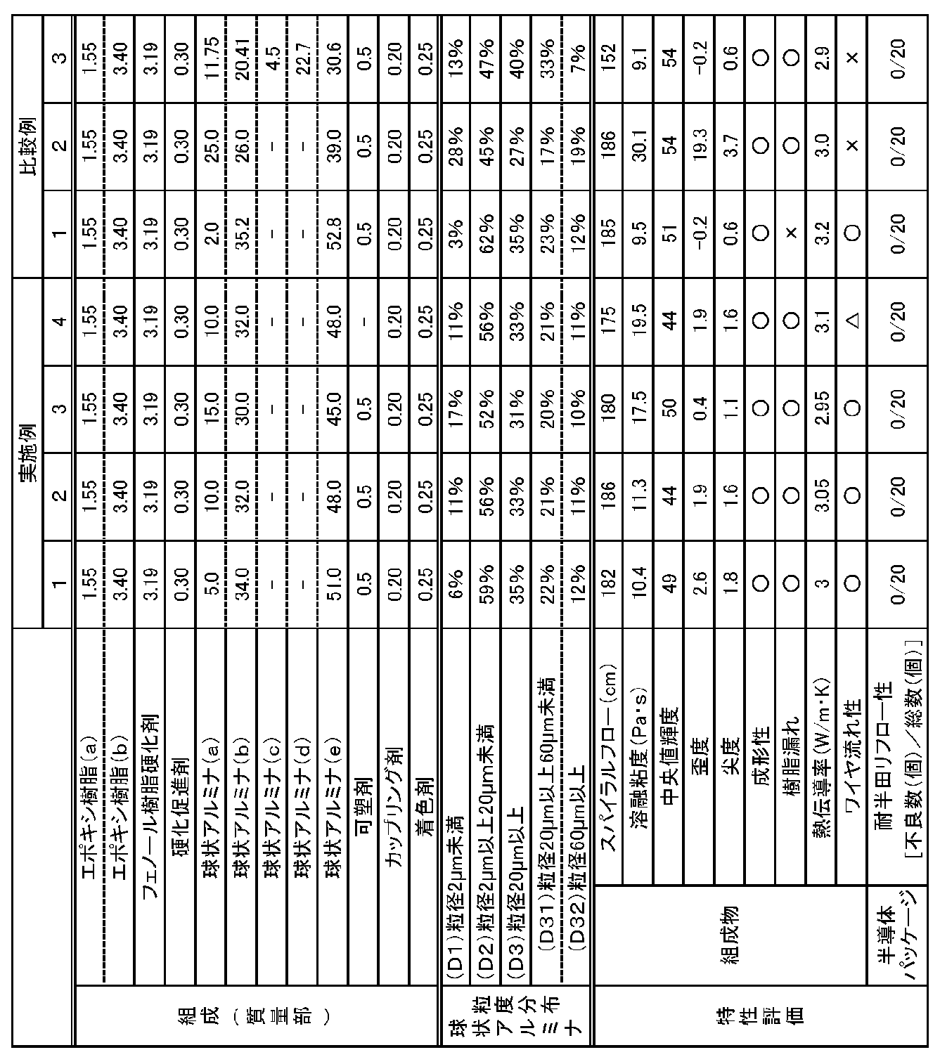
(実施例2〜4、比較例1〜3)
組成を表2に示すように変えた以外は、実施例1と同様にして粉粒状半導体封止用樹脂組成物を得た。
(Examples 2-4, Comparative Examples 1-3)
A resin composition for encapsulating a granular semiconductor was obtained in the same manner as in Example 1 except that the composition was changed as shown in Table 2.
上記各実施例及び各比較例で得られた粉粒状半導体封止用樹脂組成物について、下記に示す方法で各種特性を評価した。 Various characteristics of the resin composition for encapsulating a granular semiconductor obtained in each of the above Examples and Comparative Examples were evaluated by the methods described below.
<粉粒状半導体封止用樹脂組成物>
(1)スパイラルフロー
半導体封止用樹脂組成物を温度175℃及び圧力9.8MPaの条件でトランスファー成形し、測定した。
(2)溶融粘度
高化式フローテスタ((株)島津製作所製 CFT−500C)を用い、ノズル長1.0mm、ノズル径0.5mm、温度175℃、荷重圧力10kgf/cm2(約0.98MPa)の条件で測定した。
(3)融け性(中央値輝度、歪度、尖度)
半導体封止用樹脂組成物5gを直径50mmのアルミカップに入れ、175℃のオーブンにて10分間加熱溶融させた後、溶融した樹脂組成物の中央部直径約42mm(1+2/3インチ)を300dpiの解像度でカラー撮像して、直径500pixelの円の輝度情報を取得した。
さらに、演算処理により、歪度および尖度を求めた。
(4)成形性
半導体封止用樹脂組成物を用いて、FBGAパッケージ(50mm×50mm×0.54mm)を、175℃で、2分間の条件で圧縮成形した後、成形物の表面における外観異常(「巣」またはボイド)の発生を観察し、下記の基準で評価した。
○:外観異常なし(良好)
×:外観異常あり(不良)
(5)樹脂漏れ
半導体封止用樹脂組成物を用いて、FBGAパッケージ(50mm×50mm×0.54mm)を、175℃で、2分間の条件で圧縮成形した後、金型周辺部への樹脂漏れ(飛散)の有無を観察し、下記の基準で評価した。
○:樹脂漏れなし(良好)
×:樹脂漏れあり(不良)
(6)熱伝導率
半導体封止用樹脂組成物を175℃、10分間の条件でトランスファー成形して作製した円盤状試験片(直径100mm、厚さ26mm)について、迅速熱伝導率計(京都電子工業(株)製 製品名 Kemtherm QTM−3)を用いて測定した。
(7)ワイヤ流れ性
半導体封止用樹脂組成物を用いて、175℃、2分間および175℃×8時間の条件でFBGAパッケージ(50mm×50mm×0.54mm)を成形した後、X線検査装置(ポニー工業(株)製)によりワイヤの変形を観察し、最大変形部のワイヤ流れ率を測定し、下記の基準で評価した。
○:ワイヤ流れ率3%未満(良好)
×:ワイヤ流れ率3%以上(不良)
<Powdered semiconductor sealing resin composition>
(1) Spiral flow The semiconductor sealing resin composition was measured by transfer molding under conditions of a temperature of 175 ° C. and a pressure of 9.8 MPa.
(2) Melt viscosity Using a Koka flow tester (CFT-500C manufactured by Shimadzu Corporation), a nozzle length of 1.0 mm, a nozzle diameter of 0.5 mm, a temperature of 175 ° C., and a load pressure of 10 kgf / cm 2 (about 0. 98 MPa).
(3) Meltability (median brightness, skewness, kurtosis)
5 g of a semiconductor sealing resin composition is put in an aluminum cup having a diameter of 50 mm and heated and melted in an oven at 175 ° C. for 10 minutes, and then the center diameter of the melted resin composition is about 42 mm (1 + 2/3 inch) at 300 dpi. The luminance information of a circle having a diameter of 500 pixels was obtained by performing color imaging at a resolution of.
Further, the skewness and kurtosis were obtained by arithmetic processing.
(4) Formability After an FBGA package (50 mm × 50 mm × 0.54 mm) is compression molded at 175 ° C. for 2 minutes using the resin composition for semiconductor encapsulation, the appearance abnormality on the surface of the molded product The occurrence of (“nest” or void) was observed and evaluated according to the following criteria.
○: No abnormal appearance (good)
×: Appearance abnormality (defect)
(5) Resin leakage After compression molding of an FBGA package (50 mm x 50 mm x 0.54 mm) at 175 ° C for 2 minutes using a resin composition for semiconductor encapsulation, resin to the mold periphery The presence or absence of leakage (scattering) was observed and evaluated according to the following criteria.
○: No resin leakage (good)
×: Resin leakage (defect)
(6) Thermal conductivity Rapid thermal conductivity meter (Kyoto Electronics) for disk-shaped test pieces (diameter: 100 mm, thickness: 26 mm) produced by transfer molding of a semiconductor sealing resin composition at 175 ° C. for 10 minutes. Measurement was performed using a product name Kemtherm QTM-3 manufactured by Kogyo Co., Ltd.
(7) Wire flowability After forming an FBGA package (50 mm × 50 mm × 0.54 mm) under the conditions of 175 ° C., 2 minutes and 175 ° C. × 8 hours using the resin composition for semiconductor encapsulation, X-ray inspection The deformation of the wire was observed with a device (manufactured by Pony Industry Co., Ltd.), the wire flow rate of the maximum deformation portion was measured, and evaluated according to the following criteria.
○: Wire flow rate of less than 3% (good)
×: Wire flow rate of 3% or more (defect)
<半導体パッケージ>
(1)耐半田リフロー性
上記(7)で作製したFBGAパッケージに、30℃、60%RH、192時間の吸湿処理を施した後、IRリフロー処理(260℃、10秒)を行い、パッケージの内部クラック(剥離)の発生の有無を超音波探傷装置(SAT)で観察し、その発生率(不良数(個)/総数(個))を調べた(n=20)。
<Semiconductor package>
(1) Solder reflow resistance After subjecting the FBGA package produced in (7) above to moisture absorption treatment at 30 ° C., 60% RH, 192 hours, IR reflow treatment (260 ° C., 10 seconds) is performed, and the package The occurrence of internal cracks (peeling) was observed with an ultrasonic flaw detector (SAT), and the occurrence rate (number of defects (number) / total number (number)) was examined (n = 20).
上記結果を表2下欄に示した。なお、表2には半導体封止用樹脂組成物中の調製に使用した球状アルミナ(複数種の球状アルミナの混合物)の粒度分布を併せ示した。この粒度分布は、レーザ回折式粒度分布測定装置((株)島津製作所製のSALD−2200)を用いて測定し、(D1)粒径が2μm未満の粒子、(D2)粒径が2μm以上20μm以下の粒子、(D3)粒径が20μmを超える粒子の含有割合を質量基準で求めたものである。(D3)粒径が20μmを超える粒子については、さらに(D31)粒径が20μm以上60μm未満の粒子、および(D32)粒径60μm以上の粒子の含有割合をそれぞれ求めた。 The results are shown in the lower column of Table 2. Table 2 also shows the particle size distribution of spherical alumina (mixture of plural kinds of spherical alumina) used for preparation in the resin composition for semiconductor encapsulation. This particle size distribution is measured using a laser diffraction particle size distribution measuring apparatus (SALD-2200 manufactured by Shimadzu Corporation). (D1) Particles having a particle size of less than 2 μm, (D2) Particle sizes of 2 μm or more and 20 μm The content ratio of the following particles, (D3) particles having a particle diameter exceeding 20 μm, is determined on a mass basis. (D3) About the particle | grains with a particle size exceeding 20 micrometers, the content rate of (D31) particle | grains whose particle diameter is 20 micrometers or more and less than 60 micrometers and (D32) particle diameter of 60 micrometers or more was calculated | required, respectively.
以上より、本発明の粉粒状半導体封止用エポキシ樹脂組成物は、圧縮成形時の融け性および流動性を適正な範囲とすることができるため、ワイヤ流れや樹脂の漏れの問題がなく、かつ熱伝導性に優れたものとなることがわかった。 As mentioned above, since the epoxy resin composition for granular semiconductor encapsulation of the present invention can make the meltability and fluidity during compression molding within an appropriate range, there is no problem of wire flow or resin leakage, and It was found that the thermal conductivity was excellent.
Claims (6)
前記(D)球状アルミナは、該樹脂組成物中に80質量%以上95質量%未満含まれるとともに、(D1)粒径2μm未満の球状アルミナを5〜25質量%含有することを特徴とする粉粒状半導体封止用樹脂組成物。 (A) An epoxy resin, (B) a phenol resin curing agent, (C) a curing accelerator, and (D) a granular semiconductor sealing resin composition containing spherical alumina,
The (D) spherical alumina is contained in the resin composition in an amount of 80% by mass or more and less than 95% by mass, and (D1) a powder containing 5 to 25% by mass of spherical alumina having a particle size of less than 2 μm. Granular semiconductor encapsulating resin composition.
Priority Applications (1)
| Application Number | Priority Date | Filing Date | Title |
|---|---|---|---|
| JP2016081866A JP6712895B2 (en) | 2016-04-15 | 2016-04-15 | Powder-granular resin composition for semiconductor encapsulation and semiconductor device |
Applications Claiming Priority (1)
| Application Number | Priority Date | Filing Date | Title |
|---|---|---|---|
| JP2016081866A JP6712895B2 (en) | 2016-04-15 | 2016-04-15 | Powder-granular resin composition for semiconductor encapsulation and semiconductor device |
Publications (2)
| Publication Number | Publication Date |
|---|---|
| JP2017190425A true JP2017190425A (en) | 2017-10-19 |
| JP6712895B2 JP6712895B2 (en) | 2020-06-24 |
Family
ID=60085612
Family Applications (1)
| Application Number | Title | Priority Date | Filing Date |
|---|---|---|---|
| JP2016081866A Active JP6712895B2 (en) | 2016-04-15 | 2016-04-15 | Powder-granular resin composition for semiconductor encapsulation and semiconductor device |
Country Status (1)
| Country | Link |
|---|---|
| JP (1) | JP6712895B2 (en) |
Cited By (5)
| Publication number | Priority date | Publication date | Assignee | Title |
|---|---|---|---|---|
| WO2019131097A1 (en) * | 2017-12-28 | 2019-07-04 | 日立化成株式会社 | Encapsulating epoxy resin composition for ball grid array package, cured epoxy resin object, and electronic component/device |
| KR20200094221A (en) * | 2017-12-28 | 2020-08-06 | 히타치가세이가부시끼가이샤 | Epoxy resin composition for sealing a ball grid array package, cured epoxy resin, and electronic component device |
| CN111527147A (en) * | 2017-12-28 | 2020-08-11 | 日立化成株式会社 | Epoxy resin composition for ball grid array encapsulation, epoxy resin cured product and electronic component device |
| JP2023519137A (en) * | 2020-03-26 | 2023-05-10 | ディディピー スペシャルティ エレクトロニック マテリアルズ ユーエス,エルエルシー | Thermal Interface Materials Containing Spherical Fillers with Multimodal Distribution |
| WO2024190577A1 (en) * | 2023-03-10 | 2024-09-19 | 京セラ株式会社 | Epoxy resin composition and semiconductor device |
Citations (6)
| Publication number | Priority date | Publication date | Assignee | Title |
|---|---|---|---|---|
| JPH07278415A (en) * | 1994-04-13 | 1995-10-24 | Shin Etsu Chem Co Ltd | Resin composition for semiconductor encapsulation and semiconductor device |
| JPH11269352A (en) * | 1998-03-23 | 1999-10-05 | Nitto Denko Corp | Epoxy resin composition for semiconductor encapsulation |
| JP2005290076A (en) * | 2004-03-31 | 2005-10-20 | Sumitomo Bakelite Co Ltd | Epoxy resin composition and semiconductor device |
| JP2007262398A (en) * | 2006-03-01 | 2007-10-11 | Hitachi Chem Co Ltd | Epoxy resin composition and electronic component device |
| JP2008001748A (en) * | 2006-06-20 | 2008-01-10 | Kyocera Chemical Corp | Epoxy resin composition for sealing and semiconductor device |
| JP2010024464A (en) * | 2009-11-04 | 2010-02-04 | Sumitomo Bakelite Co Ltd | Epoxy resin composition and semiconductor device |
-
2016
- 2016-04-15 JP JP2016081866A patent/JP6712895B2/en active Active
Patent Citations (6)
| Publication number | Priority date | Publication date | Assignee | Title |
|---|---|---|---|---|
| JPH07278415A (en) * | 1994-04-13 | 1995-10-24 | Shin Etsu Chem Co Ltd | Resin composition for semiconductor encapsulation and semiconductor device |
| JPH11269352A (en) * | 1998-03-23 | 1999-10-05 | Nitto Denko Corp | Epoxy resin composition for semiconductor encapsulation |
| JP2005290076A (en) * | 2004-03-31 | 2005-10-20 | Sumitomo Bakelite Co Ltd | Epoxy resin composition and semiconductor device |
| JP2007262398A (en) * | 2006-03-01 | 2007-10-11 | Hitachi Chem Co Ltd | Epoxy resin composition and electronic component device |
| JP2008001748A (en) * | 2006-06-20 | 2008-01-10 | Kyocera Chemical Corp | Epoxy resin composition for sealing and semiconductor device |
| JP2010024464A (en) * | 2009-11-04 | 2010-02-04 | Sumitomo Bakelite Co Ltd | Epoxy resin composition and semiconductor device |
Cited By (13)
| Publication number | Priority date | Publication date | Assignee | Title |
|---|---|---|---|---|
| CN111527146B (en) * | 2017-12-28 | 2024-03-01 | 株式会社力森诺科 | Epoxy resin composition, epoxy resin cured product and electronic component device for ball grid array packaging sealing |
| KR20200094221A (en) * | 2017-12-28 | 2020-08-06 | 히타치가세이가부시끼가이샤 | Epoxy resin composition for sealing a ball grid array package, cured epoxy resin, and electronic component device |
| CN111527147A (en) * | 2017-12-28 | 2020-08-11 | 日立化成株式会社 | Epoxy resin composition for ball grid array encapsulation, epoxy resin cured product and electronic component device |
| CN111527144A (en) * | 2017-12-28 | 2020-08-11 | 日立化成株式会社 | Epoxy resin composition for ball grid array encapsulation, epoxy resin cured product and electronic component device |
| CN111527146A (en) * | 2017-12-28 | 2020-08-11 | 日立化成株式会社 | Epoxy resin composition for sealing ball grid array package, cured epoxy resin, and electronic component device |
| JPWO2019131097A1 (en) * | 2017-12-28 | 2020-12-17 | 昭和電工マテリアルズ株式会社 | Epoxy resin composition for sealing ball grid array packages, cured epoxy resin, and electronic component equipment |
| JP7276151B2 (en) | 2017-12-28 | 2023-05-18 | 株式会社レゾナック | EPOXY RESIN COMPOSITION FOR BALL GRID ARRAY PACKAGE SEALING, EPOXY RESIN CURED MATERIAL, AND ELECTRONIC PARTS DEVICE |
| TWI820067B (en) * | 2017-12-28 | 2023-11-01 | 日商力森諾科股份有限公司 | Epoxy resin composition for sealing ball grid array package, epoxy resin cured product and electronic component device |
| WO2019131097A1 (en) * | 2017-12-28 | 2019-07-04 | 日立化成株式会社 | Encapsulating epoxy resin composition for ball grid array package, cured epoxy resin object, and electronic component/device |
| KR102840984B1 (en) * | 2017-12-28 | 2025-07-30 | 가부시끼가이샤 레조낙 | Epoxy resin composition for sealing ball grid array packages, epoxy resin cured product and electronic component device |
| JP2023519137A (en) * | 2020-03-26 | 2023-05-10 | ディディピー スペシャルティ エレクトロニック マテリアルズ ユーエス,エルエルシー | Thermal Interface Materials Containing Spherical Fillers with Multimodal Distribution |
| WO2024190577A1 (en) * | 2023-03-10 | 2024-09-19 | 京セラ株式会社 | Epoxy resin composition and semiconductor device |
| TWI898472B (en) * | 2023-03-10 | 2025-09-21 | 日商京瓷股份有限公司 | Epoxy resin composition and semiconductor device |
Also Published As
| Publication number | Publication date |
|---|---|
| JP6712895B2 (en) | 2020-06-24 |
Similar Documents
| Publication | Publication Date | Title |
|---|---|---|
| JP6968001B2 (en) | Resin composition and semiconductor device for semiconductor encapsulation for transfer compression molding method | |
| JP6832193B2 (en) | Resin composition and resin-sealed semiconductor device | |
| JP2017190425A (en) | Granular resin composition for semiconductor sealing and semiconductor device | |
| EP3029083A1 (en) | Resin composition for semiconductor encapsulation and semiconductor encapsulation method using same | |
| JP6107013B2 (en) | Epoxy resin composition for semiconductor encapsulation and semiconductor device using the same | |
| JP5189606B2 (en) | Epoxy resin composition for semiconductor encapsulation, and semiconductor device | |
| JP2019044006A (en) | Resin composition for semiconductor sealing and semiconductor device | |
| JP6389382B2 (en) | Semiconductor encapsulating resin sheet and resin encapsulating semiconductor device | |
| JP2009275146A (en) | Epoxy resin composition for sealing semiconductor and semiconductor device using the same | |
| JP2019176023A (en) | Semiconductor-sealing resin composition and semiconductor device | |
| CN105551980B (en) | The preparation method of semiconductor device | |
| JP2014118461A (en) | Resin composition for granular semiconductor sealing and semiconductor device | |
| WO2019131097A1 (en) | Encapsulating epoxy resin composition for ball grid array package, cured epoxy resin object, and electronic component/device | |
| JP5349087B2 (en) | Epoxy resin composition for sealing optical semiconductor light receiving element, method for producing the same, and optical semiconductor device | |
| JP6276365B2 (en) | Method for evaluating meltability of resin composition for encapsulating powdery semiconductor and method for producing resin-encapsulated semiconductor device | |
| JP6981024B2 (en) | Encapsulating resin composition and semiconductor device | |
| JPH107888A (en) | Epoxy resin composition for semiconductor encapsulation | |
| JP7002866B2 (en) | Resin composition for encapsulating powdered and granular semiconductors and semiconductor devices | |
| TWI796507B (en) | Resin composition for sheet-like sealing, and semiconductor device | |
| KR20130074664A (en) | Epoxy resin composition for encapsulating semiconductor device, and semiconductor apparatus using the same | |
| JP2007217469A (en) | Epoxy resin composition for sealing and semiconductor device | |
| JP4567641B2 (en) | Epoxy resin composition for sealing semiconductor element and semiconductor element using the same | |
| JP6351927B2 (en) | Resin composition for sealing and method for manufacturing semiconductor device | |
| JP2006265487A (en) | Epoxy resin composition for sealing semiconductor | |
| JP2523669B2 (en) | Semiconductor device |
Legal Events
| Date | Code | Title | Description |
|---|---|---|---|
| A621 | Written request for application examination |
Free format text: JAPANESE INTERMEDIATE CODE: A621 Effective date: 20181113 |
|
| A977 | Report on retrieval |
Free format text: JAPANESE INTERMEDIATE CODE: A971007 Effective date: 20190821 |
|
| A131 | Notification of reasons for refusal |
Free format text: JAPANESE INTERMEDIATE CODE: A131 Effective date: 20190903 |
|
| A521 | Request for written amendment filed |
Free format text: JAPANESE INTERMEDIATE CODE: A523 Effective date: 20191101 |
|
| A131 | Notification of reasons for refusal |
Free format text: JAPANESE INTERMEDIATE CODE: A131 Effective date: 20191203 |
|
| A521 | Request for written amendment filed |
Free format text: JAPANESE INTERMEDIATE CODE: A523 Effective date: 20200130 |
|
| TRDD | Decision of grant or rejection written | ||
| A01 | Written decision to grant a patent or to grant a registration (utility model) |
Free format text: JAPANESE INTERMEDIATE CODE: A01 Effective date: 20200512 |
|
| A61 | First payment of annual fees (during grant procedure) |
Free format text: JAPANESE INTERMEDIATE CODE: A61 Effective date: 20200602 |
|
| R150 | Certificate of patent or registration of utility model |
Ref document number: 6712895 Country of ref document: JP Free format text: JAPANESE INTERMEDIATE CODE: R150 |