JP2017191155A - Display device - Google Patents
Display device Download PDFInfo
- Publication number
- JP2017191155A JP2017191155A JP2016079362A JP2016079362A JP2017191155A JP 2017191155 A JP2017191155 A JP 2017191155A JP 2016079362 A JP2016079362 A JP 2016079362A JP 2016079362 A JP2016079362 A JP 2016079362A JP 2017191155 A JP2017191155 A JP 2017191155A
- Authority
- JP
- Japan
- Prior art keywords
- electrode
- display device
- disposed
- signal line
- insulating film
- Prior art date
- Legal status (The legal status is an assumption and is not a legal conclusion. Google has not performed a legal analysis and makes no representation as to the accuracy of the status listed.)
- Pending
Links
Images




Landscapes
- Liquid Crystal (AREA)
Abstract
【課題】液晶セルに直流が印加されることがあり、このとき、配向膜に電荷が蓄積される。【解決手段】表示装置は、アレイ基板と、対向基板と、を備える。アレイ基板は、映像信号線と、走査信号線と、共通電極と、画素電極と、共通電極と画素電極との間に配置される絶縁膜と、絶縁膜の上に形成される突起部と、突起部の上に形成される電極と、画素電極、絶縁膜および電極の上に形成される配向膜と、を備える。その電極は画素電極と異なる電位が供給される。【選択図】図1A direct current may be applied to a liquid crystal cell, and at this time, charges are accumulated in an alignment film. A display device includes an array substrate and a counter substrate. The array substrate includes a video signal line, a scanning signal line, a common electrode, a pixel electrode, an insulating film disposed between the common electrode and the pixel electrode, and a protrusion formed on the insulating film, An electrode formed on the protrusion, and an alignment film formed on the pixel electrode, the insulating film, and the electrode. A potential different from that of the pixel electrode is supplied to the electrode. [Selection] Figure 1
Description
本開示は表示装置に関し、例えば電荷除去部を備える液晶表示装置に適用可能である。 The present disclosure relates to a display device, and can be applied to, for example, a liquid crystal display device including a charge removing unit.
液晶表示では直流駆動すると寿命が短くなるため、交流電圧を加えることで駆動する交流電圧駆動が行われている。交流による駆動電圧はプラスとマイナスの両電圧が総体として等しくなるように印加されなければならない。 In the liquid crystal display, when the DC driving is performed, the life is shortened. Therefore, the AC voltage driving is performed by applying the AC voltage. The drive voltage by alternating current must be applied so that both positive and negative voltages are equal.
液晶セルに交流電圧を印加した際に、突抜電極の調整ずれなどの影響で液晶セルに直流が印加される。このとき、配向膜に電荷が蓄積され、液晶層に印加される交流電圧が正極と負極で非対称となり、フリッカが生じる。
本開示の課題は、配向膜に蓄積される電荷を低減する表示装置を提供することにある。
その他の課題と新規な特徴は、本開示の記述および添付図面から明らかになるであろう。
When an alternating voltage is applied to the liquid crystal cell, a direct current is applied to the liquid crystal cell due to the effect of misalignment of the punch electrode. At this time, charges are accumulated in the alignment film, and the alternating voltage applied to the liquid crystal layer becomes asymmetric between the positive electrode and the negative electrode, causing flicker.
An object of the present disclosure is to provide a display device that reduces charges accumulated in an alignment film.
Other problems and novel features will become apparent from the description of the present disclosure and the accompanying drawings.
本開示のうち、代表的なものの概要を簡単に説明すれば、下記のとおりである。
すなわち、表示装置は、アレイ基板と、対向基板と、を備える。前記アレイ基板は、映像信号線と、走査信号線と、共通電極と、画素電極と、前記共通電極と前記画素電極との間に配置される絶縁膜と、前記絶縁膜の上に形成される突起部と、前記突起部の上に形成される電極と、前記画素電極、前記絶縁膜および前記電極の上に形成される配向膜と、を備える。前記電極は前記画素電極と異なる電位が供給される。
The outline of a representative one of the present disclosure will be briefly described as follows.
That is, the display device includes an array substrate and a counter substrate. The array substrate is formed on the insulating film and a video signal line, a scanning signal line, a common electrode, a pixel electrode, an insulating film disposed between the common electrode and the pixel electrode. A protrusion, an electrode formed on the protrusion, and an alignment film formed on the pixel electrode, the insulating film, and the electrode. The electrode is supplied with a potential different from that of the pixel electrode.
以下に、実施形態、実施例および変形例について、図面を参照しつつ説明する。なお、開示はあくまで一例にすぎず、当業者において、発明の主旨を保っての適宜変更について容易に想到し得るものについては、当然に本発明の範囲に含有されるものである。また、図面は説明をより明確にするため、実際の態様に比べ、各部の幅、厚さ、形状等について模式的に表される場合があるが、あくまで一例であって、本発明の解釈を限定するものではない。また、本明細書と各図において、既出の図に関して前述したものと同様の要素には、同一の符号を付して、詳細な説明を適宜省略することがある。 Embodiments, examples, and modifications will be described below with reference to the drawings. It should be noted that the disclosure is merely an example, and those skilled in the art can easily conceive of appropriate modifications while maintaining the gist of the invention are naturally included in the scope of the present invention. In addition, the drawings may be schematically represented with respect to the width, thickness, shape, and the like of each part in comparison with actual aspects for the sake of clarity of explanation, but are merely examples, and the interpretation of the present invention is not limited. It is not limited. In addition, in the present specification and each drawing, elements similar to those described above with reference to the previous drawings are denoted by the same reference numerals, and detailed description may be omitted as appropriate.
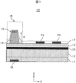
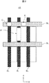
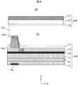
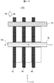
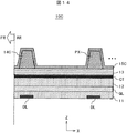
実施形態に係る表示装置のアレイ基板について図1、2を用いて説明する。図1は実施形態に係る表示装置のアレイ基板の断面図である。図2は図1の平面図である。以下、+Z方向を上、−Z方向を下という。 The array substrate of the display device according to the embodiment will be described with reference to FIGS. FIG. 1 is a cross-sectional view of an array substrate of a display device according to an embodiment. FIG. 2 is a plan view of FIG. Hereinafter, the + Z direction is referred to as “up” and the −Z direction is referred to as “down”.
実施形態に係るアレイ基板10は、映像信号線DLの上に配置される絶縁膜11と、絶縁膜11の上に配置される、図1には図示されない走査信号線GLと、走査信号線GLの上に配置される有機膜12と、有機膜12の上に配置される共通電極CTと、共通電極CTの上に配置される絶縁膜13と、絶縁膜13の上に配置される画素電極PXと、を備える。アレイ基板10は、さらに、絶縁膜13の上に配置される突起部14と突起部14の上に配置される電極15とで構成される電荷除去部16と、絶縁膜13と画素電極PXと電荷除去部16との上に配置される配向膜17とを備える。突起部14は絶縁膜13からH以上の高さを有し、その上に配置された電極15には、画素電極PXとは異なる電位が供給される。
The
電荷除去部16の電極15と画素電極PXとは異なる電位が供給されるため、配向膜17上に溜まった電荷は拡散と電位勾配により移動する。これにより、フリッカを低減することができる。仮に電極15と画素電極PXが同電位であると配向膜17に溜まった電荷の逃げ道がないので電荷は滞留する。
Since different potentials are supplied to the
図2に示すように、電荷除去部16は映像信号線DL上(A領域)でも、走査信号線GL上(B領域)でも、映像信号線DLと走査信号線GLの交差部(C領域)でも、どこにあっても良いが、表示領域ARの遮光層の配置される領域に配置するのが好ましい。1画素あたり1個でなくともよく、表示領域AR面内に複数個あれば良い。
As shown in FIG. 2, the
実施形態に係る表示装置は、蓄積された電荷を除去するための構造をセル内に設ける。配向膜直下に電極を設けることで、電荷の抜け道とする。また電荷を抜けやすくするため配向膜厚を薄くし抵抗値を下げる。このため、電荷除去部の電極は、遮光層の開口部に位置する画素電極よりも高い位置に存在する。 In the display device according to the embodiment, a structure for removing the accumulated electric charge is provided in the cell. By providing an electrode directly under the alignment film, it becomes a passage for electric charge. In addition, the thickness of the alignment film is reduced to reduce the resistance value in order to facilitate the removal of charges. For this reason, the electrode of the charge removal unit exists at a position higher than the pixel electrode located in the opening of the light shielding layer.
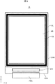
図3は実施例1の表示装置の全体構成を説明するための平面図である。図4は画素の等価回路図である。実施例1の表示装置1Aは、画素電極PXや薄膜トランジスタTFT等が形成されるアレイ基板10Aと、アレイ基板10A対向して配置され色層(例えばカラーフィルタ)22等が形成される対向基板20Aと、アレイ基板10Aと対向基板20Aとで挟持される液晶層30と、光源となる図示しないバックライトユニット(バックライト装置)と、を備える。アレイ基板10Aと対向基板20Aとの固定及び液晶の封止は、対向基板20Aの周辺部の額縁領域FRに環状に塗布されたシール材SLで固定され、液晶も封止される構成となっている。ただし、表示装置1では、液晶が封入された領域の内で表示画素(以下、画素と略記する)の形成される領域が表示領域ARとなる。従って、液晶が封入されている領域内であっても、画素が形成されておらず表示に係わらない領域は表示領域ARとはならない。
FIG. 3 is a plan view for explaining the overall configuration of the display device according to the first embodiment. FIG. 4 is an equivalent circuit diagram of the pixel. The display device 1A according to the first embodiment includes an
また、対向基板20Aはアレイ基板10Aよりも小さな面積となっており、アレイ基板10Aの図中下側の辺部を露出させるようになっている。アレイ基板10Aの辺部には、半導体チップで構成される駆動回路DRが搭載されている。駆動回路DRは、表示領域ARに配置される各画素を駆動する。また、アレイ基板10Aおよび対向基板20Aとしては、例えば周知のガラス基板が基材として用いられるのが一般的であるが、樹脂性の透明絶縁基板であってもよい。
Further, the
表示装置1Aでは、アレイ基板10あの液晶側の面であって表示領域AR内には、図3中X方向に延在しY方向に並設され、駆動回路DRからの走査信号が供給される走査信号線(ゲート線)GLが形成されている。また、図3中Y方向に延在しX方向に並設され、駆動回路DRからの映像信号(階調信号)が供給される映像信号線(ドレイン線)DLが形成されている。隣接する2本のドレイン線DLと隣接する2本のゲート線GLとで囲まれる領域が画素を構成し、複数の画素が、ドレイン線DLおよびゲート線GLに沿って、表示領域AR内においてマトリックス状に配置されている。
In the display device 1A, the surface of the
各画素は、例えば、図4に示すように、ゲート線GLからの走査信号によってオン/オフ駆動される薄膜トランジスタTFTと、このオンされた薄膜トランジスタTFTを介してドレイン線DLからの映像信号が供給される壁状の画素電極PXと、コモン線CLを介して映像信号の電位に対して基準となる電位を有する共通信号が供給される壁状の共通電極CTとを備えている。図4においては、画素電極PXおよび共通電極CTを模式的に線状に記しているが、画素電極PXおよび共通電極CTの構成については、後に詳述する。なお、薄膜トランジスタTFTは、そのバイアスの印加によってドレイン電極とソース電極が入れ替わるように駆動するが、本明細書中においては、便宜上、ドレイン線DLと接続される側をドレイン電極、壁画素電極PXと接続される側をソース電極と記す。 For example, as shown in FIG. 4, each pixel is supplied with a thin film transistor TFT that is turned on / off by a scanning signal from the gate line GL and a video signal from the drain line DL through the turned on thin film transistor TFT. A wall-like pixel electrode PX and a wall-like common electrode CT to which a common signal having a reference potential with respect to the potential of the video signal is supplied via the common line CL. In FIG. 4, the pixel electrode PX and the common electrode CT are schematically illustrated in a linear shape, but the configuration of the pixel electrode PX and the common electrode CT will be described in detail later. Note that the thin film transistor TFT is driven so that the drain electrode and the source electrode are switched by application of the bias. However, for the sake of convenience, the side connected to the drain line DL is referred to as the drain electrode and the wall pixel electrode PX. The connected side is referred to as a source electrode.
各ドレイン線DLおよび各ゲート線GLはその端部においてシール材SLを越えてそれぞれ延在され、外部システムからフレキシブルプリント基板FPCを介して入力される入力信号に基づいて、映像信号や走査信号等の駆動信号を生成する駆動回路DRに接続される。ただし、表示装置1では、走査線の駆動信号を生成する走査信号駆動回路を半導体チップで形成した駆動回路DRをアレイ基板10に搭載する構成としているが、走査信号駆動回路をアレイ基板10Aの額縁領域にTFT等で形成する構成であってもよい。
Each drain line DL and each gate line GL extend beyond the sealing material SL at their ends, and based on an input signal input from an external system through the flexible printed circuit board FPC, a video signal, a scanning signal, etc. Is connected to a drive circuit DR that generates a drive signal. However, in the
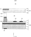
実施例1は電荷除去部を映像信号線上(A領域)に配置する例であり、これについて図5、6を用いて説明する。図5は実施例1に係る表示装置の構成を示す平面図である。図6は図5のA−A’線における断面図である。 The first embodiment is an example in which the charge removing unit is disposed on the video signal line (A region), and this will be described with reference to FIGS. FIG. 5 is a plan view illustrating the configuration of the display device according to the first embodiment. 6 is a cross-sectional view taken along the line A-A 'of FIG.
アレイ基板10Aは、図示しないガラス基板の上に配置される映像信号線DLと、映像信号線DLの上に配置される絶縁膜11と、絶縁膜11の上に配置される、図6には図示されない走査信号線GLと、走査信号線GLの上に配置される有機膜12と、有機膜12の上に配置される共通電極CTと、共通電極CTの上に配置される絶縁膜13と、絶縁膜13の上に配置される画素電極PXと、を備える。アレイ基板10Aは、さらに、映像信号線DLの上方であって絶縁膜13の上に配置される突起部14Aと突起部14Aの上に配置される電極15Aとで構成される電荷除去部16Aと、絶縁膜13と画素電極PXと電荷除去部16Aとの上に配置される配向膜17とを備える。突起部14Aは絶縁膜13からH以上の高さを有し、その上に配置された電極15Aには、画素電極PXとは異なる電位が供給される。例えば、突起部14Aの高さが0.5μm以上(H≧0.5μm)になることにより配向膜17の厚みが50nm以下となる。電極15上部の配向膜17の薄膜化により配向膜17の抵抗が低下し、蓄積された電荷が電極15Aから除去されやすくなる。例えば、電極15Aは後述する実施例2と同様に共通電極CTに接続される。
The
対向基板20Aは、図示しないガラス基板の下に配置される遮光層21と、遮光層21の開口部に配置される色層22と、遮光層21と色層22との下に配置されるオーバコート層23と、オーバコート層23の下に配置される配向膜24と、を備える。アレイ基板10Aの突起部14A上の配向膜17と対向基板20A側の配向膜24は接触してもよいし、接触しなくともよい。なお、対向基板20Aには実施例2において後述する突起部25と同様な突起部を備えてもよい。
The
実施例2は映像信号線と走査信号線との交差部の上に電荷除去部を配置する例であり、これについて図7、8を用いて説明する。図7は実施例2に係る表示装置の構成を示す平面図である。図8は図7のA−A’線における断面図である。 The second embodiment is an example in which a charge removing unit is disposed on an intersection between a video signal line and a scanning signal line. This will be described with reference to FIGS. FIG. 7 is a plan view illustrating the configuration of the display device according to the second embodiment. FIG. 8 is a cross-sectional view taken along line A-A ′ of FIG. 7.
実施例2に係る表示装置1Bのアレイ基板10Bは、電荷除去部の位置および形状を除いて、実施例1に係るアレイ基板10Aと同様な構造である。実施例2に係る対向基板20Bは実施例1に係る対向基板20Aと同様な構造である。
The
アレイ基板10Bは、図示しないガラス基板の上に配置される映像信号線DLと、映像信号線DLの上に配置される絶縁膜11と、絶縁膜11の上に配置される走査信号線GLと、走査信号線GLの上に配置される有機膜12と、有機膜12の上に配置される共通電極CTと、共通電極CTの上に配置される絶縁膜13と、絶縁膜13の上に配置される画素電極PXと、を備える。アレイ基板10Bは、さらに、映像信号線DLと走査信号線GLとの交差部であって絶縁膜13の上に配置される突起部14Bと突起部14Bの上に配置される電極15Bとで構成される電荷除去部16Bと、絶縁膜13と画素電極PXと電荷除去部16Bとの上に配置される配向膜17とを備える。電極15Bは共通電極CTと接続され、画素電極PXと異なる電位が供給される。突起部14Bの高さは実施例1の突起部14Aと同様である。
The
アレイ基板10Bの突起部14B上の配向膜17と対向基板20側の配向膜24は接触するようにしてもよいし、接触しないようにしてもよい。また、アレイ基板10Bの突起部14B上の配向膜17と対向基板20B側の配向膜24と接触する場合、対向基板20B側に突起部25を設け突起部25の下の配向膜24と接触するようにしてもよい。
The
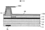
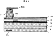
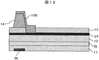
アレイ基板10Bの電極と共通電極を接続する製造方法について図9〜12を用いて説明する。図9は実施例2に係る表示装置のアレイ基板の製造方法の第1工程を示す断面図である。図10は実施例2に係る表示装置のアレイ基板の製造方法の第2工程を示す断面図である。図11は実施例2に係る表示装置のアレイ基板の製造方法の第3工程を示す断面図である。図12は実施例2に係る表示装置のアレイ基板の製造方法の第4工程を示す断面図である。
A manufacturing method for connecting the electrode of the
まず、図示しないガラス基板の上に金属を成膜して映像信号線DLを形成しと、映像信号線DLの上に絶縁膜11を形成し、絶縁膜11の上に金属を成膜し走査信号線GLを形成し、走査信号線GLの上に有機膜12を形成し、有機膜12の上にITOを成膜して共通電極CTを形成し、共通電極CTの上に絶縁膜13を形成する。
First, a metal film is formed on a glass substrate (not shown) to form a video signal line DL, an insulating
次に、図9に示すように、第1工程は、絶縁膜13の上に例えば有機膜を形成して突起部14Bを形成後、共通電極CTを露出するように絶縁膜13に孔を開けてコンタクトホールCNTを形成する。
Next, as shown in FIG. 9, in the first step, for example, an organic film is formed on the insulating
次に、図10に示すように、第1工程後、第2工程は全面にITOを成膜して、成膜したITOの上にレジスト膜を塗布する。 Next, as shown in FIG. 10, after the first step, in the second step, ITO is formed on the entire surface, and a resist film is applied on the formed ITO.
次に、図11に示すように、第2工程後、第3工程はフォトマスクを用いてレジストをパターニングする。 Next, as shown in FIG. 11, after the second step, in the third step, the resist is patterned using a photomask.
次に、図12に示すように、第3工程後、第4工程は残ったレジストをマスクにエッチングし、レジストを剥離して、共通電極CTと接続される電極15Bを形成する。このとき、画素電極PXを同時に形成するようにしてもよい。
Next, as shown in FIG. 12, after the third step, in the fourth step, the remaining resist is etched using the mask, and the resist is removed to form the
実施例3は映像信号線と走査信号線との交差部の上に突起部を配置し、走査信号線の上に電極を延在して電荷除去部を構成する例であり、これについて図13、14を用いて説明する。図13は実施例3に係る表示装置のアレイ基板の構成を示す平面図である。図14は図13のA−A’線における断面図である。 The third embodiment is an example in which a protrusion is disposed on an intersection between a video signal line and a scanning signal line, and an electrode is extended on the scanning signal line to form a charge removal unit. FIG. 14 will be described. FIG. 13 is a plan view illustrating the configuration of the array substrate of the display device according to the third embodiment. FIG. 14 is a cross-sectional view taken along the line A-A ′ of FIG. 13.
実施例3に係る表示装置のアレイ基板10Cは、電荷除去部の位置および電極が共通電極に接続されない点を除いて、実施例1のアレイ基板10と同様な構造である。実施例3に係る対向基板は実施例1の対向基板20Aと同様な構造である。
The array substrate 10C of the display device according to the third embodiment has the same structure as the
アレイ基板10Cは、図示しないガラス基板の上に配置される映像信号線DLと、映像信号線DLの上に配置される絶縁膜11と、絶縁膜11の上に配置される走査信号線GLと、走査信号線GLの上に配置される有機膜12と、有機膜12の上に配置される共通電極CTと、共通電極CTの上に配置される絶縁膜13と、絶縁膜13の上に配置される、図14では図示されない画素電極PXと、を備える。アレイ基板10Cは、さらに、絶縁膜13の上に配置される突起部14Cと突起部14Cの上に配置される電極15Cとで構成される電荷除去部16Cと、絶縁膜13と画素電極PXと電荷除去部16Cとの上に配置される配向膜17とを備える。突起部14Cは映像信号線DLと走査信号線GLとが交差部の上に走査信号線GLに沿って複数配置される。電極15Cは走査信号線GLの上に走査信号線GLに沿って延伸し、表示領域ARの外の額縁領域FRの図示しない配線に接続されて、画素電極の電位と異なる電位が供給される。突起部14Cの高さは実施例1の突起部14Aと同様である。
The array substrate 10C includes a video signal line DL disposed on a glass substrate (not shown), an insulating
アレイ基板10Cの突起部14C上の配向膜17と対向基板20側の配向膜は接触してもよいし、接触しなくともよい。なお、対向基板には実施例2の突起部25と同様な突起部を備えてもよい。
The
1A、1B、1C・・・表示装置
10、10A、10B、10C・・・アレイ基板
11・・・絶縁膜
12・・・有機膜
13・・・絶縁膜
14、14B、14C・・・突起部
15、15B、15C・・・電極
16、16B、16C・・・電荷除去部
17・・・配向膜
DL・・・映像信号線
CL・・・コモン線
CT・・・共通電極
PX・・・画素電極
20A、20B、20C・・・対向基板
21・・・遮光層
22・・・色層
23・・・オーバコート層
24・・・配向膜
25・・・突起部
1A, 1B, 1C ...
Claims (10)
アレイ基板と、
対向基板と、
を備え、
前記アレイ基板は、
映像信号線と、
走査信号線と、
共通電極と、
画素電極と、
前記共通電極と前記画素電極との間に配置される絶縁膜と、
前記絶縁膜の上に形成される突起部と、
前記突起部の上に形成される電極と、
前記画素電極、前記絶縁膜および前記電極の上に形成される配向膜と、
を備え、
前記電極は前記画素電極と異なる電位が供給される。 The display device
An array substrate;
A counter substrate;
With
The array substrate is
Video signal lines,
A scanning signal line;
A common electrode;
A pixel electrode;
An insulating film disposed between the common electrode and the pixel electrode;
A protrusion formed on the insulating film;
An electrode formed on the protrusion,
An alignment film formed on the pixel electrode, the insulating film, and the electrode;
With
The electrode is supplied with a potential different from that of the pixel electrode.
前記電極は前記共通電極に接続される。 The display device according to claim 1.
The electrode is connected to the common electrode.
前記電極は表示領域外に配置される配線に接続される。 The display device according to claim 1.
The electrodes are connected to wirings arranged outside the display area.
前記電極は前記映像信号線の上に配置される。 The display device according to claim 1.
The electrode is disposed on the video signal line.
前記電極は前記走査信号線の上に配置される。 The display device according to claim 1.
The electrode is disposed on the scanning signal line.
前記電極は前記映像信号線と前記走査信号線とが交差する部分の上に配置される。 The display device according to claim 1.
The electrode is disposed on a portion where the video signal line and the scanning signal line intersect.
前記突起部の高さは0.5μm以上である。 The display device according to claim 1.
The height of the protrusion is 0.5 μm or more.
対向基板は、
遮光層と、
色層と、
オーバコート膜と、
配向膜と、
を備える。 The display device according to claim 1.
The counter substrate is
A light shielding layer;
Color layers,
An overcoat film,
An alignment film;
Is provided.
前記電極の上の配向膜と前記対向基板の配向膜とが接触する。 The display device according to claim 8.
The alignment film on the electrode is in contact with the alignment film on the counter substrate.
前記対向基板は、さらに、突起部を備え、
前記電極は前記突起部と前記配向膜を介して接触する。 The display device according to claim 8.
The counter substrate further includes a protrusion,
The electrode is in contact with the protrusion through the alignment film.
Priority Applications (1)
| Application Number | Priority Date | Filing Date | Title |
|---|---|---|---|
| JP2016079362A JP2017191155A (en) | 2016-04-12 | 2016-04-12 | Display device |
Applications Claiming Priority (1)
| Application Number | Priority Date | Filing Date | Title |
|---|---|---|---|
| JP2016079362A JP2017191155A (en) | 2016-04-12 | 2016-04-12 | Display device |
Publications (1)
| Publication Number | Publication Date |
|---|---|
| JP2017191155A true JP2017191155A (en) | 2017-10-19 |
Family
ID=60085240
Family Applications (1)
| Application Number | Title | Priority Date | Filing Date |
|---|---|---|---|
| JP2016079362A Pending JP2017191155A (en) | 2016-04-12 | 2016-04-12 | Display device |
Country Status (1)
| Country | Link |
|---|---|
| JP (1) | JP2017191155A (en) |
Cited By (1)
| Publication number | Priority date | Publication date | Assignee | Title |
|---|---|---|---|---|
| CN116339002A (en) * | 2021-12-24 | 2023-06-27 | 夏普显示科技株式会社 | Liquid crystal panel |
-
2016
- 2016-04-12 JP JP2016079362A patent/JP2017191155A/en active Pending
Cited By (1)
| Publication number | Priority date | Publication date | Assignee | Title |
|---|---|---|---|---|
| CN116339002A (en) * | 2021-12-24 | 2023-06-27 | 夏普显示科技株式会社 | Liquid crystal panel |
Similar Documents
| Publication | Publication Date | Title |
|---|---|---|
| JP5114544B2 (en) | Display device | |
| JP5024110B2 (en) | Electro-optical device and electronic apparatus | |
| US9012898B2 (en) | Electrophoretic display | |
| JP5299224B2 (en) | Electro-optical device and electronic apparatus | |
| US9488887B2 (en) | Display device | |
| US8189159B2 (en) | Liquid crystal display device and method for manufacturing the same | |
| JP5199638B2 (en) | Liquid crystal display | |
| JP6218949B2 (en) | Active matrix substrate and liquid crystal panel | |
| CN106486494A (en) | Display device | |
| WO2016021319A1 (en) | Active matrix substrate, liquid crystal panel, and method for manufacturing active matrix substrate | |
| TWI534517B (en) | LCD panel | |
| CN112394586B (en) | Pixel structure | |
| JP6518327B2 (en) | Liquid crystal display and its array substrate | |
| JP2017076010A (en) | Display device | |
| JP5861740B2 (en) | Electro-optical device and electronic apparatus | |
| JP6164554B2 (en) | Display device | |
| JP5678992B2 (en) | Electro-optical device and electronic apparatus | |
| KR101227133B1 (en) | Liquid Crystal Display Panel Of Horizontal Electronic Fileld Applying Type | |
| JP6780062B2 (en) | Liquid crystal display device | |
| US10964251B2 (en) | Pixel array substrate and driving method thereof | |
| JP2019095472A (en) | Display device | |
| KR20170080212A (en) | Display panel and display device having the same | |
| JP2000206573A (en) | Active matrix type liquid crystal display device and pixel defect repair method | |
| KR20170061785A (en) | Horizontal electric field type liquid crystal display device and method of fabricating the same | |
| JP2007206133A (en) | Liquid crystal display |