JP2017191561A - Arithmetic processing unit and control method of arithmetic processing unit - Google Patents
Arithmetic processing unit and control method of arithmetic processing unit Download PDFInfo
- Publication number
- JP2017191561A JP2017191561A JP2016082197A JP2016082197A JP2017191561A JP 2017191561 A JP2017191561 A JP 2017191561A JP 2016082197 A JP2016082197 A JP 2016082197A JP 2016082197 A JP2016082197 A JP 2016082197A JP 2017191561 A JP2017191561 A JP 2017191561A
- Authority
- JP
- Japan
- Prior art keywords
- data
- store
- instruction
- unit
- control unit
- Prior art date
- Legal status (The legal status is an assumption and is not a legal conclusion. Google has not performed a legal analysis and makes no representation as to the accuracy of the status listed.)
- Granted
Links
Images




Classifications
-
- G—PHYSICS
- G06—COMPUTING OR CALCULATING; COUNTING
- G06F—ELECTRIC DIGITAL DATA PROCESSING
- G06F3/00—Input arrangements for transferring data to be processed into a form capable of being handled by the computer; Output arrangements for transferring data from processing unit to output unit, e.g. interface arrangements
- G06F3/06—Digital input from, or digital output to, record carriers, e.g. RAID, emulated record carriers or networked record carriers
- G06F3/0601—Interfaces specially adapted for storage systems
- G06F3/0602—Interfaces specially adapted for storage systems specifically adapted to achieve a particular effect
- G06F3/061—Improving I/O performance
-
- G—PHYSICS
- G06—COMPUTING OR CALCULATING; COUNTING
- G06F—ELECTRIC DIGITAL DATA PROCESSING
- G06F12/00—Accessing, addressing or allocating within memory systems or architectures
- G06F12/02—Addressing or allocation; Relocation
- G06F12/08—Addressing or allocation; Relocation in hierarchically structured memory systems, e.g. virtual memory systems
- G06F12/0802—Addressing of a memory level in which the access to the desired data or data block requires associative addressing means, e.g. caches
- G06F12/0866—Addressing of a memory level in which the access to the desired data or data block requires associative addressing means, e.g. caches for peripheral storage systems, e.g. disk cache
- G06F12/0868—Data transfer between cache memory and other subsystems, e.g. storage devices or host systems
-
- G—PHYSICS
- G06—COMPUTING OR CALCULATING; COUNTING
- G06F—ELECTRIC DIGITAL DATA PROCESSING
- G06F12/00—Accessing, addressing or allocating within memory systems or architectures
- G06F12/02—Addressing or allocation; Relocation
- G06F12/08—Addressing or allocation; Relocation in hierarchically structured memory systems, e.g. virtual memory systems
- G06F12/0802—Addressing of a memory level in which the access to the desired data or data block requires associative addressing means, e.g. caches
- G06F12/0875—Addressing of a memory level in which the access to the desired data or data block requires associative addressing means, e.g. caches with dedicated cache, e.g. instruction or stack
-
- G—PHYSICS
- G06—COMPUTING OR CALCULATING; COUNTING
- G06F—ELECTRIC DIGITAL DATA PROCESSING
- G06F3/00—Input arrangements for transferring data to be processed into a form capable of being handled by the computer; Output arrangements for transferring data from processing unit to output unit, e.g. interface arrangements
- G06F3/06—Digital input from, or digital output to, record carriers, e.g. RAID, emulated record carriers or networked record carriers
- G06F3/0601—Interfaces specially adapted for storage systems
- G06F3/0628—Interfaces specially adapted for storage systems making use of a particular technique
- G06F3/0655—Vertical data movement, i.e. input-output transfer; data movement between one or more hosts and one or more storage devices
- G06F3/0656—Data buffering arrangements
-
- G—PHYSICS
- G06—COMPUTING OR CALCULATING; COUNTING
- G06F—ELECTRIC DIGITAL DATA PROCESSING
- G06F3/00—Input arrangements for transferring data to be processed into a form capable of being handled by the computer; Output arrangements for transferring data from processing unit to output unit, e.g. interface arrangements
- G06F3/06—Digital input from, or digital output to, record carriers, e.g. RAID, emulated record carriers or networked record carriers
- G06F3/0601—Interfaces specially adapted for storage systems
- G06F3/0628—Interfaces specially adapted for storage systems making use of a particular technique
- G06F3/0655—Vertical data movement, i.e. input-output transfer; data movement between one or more hosts and one or more storage devices
- G06F3/0659—Command handling arrangements, e.g. command buffers, queues, command scheduling
-
- G—PHYSICS
- G06—COMPUTING OR CALCULATING; COUNTING
- G06F—ELECTRIC DIGITAL DATA PROCESSING
- G06F3/00—Input arrangements for transferring data to be processed into a form capable of being handled by the computer; Output arrangements for transferring data from processing unit to output unit, e.g. interface arrangements
- G06F3/06—Digital input from, or digital output to, record carriers, e.g. RAID, emulated record carriers or networked record carriers
- G06F3/0601—Interfaces specially adapted for storage systems
- G06F3/0668—Interfaces specially adapted for storage systems adopting a particular infrastructure
- G06F3/0671—In-line storage system
- G06F3/0673—Single storage device
-
- G—PHYSICS
- G06—COMPUTING OR CALCULATING; COUNTING
- G06F—ELECTRIC DIGITAL DATA PROCESSING
- G06F12/00—Accessing, addressing or allocating within memory systems or architectures
- G06F12/02—Addressing or allocation; Relocation
- G06F12/08—Addressing or allocation; Relocation in hierarchically structured memory systems, e.g. virtual memory systems
- G06F12/0802—Addressing of a memory level in which the access to the desired data or data block requires associative addressing means, e.g. caches
- G06F12/0804—Addressing of a memory level in which the access to the desired data or data block requires associative addressing means, e.g. caches with main memory updating
-
- G—PHYSICS
- G06—COMPUTING OR CALCULATING; COUNTING
- G06F—ELECTRIC DIGITAL DATA PROCESSING
- G06F2212/00—Indexing scheme relating to accessing, addressing or allocation within memory systems or architectures
- G06F2212/10—Providing a specific technical effect
- G06F2212/1016—Performance improvement
-
- G—PHYSICS
- G06—COMPUTING OR CALCULATING; COUNTING
- G06F—ELECTRIC DIGITAL DATA PROCESSING
- G06F2212/00—Indexing scheme relating to accessing, addressing or allocation within memory systems or architectures
- G06F2212/45—Caching of specific data in cache memory
- G06F2212/452—Instruction code
Landscapes
- Engineering & Computer Science (AREA)
- Theoretical Computer Science (AREA)
- Physics & Mathematics (AREA)
- General Engineering & Computer Science (AREA)
- General Physics & Mathematics (AREA)
- Human Computer Interaction (AREA)
- Memory System Of A Hierarchy Structure (AREA)
- Memory System (AREA)
Abstract
【課題】命令制御部とキャッシュメモリとの間のバッファにロード命令の対象であるロード対象データが複数存在してもストア処理を待たずに1つのロード対象データを適切に選択してロード対象データをロードすることができる演算処理装置を提供する。【解決手段】命令制御部から発行されるストア命令の対象であるストア対象データがストアされるキャッシュメモリと、命令制御部とキャッシュメモリとの間でストア対象データを格納するエントリを複数有するバッファ部とを有する演算処理装置にて、命令制御部からロード命令が発行された場合、複数のエントリを検索してロード命令の対象であるロード対象データが有るとき、ロード対象データのいずれか1つを選択し、選択したロード対象データをバッファ部から読み出して出力する。【選択図】図2Kind Code: A1 Even when a plurality of load target data to be loaded is present in a buffer between an instruction control unit and a cache memory, one load target data is appropriately selected without waiting for a store process to be loaded. Is provided. A cache memory storing store target data that is a target of a store instruction issued from an instruction control unit, and a buffer unit having a plurality of entries for storing store target data between the instruction control unit and the cache memory When a load instruction is issued from the instruction control unit, when there is load target data that is the target of the load instruction by searching for a plurality of entries, any one of the load target data is The selected data to be loaded is read from the buffer unit and output. [Selection] Figure 2
Description
本発明は、演算処理装置及び演算処理装置の制御方法に関する。 The present invention relates to an arithmetic processing device and a control method for the arithmetic processing device.
演算処理装置には、キャッシュメモリ又は主記憶装置にデータのストアを行う際にストア対象のデータを保持するストアバッファを設けたものがある。ストアバッファを設けることで、キャッシュメモリ又は主記憶装置に実際にデータをストアする前に、演算処理装置の命令制御部はストア処理を完了することができる。 Some arithmetic processing devices are provided with a store buffer that holds data to be stored when data is stored in a cache memory or a main storage device. By providing the store buffer, the instruction control unit of the arithmetic processing unit can complete the store process before actually storing the data in the cache memory or the main storage device.
このような演算処理装置では、キャッシュメモリ又は主記憶装置へのストア処理が終わっていないストアバッファに保持されたデータが、ストア処理の後続するロード処理におけるロード(フェッチ)対象のデータであることが検出されると、ストアバッファからロード対象のデータを取り出してロードを行うストアフェッチバイパス(Store Fetch Bypass、以下、SFBとも称す)制御機能が設けられている(例えば、特許文献1参照)。これにより、演算処理装置の命令制御部は、キャッシュメモリ又は主記憶装置へのデータのストア処理の完了を待たずに、ロード(フェッチ)処理を完了させることができる。 In such an arithmetic processing device, the data held in the store buffer that has not been stored in the cache memory or the main storage device may be data to be loaded (fetched) in the load processing subsequent to the store processing. When detected, a store fetch bypass (hereinafter also referred to as SFB) control function for taking out and loading data to be loaded from the store buffer is provided (for example, see Patent Document 1). As a result, the instruction control unit of the arithmetic processing unit can complete the load (fetch) process without waiting for the completion of the data storage process to the cache memory or the main storage device.
演算処理装置において複数の命令を同時実行するようになってくると、同一の記憶領域に対するストア要求やロード要求が同時に複数発行されることがある。複数のロード要求が同一の記憶領域をロード対象としているが、実行順序等に応じてストアバッファの異なるデータが対応する場合、SFB制御においてロード要求毎にストアバッファのどのデータを読み出すべきかを同時に正確に指し示すことは困難である。 When a plurality of instructions are executed simultaneously in the arithmetic processing unit, a plurality of store requests and load requests for the same storage area may be issued simultaneously. If multiple load requests target the same storage area, but different data in the store buffer corresponds to the execution order, etc., which data in the store buffer should be read simultaneously for each load request in SFB control It is difficult to point accurately.
したがって、同一の記憶領域を対象とするストア要求やロード要求が複数存在する場合、先行するストア要求を実際に処理して、その記憶領域に対するストア要求のうち、キャッシュメモリ又は主記憶装置へのストア処理待ちでストアバッファにデータが残っているストア要求が1つになるまで待たなければロード要求を正しく処理することができないという問題があった。すなわち、SFB候補のデータが複数存在する場合には、ストア要求が処理されてSFB候補のデータが1つになるまでSFB制御によるデータのロードが抑止され、演算処理装置の命令制御部がロード要求を完了させるまでの時間が増大する。 Accordingly, when there are a plurality of store requests and load requests for the same storage area, the preceding store request is actually processed, and the store request for the storage area is stored in the cache memory or the main storage device. There is a problem that the load request cannot be correctly processed unless the process waits until there is one store request in which data remains in the store buffer. That is, when there are a plurality of SFB candidate data, loading of data by SFB control is suppressed until the store request is processed and the number of SFB candidate data becomes one, and the instruction control unit of the arithmetic processing unit makes a load request. The time to complete is increased.
1つの側面では、本発明の目的は、命令制御部とキャッシュメモリとの間のバッファにロード命令の対象であるロード対象データが複数存在しても、ストア処理を待たずに1つのロード対象データを適切に選択してバッファからのロード対象データのロードを実行することができる演算処理装置を提供することにある。 In one aspect, an object of the present invention is to provide a single load target data without waiting for a store process even if a plurality of load target data that are targets of a load instruction exist in a buffer between the instruction control unit and the cache memory. It is an object of the present invention to provide an arithmetic processing apparatus capable of appropriately selecting a load and executing loading of data to be loaded from a buffer.
演算処理装置の一態様は、命令を発行する命令制御部と、命令制御部から発行されるストア命令の対象であるストア対象データがストアされるキャッシュメモリと、命令制御部とキャッシュメモリとの間でストア対象データを格納するエントリを複数有するバッファ部と、ロード命令の対象であるロード対象データを選択する選択処理部と、バッファ部からロード対象データを読み出して出力する読み出し制御部とを有する。選択処理部は、命令制御部からロード命令が発行された場合、複数のエントリを検索してロード対象データが有るとき、ロード対象データのいずれか1つを選択し、読み出し制御部は、選択したロード対象データをバッファ部から読み出して出力する。 An aspect of the arithmetic processing device includes: an instruction control unit that issues an instruction; a cache memory that stores data to be stored that is a target of a store instruction issued from the instruction control unit; and between the instruction control unit and the cache memory. And a selection processing unit that selects the load target data that is the target of the load instruction, and a read control unit that reads and outputs the load target data from the buffer unit. When a load instruction is issued from the instruction control unit, the selection processing unit searches for a plurality of entries, and when there is load target data, selects any one of the load target data, and the read control unit selects Read the data to be loaded from the buffer unit and output it.
発明の一態様においては、命令制御部とキャッシュメモリとの間のバッファにロード対象データが複数存在してもストア処理を待たずに1つのロード対象データを適切に選択してバッファからのロード対象データのロードを実行することができる。 In one aspect of the invention, even when there are a plurality of load target data in the buffer between the instruction control unit and the cache memory, one load target data is appropriately selected without waiting for the store process, and the load target from the buffer is selected. Data loading can be performed.
以下、本発明の実施形態を図面に基づいて説明する。
図1は、本発明の一実施形態における演算処理装置としてのプロセッサの構成例を示すブロック図である。プロセッサ110は、命令制御部111、演算部112、1次キャッシュ部113、及び2次キャッシュ部117を有する。プロセッサ110は、命令パイプラインを有し、主記憶装置(メインメモリ)120と接続される。主記憶装置120は、キャッシュメモリと比較して大容量のデータを記憶可能なメモリであり、命令やデータを記憶する。主記憶装置120は、例えばRAM(Random Access Memory)である。
Hereinafter, embodiments of the present invention will be described with reference to the drawings.
FIG. 1 is a block diagram illustrating a configuration example of a processor as an arithmetic processing device according to an embodiment of the present invention. The
命令制御部111は、供給される命令をデコードし、デコードした命令を演算部112や1次キャッシュ部113に発行する。命令制御部111は、例えばデータのストアを行うストア命令やデータのロードを行うロード命令を1次キャッシュ部113に発行する。演算部112は、命令制御部111から出力された命令に従って、算術演算、論理演算、アドレス計算等の各種演算を行い、演算結果を1次キャッシュ部113の1次データキャッシュメモリ116に格納する。
The
1次キャッシュ部113は、1次キャッシュ制御部114、1次命令キャッシュメモリ115、及び1次データキャッシュメモリ116を有する。1次キャッシュ制御部114は、命令制御部111から出力された命令に応じて、1次命令キャッシュメモリ115及び1次データキャッシュメモリ116に係る制御を行う。1次キャッシュ制御部114は、それぞれ複数のエントリを有するストアバッファ及びライトバッファを有する。1次キャッシュ制御部114は、例えば1次データキャッシュメモリ116へのデータのストア制御や、ロード対象のデータがストアバッファやライトバッファに存在する場合にそのデータを取り出してロードを行うストアフェッチバイパス(Store Fetch Bypass:SFB)制御を行う。
The
1次命令キャッシュメモリ115は、2次キャッシュメモリよりも高速なアクセスが可能なキャッシュメモリであり、主記憶装置120に記憶されている命令の一部を格納する。1次データキャッシュメモリ116は、2次キャッシュメモリよりも高速なアクセスが可能なキャッシュメモリであり、主記憶装置120に記憶されているデータの一部を格納する。2次キャッシュ部117は、主記憶装置120に記憶されている命令及びデータの一部を格納する2次キャッシュメモリを有する。2次キャッシュ部117は、2次キャッシュメモリに格納されている命令やデータ(又は主記憶装置120から読み出した命令やデータ)を1次キャッシュ部113に供給したり、主記憶装置120に対するデータのストア処理を行ったりする。
The primary
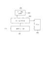
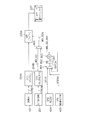
図2を参照して、本実施形態におけるSFB制御方式について説明する。本実施形態におけるデータのストア処理では、命令制御部201からストア要求(ストア命令)が送られると、それに対応して演算部202から送られるストア対象のデータが、1次キャッシュ制御部203内のストアバッファ部204及びライトバッファ部205を介して1次データキャッシュメモリ207にストアされる。本実施形態において、演算部202から送られたストア対象のデータは、ストアバッファ部204が有する複数のエントリのいずれかに格納された後に、ライトバッファ部205が有する複数のエントリのいずれかに格納され、その後1次データキャッシュメモリ207に格納される。
With reference to FIG. 2, the SFB control method in the present embodiment will be described. In the data store process according to the present embodiment, when a store request (store instruction) is sent from the
また、本実施形態におけるデータのロード処理では、命令制御部201からロード要求(ロード命令)が送られると、1次キャッシュ制御部203は、要求で指定されたストアポート番号のストアバッファのエントリ又はライトバッファのエントリに格納されているデータが、SFB候補のデータ(ロード対象のデータ)であるか否かを判定する。SFB候補のデータであるか否かの基本的な判定条件としては、(1)ストアする記憶領域の範囲内にロードしたい記憶領域が包含されている、(2)ストア対象のデータが既にレジスタにセットされている(データ受信済)、(3)ストア要求が例外などを起こさずに終了できる、がある。例えば、1次キャッシュ制御部203は、指定されたストアバッファのエントリ又はライトバッファのエントリに格納されている仮想アドレス(論理アドレス)VAやデータ長情報QBM等をチェックして、格納されているデータが、ロード対象のデータと同一の記憶領域にストアを行うストア処理待ちのデータであり、かつデータ長に係る条件を満足するか否かを判定する。SFB候補のデータであると1次キャッシュ制御部203が判定した場合、指定されたストアバッファのエントリ又はライトバッファのエントリに格納されているデータが演算部202に送られる。
Further, in the data loading process in the present embodiment, when a load request (load instruction) is sent from the
また、この判定処理と並行して、1次キャッシュ制御部203は、ストアバッファ部204が有する複数のエントリ及びライトバッファ部205が有する複数のエントリを検索し、それぞれに格納されているデータがSFB候補のデータとなり得るか否かを判定する。具体的には、1次キャッシュ制御部203のSFB候補選択処理部206が、ロード要求に係るアドレスやデータ長情報等を参照し、エントリ毎に、仮想アドレス(論理アドレス)VAやデータ長情報QBM等をチェックしてSFB候補のデータとなり得るか否かを判定する。さらに、SFB候補選択処理部206は、SFB候補のデータとなり得るものが複数ある場合、そのうちからロード命令に対して直近の(プログラム順で最も近い)ストア命令に係る1つのデータを選択して、SFB候補のデータとする。そして、決定したSFB候補のデータが格納されているストアバッファのエントリ又はライトバッファのエントリを指定するストアポート番号を持つ要求を発行させる。
In parallel with this determination processing, the primary
なお、要求で指定されたストアポート番号のストアバッファのエントリ又はライトバッファのエントリに格納されているデータがSFB候補のデータではなく、SFB候補のデータとなり得るデータを格納しているストアバッファのエントリ及びライトバッファのエントリもないと1次キャッシュ制御部203が判定した場合、1次キャッシュ制御部203は、1次データキャッシュメモリ207に対するデータのロード処理を実行する。
Note that the data stored in the store buffer entry or write buffer entry of the store port number specified in the request is not the SFB candidate data, but the store buffer entry storing the data that can be the SFB candidate data. When the primary
図3は、本実施形態における命令制御部201の構成例を示すブロック図である。なお、図3においては、メモリアクセス命令の実行に係る構成を示しているが、本実施形態における命令制御部201は、例えば演算命令や分岐命令等の他の命令の実行に係る構成も有している。
FIG. 3 is a block diagram illustrating a configuration example of the
図3において、命令制御部201は、命令デコード部301、リザベーションステーション(RSA)302、ポート割り当て部303、及びポート番号保持部304を有する。命令デコード部301は、供給される命令をデコードし、デコードした命令をそれぞれの機能の実行に対応したリザベーションステーションに格納する。デコードした命令が、例えばメモリアクセス命令(ロード命令、ストア命令)である場合、オペランドアドレス生成用のリザベーションステーション(RSA)302に格納され、例えば演算命令である場合、図示しない演算用のリザベーションステーション(RSE/RSF)に格納される。リザベーションステーション(RSA)302は、格納されたメモリアクセス命令が実行可能な状態になると1次キャッシュ部に対して該メモリアクセス命令を発行する。
In FIG. 3, the
ポート割り当て部303は、命令デコード部301でデコードしたメモリアクセス命令に対するポートの割り当てを行う。ポート割り当て部303は、命令デコード部301でデコードした命令がロード命令である場合、1次キャッシュ部で制御を行うフェッチポート(FP)のエントリ番号を割り当てる制御を行う。また、ポート割り当て部303は、命令デコード部301でデコードした命令がストア命令である場合、フェッチポート(FP)及びストア対象のデータを格納するためのストアポート(SP)のエントリ番号をそれぞれ割り当てる制御を行う。ここで、ストアポート(SP)のエントリ番号は、フェッチポート(FP)にも登録される。
The
ポート番号保持部304は、命令デコード部301でデコードした命令における最後のストア命令(直近のストア命令)に割り当てたストアポート(SP)のエントリ番号を保持する。ポート番号保持部304が保持するストアポート(SP)のエントリ番号は、命令デコード部301でデコードした命令がストア命令であるとき、そのストア命令に割り当てられたストアポート(SP)のエントリ番号に更新される。ポート番号保持部304が保持しているストアポート(SP)のエントリ番号は、命令制御部201が発行するロード命令に付加される。
The port
すなわち、本実施形態では、リザベーションステーション(RSA)302は、ストア命令を発行する際にポート割り当て部303により割り当てられたフェッチポート(FP)及びストアポート(SP)のエントリ番号を通知する。また、リザベーションステーション(RSA)302は、ロード命令を発行する際にポート割り当て部303により割り当てられたフェッチポート(FP)のエントリ番号に加え、ポート番号保持部304が保持しているストアポート(SP)のエントリ番号を通知する。このように本実施形態では、命令制御部201がロード命令を発行する際には、直近のストア命令に割り当てられたストアポート(SP)のエントリ番号を付加して発行する。
That is, in the present embodiment, the reservation station (RSA) 302 notifies the entry numbers of the fetch port (FP) and the store port (SP) allocated by the
なお、複数の命令を同時にデコードする場合において、ストア命令の後続の命令がロード命令であれば、そのロード命令には、ポート番号保持部304が保持しているストアポート(SP)のエントリ番号ではなく、同時にデコードしたストア命令に割り当てられたストアポート(SP)のエントリ番号を割り当てることで、直近のストア命令のストアポート(SP)のエントリ番号を持たせることが可能である。
When a plurality of instructions are decoded simultaneously, if the instruction subsequent to the store instruction is a load instruction, the load instruction includes the entry number of the store port (SP) held by the port
図4は、本実施形態におけるSFB制御に係る構成例を示す図である。セレクタ401は、パイプラインに投入される要求が命令制御部201からの要求REQであるか否かに応じた選択処理を行い、ストアポート番号SPID、選択制御信号SELA、SFBリターン信号SFBRを出力する。選択制御信号SELAは、選択対象がライトバッファであるかストアバッファであるかを示す信号であり、本実施形態では信号SELAが“1”である場合、ライトバッファを選択対象とし、信号SELAが“0”である場合、ストアバッファを選択対象とする。また、SFBリターン信号SFBRは、SFB制御に係るロード処理であるか否かを示す信号であり、本実施形態では信号SFBRが“1”である場合、SFB制御に係るロード処理であるとし、信号SFBRが“0”である場合、SFB制御に係るロード処理でないとする。
FIG. 4 is a diagram illustrating a configuration example related to SFB control in the present embodiment. The
パイプラインに投入される要求が命令制御部201からの要求REQである場合、セレクタ401は、命令制御部201から送付されるストアポート番号IU_SPIDをストアポート番号として出力し、選択制御信号SELAを“0”にし、SFBリターン信号SFBRを“1”にする。一方、パイプラインに投入される要求が命令制御部201からの要求REQでない場合、セレクタ401は、フェッチポート407から読み出したストアポート番号SU_SPID、選択制御信号SU_WBSEL、及びSFBリターン信号SU_SFBRを、ストアポート番号SPID、選択制御信号SELA、及びSFBリターン信号SFBRとしてそれぞれ出力する。
When the request input to the pipeline is the request REQ from the
セレクタ402は、ストアポート番号SPIDに対応するストアバッファ204Bのエントリ又はライトバッファ205Bのエントリから読み出した仮想アドレス(論理アドレス)VA、データ長情報QBM、及びフラグ情報FLG等を、選択制御信号SELAに応じて選択し出力する。選択制御信号SELAが“1”、すなわち選択対象がライトバッファである場合、セレクタ402は、ライトバッファ205Bから読み出した仮想アドレスVA、データ長情報QBM、及びフラグ情報FLG等を選択して出力する。また、選択制御信号SELAが“0”、すなわち選択対象がストアバッファである場合、セレクタ402は、ストアバッファ204Bから読み出した仮想アドレスVA、データ長情報QBM、及びフラグ情報FLG等を選択して出力する。
The
セレクタ403は、パイプラインに投入される要求が命令制御部201からの要求REQであるか否かに応じて、アドレス生成部(EAG)又はレジスタの出力SU_ADを選択し出力する。パイプラインに投入される要求が命令制御部201からの要求REQである場合、セレクタ403は、アドレス生成部(EAG)から出力される仮想アドレスVA及びデータ長情報QBMを選択して出力する。また、パイプラインに投入される要求が命令制御部201からの要求REQでない場合、セレクタ403は、レジスタから出力される仮想アドレスVA及びデータ長情報QBMを選択して出力する。レジスタには、パイプラインに命令制御部201からの要求REQが投入されるときにアドレス生成部(EAG)によって生成された仮想アドレスVA及びデータ長情報QBMが保持されている。
The
SFB判定部404は、セレクタ401からのSFBリターン信号SU_SFBR、セレクタ402の出力、及びセレクタ403の出力に基づいて、SFB制御によるストアバッファ204Aのエントリ又はライトバッファ205Bのエントリからのデータのロードが可能であるか否かを判定し、判定結果に応じた選択制御信号SELBを出力する。SFB判定部404は、SFBリターン信号SU_SFBRが“1”、すなわちSFB制御に係るロード処理であることを示し、セレクタ402から出力された仮想アドレスVA、データ長情報QBM、及びフラグ情報FLG等、及びセレクタ403から出力された仮想アドレスVA及びデータ長情報QBMを基に有効なSFB候補のデータがあると判断した場合、SFB制御によるデータのロードが可能であると判定する。
Based on the SFB return signal SU_SFBR from the
SFB候補判定部405は、ストアバッファのエントリ及びライトバッファのエントリを検索し、それぞれに格納されているデータがSFB候補のデータとなり得るか否かを判定する。具体的には、SFB候補判定部405は、セレクタ403から出力された仮想アドレスVA及びデータ長情報QBMを参照し、エントリ毎に仮想アドレスVAやデータ長情報QBM等をチェックしてSFB候補のデータとなり得るか否かを判定する。また、SFB候補判定部405は、SFB候補のデータとなり得るデータがあった場合、SFBサーチヒット信号SFBSHを出力するとともに、SFB候補のデータとなり得るデータが格納されたストアバッファのエントリ及びライトバッファのエントリに対応するストアポート番号を出力する。
The SFB
SFB候補決定部406は、SFB候補判定部405によりSFB候補のデータとなり得ると判定されたデータのいずれか1つのデータをSFB候補のデータとして選択する。SFB候補決定部406は、SFB候補判定部405から出力されたSFB候補のデータとなり得るデータが格納されたストアバッファのエントリ及びライトバッファのエントリに対応するストアポート番号のうちからプログラム順で最も近い位置にあるストア命令に対して割り当てられたストアポート番号を選択してSFB候補のストアポート番号SFB_SPIDとして出力する。また、SFB候補決定部406は、選択したストアポート番号がストアバッファ又はライトバッファのどちらのストアポート番号かを示す信号WBSELを出力する。
The SFB
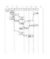
図9に示す例を参照して、SFB候補決定部406によるSFB候補の決定方法について説明する。図9には、ストアバッファが24個のエントリを有し、ライトバッファが6個のエントリを有する例を示している。直近のストア命令にストアポート番号15のストアバッファのエントリが割り当てられ、そのストア命令の後に、ロード要求が発行されたとする。
With reference to the example illustrated in FIG. 9, the SFB candidate determination method by the SFB
このロード要求と同一の記憶領域にデータをストアするストア命令に対して、ストアポート番号7、3のストアバッファのエントリ、ストアポート番号2のライトバッファのエントリが割り当てられているものとする。このうち、ストアポート番号3のストアバッファのエントリに格納されたデータは、ロード命令でロードするデータ長よりもデータ長が短いため、SFB候補とはならずにSFI候補となる。ここで、SFI(Store-Fetch-Interlock、ストアフェッチインターロック)とは、フェッチしたいが同一アクセス領域にフェッチを阻害するストアがある状態である。
Assume that a store buffer entry with
したがって、ストアポート番号7のストアバッファのエントリ、及びストアポート番号2のライトバッファのエントリにそれぞれ格納されたデータがSFB候補となりうる。このとき、SFB候補決定部406は、直近のストア命令に割り当てられたストアポート番号からストアバッファのトップオブキュー(STB−TOQ)に向かい、続いてライトバッファのボトムオブキュー(WB−BOQ)からライトバッファのトップオブキュー(WB−TOQ)に向かう方向において、最も近いSFB候補(図9に示す例では、ストアポート番号7のストアバッファのエントリ)をSFB候補のデータとして決定する。
Accordingly, the data stored in the store buffer entry of
フェッチポート(FP)407は、命令制御部201からのロード要求やストア要求を保持するポートである。SFBサーチヒット信号SFBSHが出力されると、フェッチポート(FP)407にSFBリターンフラグがセットされ、信号WBSELが出力されると、フェッチポート(FP)407にSFB候補のデータがストアバッファのエントリにあるかライトバッファのエントリにあるかを示すフラグがセットされる。また、SFB候補決定部406から出力されたSFB候補のストアポート番号SFB_SPIDが、フェッチポート(FP)407にセットされる。フェッチポート(FP)407にセットされるSFBリターンフラグ、SFB候補のデータがストアバッファのエントリにあるかライトバッファのエントリにあるかを示すフラグ、及びSFB候補のストアポート番号は、それぞれSFBリターン信号SU_SFBR、選択制御信号SU_WBSEL、及びストアポート番号SU_SPIDとして読み出される。
A fetch port (FP) 407 is a port that holds a load request and a store request from the
セレクタ408は、ストアポート番号SPIDに対応するストアバッファ204Aのエントリ又はライトバッファ205Aのエントリからロードしたデータを、選択制御信号SELAに応じて選択しSFBデータSFBDとして出力する。選択制御信号SELAが“1”、すなわち選択対象がライトバッファである場合、セレクタ408は、ライトバッファ205AのエントリからロードしたデータをSFBデータSFBDとして出力する。また、選択制御信号SELAが“0”、すなわち選択対象がストアバッファである場合、セレクタ408は、ストアバッファ204Aのエントリからロード読み出したデータをSFBデータSFBDとして出力する。
The
セレクタ410は、ストアバッファ204A又はライトバッファ205AからロードしたSFBデータSFBD、又は1次データキャッシュメモリ207からロードしウェイ選択部409を介して出力されたデータRAMDを、選択制御信号SELBに応じて選択し演算部202に出力する。選択制御信号SELBがSFB制御によるデータのロードが可能であることを示す場合、セレクタ410は、ストアバッファ204A又はライトバッファ205AからのSFBデータSFBDを選択して演算部202に出力する。また、選択制御信号SELBがSFB制御によるデータのロードが可能であることを示さない場合、セレクタ410は、1次データキャッシュメモリ207からのデータRAMDを選択して演算部202に出力する。
The
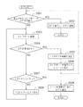
次に、本実施形態におけるロード命令の処理動作について説明する。図5は、本実施形態におけるロード命令の処理例を示すフローチャートである。命令制御部201からロード要求(ロード)命令が発行されると、ステップS501にて、ロード要求を受けた1次キャッシュ制御部203は、要求において指定されたストアポートがSFB可能であるか否かを判定する。すなわち、1次キャッシュ制御部203は、要求において指定されたストアポート番号のストアバッファのエントリ又はライトバッファのエントリに格納されているデータがSFB候補のデータであるか否かを判定する。
Next, a load instruction processing operation in this embodiment will be described. FIG. 5 is a flowchart showing a processing example of a load instruction in the present embodiment. When a load request (load) instruction is issued from the
1次キャッシュ制御部203が、指定されたストアポートがSFB可能である、すなわち指定されたストアポート番号のストアバッファのエントリ又はライトバッファのエントリに格納されているデータがSFB候補のデータであると判定した場合(S501のYES)、ステップS502にて、1次キャッシュ制御部203は、SFB制御によるデータのロードを実行する。具体的には、1次キャッシュ制御部203は、指定されたストアポート番号のストアバッファのエントリ又はライトバッファのエントリからデータをロードして演算部202に送る。そして、1次キャッシュ制御部203は、ロード要求が正常に完了したことを示す信号STV(STatus Valid)を命令制御部201に返して処理を終了する。
The primary
1次キャッシュ制御部203が、指定されたストアポートがSFB可能ではないと判定した場合(S501のNO)、ステップS503にて、1次キャッシュ制御部203は、ストアバッファが有する複数のエントリ及びライトバッファが有する複数のエントリを検索し、それぞれに格納されているデータがSFB候補のデータとなり得るか否かを判定する。続いて、ステップS504にて、1次キャッシュ制御部203は、ストアバッファ及びライトバッファにSFB候補のデータとなり得るデータがあったか否かを判定する。
If the primary
SFB候補のデータとなり得るデータがストアバッファ及びライトバッファにあったと1次キャッシュ制御部203が判定した場合(S504のYES)、ステップS505にて、1次キャッシュ制御部203は、SFB候補のデータとなり得るデータのうちから直近のストア命令による1つのデータをSFB候補のデータに決定する。次に、ステップS506にて、1次キャッシュ制御部203は、決定したSFB候補のデータが格納されているストアバッファのエントリ又はライトバッファのエントリに対応するストアポート番号を指定してロード要求を発行させ、ステップS501に戻る。
When the primary
ステップS506から戻ったステップS501では、1次キャッシュ制御部203が、命令制御部201からロード要求を受けたときと同様に、要求において指定されたストアポートがSFB可能であるか否かを判定する。このとき、指定されたストアポート番号のストアバッファのエントリ及びライトバッファのエントリに格納されているデータはSFB候補のデータとなり得ると判定されているデータである。したがって、ステップS502に進み、1次キャッシュ制御部203は、SFBによるデータのロードを実行してデータを演算部202に送り、信号STVを命令制御部201に返して処理を終了する。
In step S501 that has returned from step S506, the primary
ステップS504において、SFB候補のデータとなり得るデータがストアバッファ及びライトバッファにないと1次キャッシュ制御部203が判定した場合(NO)、ステップS507にて、1次キャッシュ制御部203は、1次データキャッシュメモリ207にロード対象のデータが格納されているか否かを判定する。1次データキャッシュメモリ207にロード対象のデータが格納されていると1次キャッシュ制御部203が判定した場合、すなわち1次キャッシュヒットと判定した場合(S507のYES)、ステップS508にて、1次キャッシュ制御部203は、1次データキャッシュメモリ207からデータをロードして演算部202に送る。そして、1次キャッシュ制御部203は、ロード要求が正常に完了したことを示す信号STVを命令制御部201に返して処理を終了する。
In step S504, when the primary
一方、1次データキャッシュメモリ207にロード対象のデータがないと1次キャッシュ制御部203が判定した場合、すなわち1次キャッシュミスと判定した場合(S507のNO)、ステップS509にて、1次キャッシュ制御部203は、下位側(例えば2次キャッシュメモリ)にロード要求を発行してステップS503に戻る。なお、1次キャッシュ制御部203が下位側にロード要求を発行してからステップS503に戻るのは、下位側に対するロード要求においてはデータのロード処理に時間がかかるため、その間にストアバッファのエントリ及びライトバッファのエントリにSFB候補のデータとなり得るデータが格納された場合に速やかに検出しSFB制御によるデータのロードを行うためである。
On the other hand, when the primary
なお、図5に示したフローチャートでは、説明をわかり易くするために、要求において指定されたストアポートに格納されているデータがSFB候補のデータであるか否かを判定する動作を行った後に、ストアポートの検索を行ってSFB候補のデータを決定する動作を行うようにしているが、指定されたストアポートに格納されているデータがSFB候補のデータであるか否かを判定する動作とストアポートの検索を行ってSFB候補のデータを決定する動作とは並行して実行する。 In the flowchart shown in FIG. 5, for the sake of easy understanding, after the operation of determining whether the data stored in the store port specified in the request is the SFB candidate data, The operation of determining the SFB candidate data by performing the port search is performed. The operation and the store port for determining whether or not the data stored in the designated store port is the SFB candidate data. This is performed in parallel with the operation of performing the above search to determine the data of the SFB candidate.
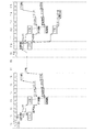
図6は、本実施形態におけるSFB制御によるロード処理の例を示すタイムチャートである。図6には、命令制御部201(外部)からのロード要求で指定されたストアポート番号のストアバッファのエントリ又はライトバッファのエントリのデータがSFB候補のデータではなく、ストアバッファのエントリ及びライトバッファのエントリを検索してSFB候補のデータを決定し、データのロードを行う例を示している。SFB候補のデータは、ストアポート番号がSP#Aであるストアバッファのエントリ又はライトバッファのエントリに格納されているものとする。 FIG. 6 is a time chart showing an example of load processing by SFB control in the present embodiment. In FIG. 6, the store buffer entry or write buffer entry data of the store port number designated by the load request from the instruction control unit 201 (external) is not SFB candidate data, but store buffer entries and write buffers. In this example, the SFB candidate data is determined by searching the entries, and the data is loaded. It is assumed that the SFB candidate data is stored in the store buffer entry or the write buffer entry whose store port number is SP # A.
時刻T1において、命令制御部201から、SP#Aと異なるストアポート番号が指定されたロード要求が入力され、1次キャッシュ制御部203のパイプラインに投入される。このとき、命令制御部201からのロード要求で指定されたストアポート番号に基づいてストアバッファ及びライトバッファへのアクセスが行われる。時刻T2において、アドレス生成部によって生成されたアドレス等の選択が行われ、ストアバッファ及びライトバッファからの信号読み出しが行われる。
At time T1, a load request in which a store port number different from SP # A is specified is input from the
そして、命令制御部201からのロード要求で指定されたストアポート番号に従ってストアバッファ及びライトバッファから読み出した信号と、アドレス生成部によって生成されたアドレス等に基づいて、SFB制御によるデータのロードが可能であるか判定が行われ(時刻T3)、SFB制御によるデータのロードが可能ではないと判定すると、パイプラインをアボートする(時刻T5)。このとき、命令制御部201に対するSTV通知は行われない。
Then, based on the signal read from the store buffer and the write buffer according to the store port number specified by the load request from the
また、アドレス生成部によって生成されたアドレス等を参照してストアバッファのエントリ及びライトバッファのエントリが検索され、格納されているデータがSFB候補のデータとなり得るかの判定が行われ(時刻T3)、1つのSFB候補のデータが選択される(時刻T4)。この例では、ストアポート番号がSP#Aであるストアバッファのエントリ又はライトバッファのエントリに格納されているデータがSFB候補のデータとして選択される。 Further, the store buffer entry and the write buffer entry are searched with reference to the address generated by the address generator, and a determination is made as to whether the stored data can be SFB candidate data (time T3). One SFB candidate data is selected (time T4). In this example, data stored in the store buffer entry or the write buffer entry whose store port number is SP # A is selected as the SFB candidate data.
その後、時刻T10において、ストアポート番号としてSP#Aが指定されたロード要求(内部リクエスト)が1次キャッシュ制御部203のパイプラインに投入される。そしてロード要求で指定されたストアポート番号SP#Aに基づいてストアバッファ及びライトバッファへのアクセスが行われる。時刻T11において、ストアバッファ及びライトバッファからの信号読み出しが行われる。
Thereafter, at time T <b> 10, a load request (internal request) in which SP # A is specified as the store port number is input to the pipeline of the primary
そして、ロード要求で指定されたストアポート番号SP#Aに従ってストアバッファ及びライトバッファから読み出した信号と、アドレス生成部によって生成されたアドレス等に基づいて、SFB制御によるデータのロードが可能であるか判定が行われる(時刻T12)。判定の結果、SFB制御によるデータのロードが可能であると判定すると(時刻T13)、時刻T13においてストアポート番号SP#Aのストアバッファのエントリ又はライトバッファのエントリからロードしたデータ(SFBデータ)を演算部202へ出力する(時刻T14)そして、時刻T15において、命令制御部201に対するSTV通知が行われ、データのロード処理が終了する。
Whether data can be loaded by SFB control based on the signal read from the store buffer and write buffer according to the store port number SP # A specified in the load request, the address generated by the address generation unit, and the like. A determination is made (time T12). As a result of the determination, if it is determined that data can be loaded by SFB control (time T13), the data loaded from the store buffer entry or the write buffer entry of the store port number SP # A at time T13 (SFB data) is obtained. The data is output to the arithmetic unit 202 (time T14). At time T15, an STV notification is sent to the
なお、時刻T12以降においても、生成されているアドレス等を参照してのストアバッファのエントリ及びライトバッファのエントリの検索、及びSFB候補のデータとなり得るかの判定、及び1つのSFB候補のデータの選択が行われる。しかし、時刻T12以降におけるこれらの処理結果は、時刻T15において、命令制御部201に対するSTV通知が行われ、データのロード処理が終了されるので、捨てられることとなり動作に影響を及ぼすことはない。
Even after time T12, the search of the store buffer entry and the write buffer entry with reference to the generated address and the like, the determination of whether the data can be SFB candidate, and the data of one SFB candidate data A selection is made. However, these processing results after time T12 are discarded because the STV notification is sent to the
図7は、本実施形態におけるSFB制御によるロード処理の他の例を示すタイムチャートである。図7には、命令制御部201(外部)からのロード要求で指定されたストアポート番号のストアバッファのエントリ又はライトバッファのエントリのデータがSFB候補のデータである例を示している。SFB候補のデータは、ストアポート番号がSP#Aであるストアバッファのエントリ又はライトバッファのエントリに格納されているものとする。 FIG. 7 is a time chart showing another example of load processing by SFB control in the present embodiment. FIG. 7 shows an example in which the data of the store buffer entry or the write buffer entry of the store port number specified by the load request from the instruction control unit 201 (external) is SFB candidate data. It is assumed that the SFB candidate data is stored in the store buffer entry or the write buffer entry whose store port number is SP # A.
時刻T1において、命令制御部201から、ストアポート番号としてSP#Aが指定されたロード要求が入力され、1次キャッシュ制御部203のパイプラインに投入される。このとき、命令制御部201からのロード要求で指定されたストアポート番号に基づいてストアバッファ及びライトバッファへのアクセスが行われる。時刻T2において、アドレス生成部によって生成されたアドレス等の選択が行われ、ストアバッファ及びライトバッファからの信号読み出しが行われる。
At time T <b> 1, a load request in which SP # A is specified as the store port number is input from the
そして、ロード要求で指定されたストアポート番号SP#Aに従ってストアバッファ及びライトバッファから読み出した信号と、アドレス生成部によって生成されたアドレス等に基づいて、SFB制御によるデータのロードが可能であるか判定が行われる(時刻T3)。判定の結果、SFB制御によるデータのロードが可能であると判定すると(時刻T4)、判定と並行して時刻T3においてストアポート番号SP#Aのストアバッファのエントリ又はライトバッファのエントリからロードしたデータ(SFBデータ)を演算部202へ出力する(時刻T5)そして、時刻T6において、命令制御部201に対するSTV通知が行われ、データのロード処理が終了する。
Whether data can be loaded by SFB control based on the signal read from the store buffer and write buffer according to the store port number SP # A specified in the load request, the address generated by the address generation unit, and the like. A determination is made (time T3). As a result of the determination, if it is determined that data can be loaded by SFB control (time T4), the data loaded from the store buffer entry of the store port number SP # A or the write buffer entry at time T3 in parallel with the determination. (SFB data) is output to the arithmetic unit 202 (time T5). At time T6, an STV notification is sent to the
この図7に示す例においても、アドレス生成部によって生成されたアドレス等を参照してのストアバッファのエントリ及びライトバッファのエントリの検索、及びSFB候補のデータとなり得るかの判定、及び1つのSFB候補のデータの選択が行われる。しかし、これらの処理結果は、時刻T6において、命令制御部201に対するSTV通知が行われ、データのロード処理が終了されるので、捨てられることとなり動作に影響を及ぼすことはない。
Also in the example shown in FIG. 7, the search of the store buffer entry and the write buffer entry with reference to the address generated by the address generation unit, the determination of whether or not the data can be SFB candidate, and one SFB Candidate data is selected. However, since these processing results are notified of STV to the
ここで、SFB候補のデータの検索を行ってからSFB候補のデータを読み出すまでには一定の時間経過を伴うため、新規にSFB候補のデータとなるストア命令がストアバッファに設定される場合がある。この新規に設定されるストア命令が直近のストア命令である場合、SFB候補のデータのロード処理をアボートし、SFB候補のデータをロードするためのストアポート番号を更新した後にSFB候補のデータのロード処理を行えばよい。例えば、図9に示した例では、ストアポート番号7のストアバッファのエントリのデータをSFB候補のデータに決定してから、SFB候補であるストアポート番号7と直近のストア命令に割り当てられたストアポート番号15との間のストアバッファのエントリに新規にSFB候補のデータとなるストア命令が設定されていないかをチェックするようにすればよい。
Here, since a certain amount of time elapses after the search for the SFB candidate data until the SFB candidate data is read out, a store instruction that newly becomes the SFB candidate data may be set in the store buffer. . When the newly set store instruction is the latest store instruction, the loading process of the SFB candidate data is aborted, and after the store port number for loading the SFB candidate data is updated, the SFB candidate data is loaded. What is necessary is just to process. For example, in the example shown in FIG. 9, after the data of the
本実施形態によれば、命令制御部201からロード命令が発行されると、1次キャッシュ制御部203は、ストアバッファのエントリ及びライトバッファのエントリを検索して、格納されているデータがSFB候補のデータとなり得るか否かを判定する。そして、SFB候補のデータとなり得るデータが複数存在する場合には、1次キャッシュ制御部203は、そのうちからロード命令に対して直近のストア命令に係る1つのデータをSFB候補のデータに決定して、SFB制御によるデータのロードを行う。これにより、SFB候補のデータになり得るデータがストアバッファ及びライトバッファに複数存在しても、それらのストア処理を待たずに1つのデータを適切に選択してSFB制御によるデータのロードを実行することができ、プロセッサの処理性能を向上させることができる。
According to the present embodiment, when a load instruction is issued from the
また、ロード命令によりロードするデータが直近のストア命令でストアするデータである場合が多いので、命令制御部201からロード命令を発行する際、直近のストア命令に対して割り当てられたストアポートのエントリ番号をロード命令とともに通知することで、SFB候補のデータとなり得るデータの検索を待たずに、SFB制御によるデータのロードを行うことが可能となり、プロセッサの処理性能を向上させることができる。
Further, since the data loaded by the load instruction is often the data stored by the latest store instruction, when issuing the load instruction from the
本実施形態のようにストアバッファとライトバッファとを有する構成においてのデータのストア処理は、次のように行われる。まず、命令制御部201から発行されたストア命令は、1次キャッシュ制御部203でストアバッファに一旦格納される。並行して、演算部202から1次キャッシュ制御部203にストア対象のデータも送付される。アドレス例外等の例外要因がなく正常にストア処理できる状態であれば、1次キャッシュ制御部203は、命令制御部に信号STVを返す。これを受けて命令制御部201は、ストア命令を完了(コミットさせる)。つまり、1次データキャッシュメモリ207に実際にストア対象のデータがストアされる前にストア命令がコミットされる(ストア命令の突き離し制御)ことにより、ストア命令を高速処理している。命令制御部201から1次キャッシュ制御部203にストア命令のコミット通知が送付されると、1次キャッシュ制御部203は、ストア対象のデータをストアバッファからライトバッファに移動する(移動を指示する信号をライトバッファゴー信号WB_GOと称する)。その後、ライトバッファから1次キャッシュ制御部203のパイプラインを起動して、実際に1次データキャッシュメモリ207へのストア動作を行う。
Data storage processing in a configuration having a store buffer and a write buffer as in the present embodiment is performed as follows. First, the store instruction issued from the
このようなストア動作において、本実施形態におけるSFB制御方式では、ストアバッファのエントリに格納されているデータをSFB候補のデータと決定した後、データのロードを行う前にSFB候補のデータがストアバッファからライトバッファに移動してしまうことが考えられる。この場合、SFB候補のデータがストアバッファに存在しないため、データをロードするためのパイプラインがアボートしてしまい、処理時間が増大してしまう。そこで、図8に示すような制御機構を設け、SFB候補のデータを決定した後にストアバッファからライトバッファにSFB候補のデータが移動することを数サイクル間抑止する。 In such a store operation, in the SFB control method according to the present embodiment, after the data stored in the entry of the store buffer is determined as the SFB candidate data, the SFB candidate data is stored in the store buffer before the data is loaded. It is possible to move from to the write buffer. In this case, since the SFB candidate data does not exist in the store buffer, the pipeline for loading the data is aborted, and the processing time increases. Therefore, a control mechanism as shown in FIG. 8 is provided to suppress the movement of the SFB candidate data from the store buffer to the write buffer for several cycles after the SFB candidate data is determined.
図8は、本実施形態におけるストアバッファからライトバッファへのストア制御に係る構成例を示す図である。命令制御部201からストア命令のコミット通知STRCMがストアバッファ204Bに送付されると、ストアバッファ204Bは、第1のライトバッファゴー信号WB_GOを出力する。また、ストア命令に係る演算部202から出力されるストア対象のデータSTRDTは、ストアバッファ204A、及びライトバッファ205Aを介して1次データキャッシュメモリ207にストアされる。このとき、ストアバッファ204Aからライトバッファ205Aへのストア対象のデータのストアは、第2のライトバッファゴー信号WB_GOAに従って実行される。
FIG. 8 is a diagram showing a configuration example relating to store control from the store buffer to the write buffer in the present embodiment. When a store instruction commit notification STRCM is sent from the
AND(論理積演算)回路801は、SFB判定部404から出力される選択制御信号SELB、SFB候補判定部405から出力されるSFBサーチヒット信号SFBSH、及びライトバッファゴー抑止信号WB_GO_INHが入力され、演算結果をカウンタ制御信号CNTENとして出力する。具体的には、AND回路801は、選択制御信号SELBが“0”、SFBサーチヒット信号SFBSHが“1”、ライトバッファゴー抑止信号WB_GO_INHが“0”である場合、カウンタ制御信号CNTENを“1”にし、それ以外はカウンタ制御信号CNTENを“0”にする。すなわち、カウンタ制御信号CNTENが“0”である状態で、SFB制御によるデータのロードが可能ではなく、ストアバッファのエントリ及びライトバッファのエントリを検索してSFB候補のデータとなり得るデータが見つかった場合、カウンタ制御信号CNTENが“1”となる。
An AND (logical product operation)
カウンタ802は、カウンタ制御信号CNTENが“0”から“1”に変化したとき、カウント値を所定の値に設定し、1サイクル毎に1ずつデクリメントする。所定の値は、第1のライトバッファゴー信号WB_GOの伝達を抑止したい期間に応じて決めればよく、例えば8サイクルの期間抑止したい場合には“8”に設定すればよい。OR(論理和演算)回路803は、カウンタ802の出力が入力され、演算結果をライトバッファゴー抑止信号WB_GO_INHとして出力する。本実施形態では、OR回路803は、カウンタ802のカウント値が“0”でない(出力ビットの少なくとも1つが“1”である)場合、ライトバッファゴー抑止信号WB_GO_INHを“1”にし、カウンタ802のカウント値が“0”である(出力ビットのすべてが“0”である)場合、ライトバッファゴー抑止信号WB_GO_INHを“0”にする。
When the counter control signal CNTEN changes from “0” to “1”, the
AND回路804は、第1のライトバッファゴー信号WB_GO及びライトバッファゴー抑止信号WB_GO_INHが入力され、演算結果を第2のライトバッファゴー信号WB_GOAとして出力する。AND回路804は、ライトバッファゴー抑止信号WB_GO_INHが“1”である場合、第1のライトバッファゴー信号WB_GOにかかわらず、第2のライトバッファゴー信号WB_GOAを“0”(ライトバッファへのストア対象のデータのストア不許可)にし、第1のライトバッファゴー信号WB_GOが伝達されることを抑止する。また、AND回路804は、ライトバッファゴー抑止信号WB_GO_INHが“0”である場合、第1のライトバッファゴー信号WB_GOを第2のライトバッファゴー信号WB_GOAとして出力する。したがって、ライトバッファゴー抑止信号WB_GO_INHが“0”である場合、第1のライトバッファゴー信号WB_GOが“0”であれば第2のライトバッファゴー信号WB_GOAを“0”(ライトバッファへのストア対象のデータのストア不許可)にし、第1のライトバッファゴー信号WB_GOが“1”であれば第2のライトバッファゴー信号WB_GOAを“1”(ライトバッファへのストア対象のデータのストア許可)にする。
The AND
図8に示した構成によれば、ストアバッファのエントリに格納されているデータをSFB候補のデータと決定した後、所定の期間においてSFB候補のデータがライトバッファに移動するのを抑止することができ、処理時間を増大させることなく、SFB制御によるデータのロードを行うことが可能になる。なお、カウンタ802のカウント値が次々に所定の値に設定されてストアバッファからライトバッファへのデータの移動が滞ることを防止するために、カウンタ802のカウント値が“0”になった後、カウンタ制御信号CNTENが“1”になることを抑止することが好ましい。すなわち、ストアバッファからライトバッファへのストアの抑止を解除してから所定の期間は、ストアバッファからライトバッファへのストアの抑止を禁止する(ストア処理許可状態にし続ける)ことが好ましい。
According to the configuration shown in FIG. 8, after the data stored in the entry of the store buffer is determined as the SFB candidate data, the SFB candidate data is prevented from moving to the write buffer in a predetermined period. Thus, it is possible to load data by SFB control without increasing the processing time. In addition, after the count value of the
なお、前記実施形態は、何れも本発明を実施するにあたっての具体化のほんの一例を示したものに過ぎず、これらによって本発明の技術的範囲が限定的に解釈されてはならないものである。すなわち、本発明はその技術思想、またはその主要な特徴から逸脱することなく、様々な形で実施することができる。 The above-described embodiments are merely examples of implementation in carrying out the present invention, and the technical scope of the present invention should not be construed as being limited thereto. That is, the present invention can be implemented in various forms without departing from the technical idea or the main features thereof.
110 プロセッサ
111、201 命令制御部
112、202 演算部
113 1次キャッシュ部
114、203 1次キャッシュ制御部
115 1次命令キャッシュメモリ
116、207 1次データキャッシュメモリ
117 2次キャッシュ部
120 主記憶装置
204 ストアバッファ部
205 ライトバッファ部
206 SFB候補選択処理部
301 命令デコード部
302 リザベーションステーション
303 ポート割り当て部
304 ポート番号保持部
404 SFB判定部
405 SFB候補判定部
406 SFB候補決定部
407 フェッチポート
110
Claims (8)
前記命令制御部から発行されるストア命令の対象であるストア対象データがストアされるキャッシュメモリと、
前記命令制御部と前記キャッシュメモリとの間で、前記ストア対象データを格納するエントリを複数有するバッファ部と、
前記命令制御部からロード命令が発行された場合、複数の前記エントリを検索して前記ロード命令の対象であるロード対象データが有るとき、前記ロード対象データのいずれか1つを選択する選択処理部と、
前記選択処理部が選択したロード対象データを前記バッファ部から読み出して出力する読み出し制御部とを有することを特徴とする演算処理装置。 An instruction control unit for issuing instructions;
A cache memory in which store target data that is a target of a store instruction issued from the instruction control unit is stored;
A buffer unit having a plurality of entries for storing the store target data between the instruction control unit and the cache memory;
When a load instruction is issued from the instruction control unit, when there is load target data that is a target of the load instruction by searching a plurality of the entries, a selection processing unit that selects any one of the load target data When,
An arithmetic processing apparatus comprising: a read control unit that reads out and outputs the load target data selected by the selection processing unit from the buffer unit.
前記エントリ毎に格納されているデータが前記ロード対象データであるか否かを判定する判定部と、
前記判定部が前記ロード対象データであると判定したデータのいずれか1つを選択する決定部とを有することを特徴とする請求項1記載の演算処理装置。 The selection processing unit
A determination unit that determines whether data stored for each entry is the load target data; and
The arithmetic processing apparatus according to claim 1, further comprising: a determination unit that selects any one of the data determined to be the load target data by the determination unit.
前記読み出し制御部は、前記エントリを示す情報によって指定される前記エントリに格納されているデータが前記ロード対象データである場合、該エントリからデータを読み出して出力することを特徴とする請求項1又は2記載の演算処理装置。 The instruction control unit, when issuing the load instruction, outputs information indicating the entry assigned to the store instruction immediately before the load instruction together with the load instruction,
The read control unit, when the data stored in the entry specified by the information indicating the entry is the data to be loaded, reads out the data from the entry and outputs the data. 2. The arithmetic processing apparatus according to 2.
前記エントリを示す情報を保持し、前記ストア命令に対して前記エントリを割り当てる制御を行う毎に保持する前記エントリを示す情報を更新する情報保持部を有し、
前記ロード命令を発行する際、前記情報保持部が保持している前記エントリを示す情報を前記ロード命令とともに出力することを特徴とする請求項3記載の演算処理装置。 The command control unit
An information holding unit that holds information indicating the entry and updates the information indicating the entry that is held every time control for assigning the entry to the store instruction is performed;
4. The arithmetic processing apparatus according to claim 3, wherein when the load instruction is issued, information indicating the entry held by the information holding unit is output together with the load instruction.
前記選択処理部が前記ロード対象データを選択してから、所定の期間は前記ストアバッファ部から前記ライトバッファ部へのデータの書き込みを抑止する書き込み制御部を有することを特徴とする請求項1〜4の何れか1項に記載の演算処理装置。 The buffer unit includes a store buffer unit having a plurality of entries for storing the store target data, and a write buffer unit having a plurality of entries for storing the store target data between the store buffer unit and the cache memory. ,
The write control unit for suppressing writing of data from the store buffer unit to the write buffer unit for a predetermined period after the selection processing unit selects the load target data. 5. The arithmetic processing apparatus according to any one of 4.
前記命令制御部からロード命令が発行された場合、複数の前記エントリを検索して前記ロード命令の対象であるロード対象データが有るとき、前記ロード対象データのいずれか1つを選択し、
前記選択したロード対象データを前記バッファ部から読み出して出力することを特徴とする演算処理装置の制御方法。 An instruction control unit that issues an instruction; a cache memory that stores data to be stored that is a target of a store instruction issued from the instruction control unit; and the store target between the instruction control unit and the cache memory. A control method for an arithmetic processing unit having a buffer unit having a plurality of entries for storing data,
When a load instruction is issued from the instruction control unit, when there is load target data that is a target of the load instruction by searching a plurality of the entries, any one of the load target data is selected,
A control method for an arithmetic processing unit, wherein the selected load target data is read from the buffer unit and output.
Priority Applications (2)
| Application Number | Priority Date | Filing Date | Title |
|---|---|---|---|
| JP2016082197A JP6680978B2 (en) | 2016-04-15 | 2016-04-15 | Arithmetic processing device and method for controlling arithmetic processing device |
| US15/415,941 US10146441B2 (en) | 2016-04-15 | 2017-01-26 | Arithmetic processing device and method for controlling arithmetic processing device |
Applications Claiming Priority (1)
| Application Number | Priority Date | Filing Date | Title |
|---|---|---|---|
| JP2016082197A JP6680978B2 (en) | 2016-04-15 | 2016-04-15 | Arithmetic processing device and method for controlling arithmetic processing device |
Publications (2)
| Publication Number | Publication Date |
|---|---|
| JP2017191561A true JP2017191561A (en) | 2017-10-19 |
| JP6680978B2 JP6680978B2 (en) | 2020-04-15 |
Family
ID=60038146
Family Applications (1)
| Application Number | Title | Priority Date | Filing Date |
|---|---|---|---|
| JP2016082197A Active JP6680978B2 (en) | 2016-04-15 | 2016-04-15 | Arithmetic processing device and method for controlling arithmetic processing device |
Country Status (2)
| Country | Link |
|---|---|
| US (1) | US10146441B2 (en) |
| JP (1) | JP6680978B2 (en) |
Families Citing this family (1)
| Publication number | Priority date | Publication date | Assignee | Title |
|---|---|---|---|---|
| CN108255417B (en) * | 2017-11-30 | 2020-11-24 | 平安科技(深圳)有限公司 | Data access method, electronic device and readable storage medium |
Citations (4)
| Publication number | Priority date | Publication date | Assignee | Title |
|---|---|---|---|---|
| JPH04107634A (en) * | 1990-08-28 | 1992-04-09 | Nec Corp | Memory data bypass control system |
| JP2004038341A (en) * | 2002-06-28 | 2004-02-05 | Fujitsu Ltd | Storage control device and data storage method |
| JP2007527563A (en) * | 2003-07-08 | 2007-09-27 | アドバンスト・マイクロ・ディバイシズ・インコーポレイテッド | Store-load forward (STL) buffer with indexed lookup |
| JP2015210577A (en) * | 2014-04-24 | 2015-11-24 | 富士通株式会社 | Arithmetic processing device and control method of arithmetic processing device |
Family Cites Families (16)
| Publication number | Priority date | Publication date | Assignee | Title |
|---|---|---|---|---|
| JPH0812646B2 (en) * | 1989-03-03 | 1996-02-07 | 三菱電機株式会社 | Semiconductor integrated circuit |
| JP3400824B2 (en) * | 1992-11-06 | 2003-04-28 | 三菱電機株式会社 | Semiconductor storage device |
| EP1211681B1 (en) * | 1998-01-20 | 2007-02-14 | Fujitsu Limited | Data storage device and control method therefor |
| US6266744B1 (en) * | 1999-05-18 | 2001-07-24 | Advanced Micro Devices, Inc. | Store to load forwarding using a dependency link file |
| JP3498673B2 (en) * | 2000-04-05 | 2004-02-16 | 日本電気株式会社 | Storage device |
| WO2003085677A1 (en) * | 2002-04-05 | 2003-10-16 | Renesas Technology Corp. | Nonvolatile storage device |
| US7519772B2 (en) * | 2003-12-02 | 2009-04-14 | Silverbrook Research Pty Ltd | Method of updating IC cache |
| JP4128551B2 (en) | 2004-07-29 | 2008-07-30 | 富士通株式会社 | Information processing apparatus and store instruction control method |
| JP2006048163A (en) * | 2004-07-30 | 2006-02-16 | Fujitsu Ltd | Store data control device and store data control method |
| JP2006163801A (en) * | 2004-12-07 | 2006-06-22 | Canon Inc | Information recording / reproducing device |
| US7398361B2 (en) * | 2005-08-30 | 2008-07-08 | P.A. Semi, Inc. | Combined buffer for snoop, store merging, load miss, and writeback operations |
| US7600077B2 (en) * | 2007-01-10 | 2009-10-06 | Arm Limited | Cache circuitry, data processing apparatus and method for handling write access requests |
| JP5417879B2 (en) * | 2009-02-17 | 2014-02-19 | 富士通セミコンダクター株式会社 | Cache device |
| US20120221809A1 (en) * | 2011-02-28 | 2012-08-30 | Hitachi, Ltd. | Storage apparatus and data processing method of the same |
| JP5527477B2 (en) * | 2011-03-22 | 2014-06-18 | 富士通株式会社 | Arithmetic processing device, information processing device, and control method for arithmetic processing device |
| JP6011194B2 (en) * | 2012-09-21 | 2016-10-19 | 富士通株式会社 | Arithmetic processing device and control method of arithmetic processing device |
-
2016
- 2016-04-15 JP JP2016082197A patent/JP6680978B2/en active Active
-
2017
- 2017-01-26 US US15/415,941 patent/US10146441B2/en active Active
Patent Citations (4)
| Publication number | Priority date | Publication date | Assignee | Title |
|---|---|---|---|---|
| JPH04107634A (en) * | 1990-08-28 | 1992-04-09 | Nec Corp | Memory data bypass control system |
| JP2004038341A (en) * | 2002-06-28 | 2004-02-05 | Fujitsu Ltd | Storage control device and data storage method |
| JP2007527563A (en) * | 2003-07-08 | 2007-09-27 | アドバンスト・マイクロ・ディバイシズ・インコーポレイテッド | Store-load forward (STL) buffer with indexed lookup |
| JP2015210577A (en) * | 2014-04-24 | 2015-11-24 | 富士通株式会社 | Arithmetic processing device and control method of arithmetic processing device |
Also Published As
| Publication number | Publication date |
|---|---|
| US20170300230A1 (en) | 2017-10-19 |
| JP6680978B2 (en) | 2020-04-15 |
| US10146441B2 (en) | 2018-12-04 |
Similar Documents
| Publication | Publication Date | Title |
|---|---|---|
| US10430342B2 (en) | Optimizing thread selection at fetch, select, and commit stages of processor core pipeline | |
| US9477479B2 (en) | Instruction prefetch throttling using instruction count and branch prediction | |
| US20150154045A1 (en) | Contention management for a hardware transactional memory | |
| US11132202B2 (en) | Cache control circuitry and methods | |
| JP2005182825A5 (en) | ||
| JPH11212788A (en) | Processor data supply device | |
| KR102524565B1 (en) | Store and load tracking by bypassing load store units | |
| CN112925632B (en) | Processing method and device, processor, electronic device and storage medium | |
| US8103859B2 (en) | Information processing apparatus, cache memory controlling apparatus, and memory access order assuring method | |
| US10585701B2 (en) | Dynamically allocating storage elements to provide registers for processing thread groups | |
| JP2015102973A (en) | Arithmetic processing apparatus and control method of arithmetic processing unit | |
| JP2017191503A (en) | Arithmetic processing device and control method of arithmetic processing device | |
| US11003581B2 (en) | Arithmetic processing device and arithmetic processing method of controlling prefetch of cache memory | |
| JP6680978B2 (en) | Arithmetic processing device and method for controlling arithmetic processing device | |
| US9417882B2 (en) | Load synchronization with streaming thread cohorts | |
| KR100876486B1 (en) | Improved storage performance | |
| US10031751B2 (en) | Arithmetic processing device and method for controlling arithmetic processing device | |
| US10996954B2 (en) | Calculation processing apparatus and method for controlling calculation processing apparatus | |
| JP7152376B2 (en) | Branch prediction circuit, processor and branch prediction method | |
| JP2017191564A (en) | Arithmetic processing unit and control method of arithmetic processing unit | |
| JPH0830562A (en) | Multiprocessor system | |
| JP6167193B1 (en) | Processor | |
| JP2006048163A (en) | Store data control device and store data control method | |
| JP7819598B2 (en) | Arithmetic processing device, arithmetic processing method, and information processing device | |
| JP6340887B2 (en) | Arithmetic processing device and control method of arithmetic processing device |
Legal Events
| Date | Code | Title | Description |
|---|---|---|---|
| A621 | Written request for application examination |
Free format text: JAPANESE INTERMEDIATE CODE: A621 Effective date: 20190115 |
|
| A977 | Report on retrieval |
Free format text: JAPANESE INTERMEDIATE CODE: A971007 Effective date: 20190626 |
|
| A131 | Notification of reasons for refusal |
Free format text: JAPANESE INTERMEDIATE CODE: A131 Effective date: 20190730 |
|
| A521 | Request for written amendment filed |
Free format text: JAPANESE INTERMEDIATE CODE: A523 Effective date: 20190930 |
|
| TRDD | Decision of grant or rejection written | ||
| A01 | Written decision to grant a patent or to grant a registration (utility model) |
Free format text: JAPANESE INTERMEDIATE CODE: A01 Effective date: 20200218 |
|
| A61 | First payment of annual fees (during grant procedure) |
Free format text: JAPANESE INTERMEDIATE CODE: A61 Effective date: 20200302 |
|
| R150 | Certificate of patent or registration of utility model |
Ref document number: 6680978 Country of ref document: JP Free format text: JAPANESE INTERMEDIATE CODE: R150 |