JP2017191682A - DC 3-way switch device - Google Patents
DC 3-way switch device Download PDFInfo
- Publication number
- JP2017191682A JP2017191682A JP2016079750A JP2016079750A JP2017191682A JP 2017191682 A JP2017191682 A JP 2017191682A JP 2016079750 A JP2016079750 A JP 2016079750A JP 2016079750 A JP2016079750 A JP 2016079750A JP 2017191682 A JP2017191682 A JP 2017191682A
- Authority
- JP
- Japan
- Prior art keywords
- load
- relay
- way
- circuit
- turned
- Prior art date
- Legal status (The legal status is an assumption and is not a legal conclusion. Google has not performed a legal analysis and makes no representation as to the accuracy of the status listed.)
- Pending
Links
Images


Landscapes
- Circuit Arrangement For Electric Light Sources In General (AREA)
- Driving Mechanisms And Operating Circuits Of Arc-Extinguishing High-Tension Switches (AREA)
- Keying Circuit Devices (AREA)
Abstract
【課題】 既存の3路スイッチを使用しても接点の長寿命化を図ることができる直流3路スイッチ装置を提供する。【解決手段】 一対の3路スイッチ1a,1bを有し、負荷3に電力を供給する正極側電路L1及び負極側電路L2のうちの負極側電路L2に、FET10を介在させたアーク制御回路4が設けられる一方、一対の3路スイッチ1a,1bは直列に接続されると共に、負荷3に対して並列に配置されて負荷操作路5を形成し、負荷操作路5の一端がFET10をオン/オフ操作するようFET10のゲートに接続され、一対の3路スイッチ1a,1bにより、FET10をオン/オフ操作することで負荷3をオン/オフする。【選択図】 図1PROBLEM TO BE SOLVED: To provide a DC 3-way switch device capable of extending the life of a contact even when an existing 3-way switch is used. SOLUTION: An arc control circuit 4 having a pair of three-way switches 1a and 1b and having an FET 10 interposed in a negative electrode side electric circuit L2 of a positive electrode side electric circuit L1 and a negative electrode side electric circuit L2 for supplying electric power to a load 3. On the other hand, a pair of three-way switches 1a and 1b are connected in series and arranged in parallel with the load 3 to form a load operation path 5, and one end of the load operation path 5 turns on the FET 10. It is connected to the gate of the FET 10 so as to be operated off, and the load 3 is turned on / off by operating the FET 10 on / off by a pair of three-way switches 1a and 1b. [Selection diagram] Fig. 1
Description
本発明は、例えば階段の上部と下部の2箇所に設置して、共通する電灯のオン/オフを操作する3路スイッチに関し、特に直流電流を通電してオン/オフ操作する直流3路スイッチ装置に関する。 The present invention relates to a three-way switch that is installed, for example, at two locations on the upper and lower parts of a staircase and operates to turn on / off a common lamp. About.
省エネルギーの観点からLED照明に対して直流電力を給電するシステムが検討されている。この場合、LED照明の電源をオン/オフするに際して直流スイッチが必要となるが、現状では一般ユーザーには使いづらいブレーカタイプしかない。
これは、直流をオン/オフする場合、交流電流のように周期的にゼロ点を通らないため、接点解離時に発生するアークの消弧が交流スイッチのように簡単ではなく、スイッチをオフしたとき直流アークが発生し続けて接点の消耗が交流スイッチの接点に比べて早いためであった。
そのため、壁面に取り付けられる交流スイッチのような小型の壁用直流スイッチが検討されており、その1つとして機械式スイッチに並列に半導体スイッチを配置して、アークの瞬時消弧を図ったスイッチがあった(例えば、特許文献1参照)。
From the viewpoint of energy saving, a system for supplying DC power to LED lighting has been studied. In this case, a DC switch is required to turn on / off the LED lighting, but at present there are only breaker types that are difficult for general users to use.
This is because when the DC is turned on / off, the zero point does not pass periodically like the AC current, so the arc extinguishing when the contacts are dissociated is not as simple as the AC switch, and when the switch is turned off. This was because the DC arc continued to occur and the contact was consumed faster than the contact of the AC switch.
Therefore, a small wall DC switch such as an AC switch mounted on a wall has been studied. As one of the switches, a semiconductor switch is arranged in parallel with a mechanical switch, and a switch for instantaneous arc extinction is proposed. (For example, see Patent Document 1).
上記半導体スイッチを機械式スイッチに並列に配置した構成は、発生したアークを短時間で消弧することができた。しかしながら、アークの発生自体を無くす構成ではなかったため接点は劣化した。
また、2箇所に設置して共通する電気機器のオン/オフを操作する直流3路スイッチに適用すると、半導体スイッチも2箇所に必要となりコストアップとなる構成であった。
The configuration in which the semiconductor switch is arranged in parallel with the mechanical switch can extinguish the generated arc in a short time. However, the contact point deteriorated because it was not configured to eliminate the arc itself.
Further, when applied to a DC three-way switch that is installed at two locations and operates to turn on / off common electrical equipment, semiconductor switches are also required at two locations, resulting in an increase in cost.
そこで、本発明はこのような問題点に鑑み、既存の3路スイッチを使用しても接点の長寿命化を図ることができる直流3路スイッチ装置を提供することを目的としている。 Therefore, in view of such problems, the present invention has an object to provide a direct current three-way switch device capable of extending the life of a contact even when an existing three-way switch is used.
上記課題を解決する為に、請求項1の発明は、一対の3路スイッチにより、共通する直流の負荷を2箇所からオン/オフ操作する直流3路スイッチ装置であって、負荷に電力を供給する正極側電路及び負極側電路から成る主電路のうちの負極側電路に、半導体スイッチを介在させたアーク制御回路が設けられる一方、一対の3路スイッチは直列に接続されると共に、負荷に対して並列に配置されて負荷操作路を形成し、負荷操作路の一端が半導体スイッチをオン/オフ操作するよう半導体スイッチのゲートに接続され、一対の3路スイッチにより、半導体スイッチをオン/オフ操作することで負荷をオン/オフすることを特徴とする。
この構成によれば、一対の3路スイッチは、負荷に対して並列に配置されるため、負荷に通電する電流によらず3路スイッチに流れる電流を僅かにでき、3路スイッチの接点にアーク放電が殆ど発生しないよう構成できる。よって、接点の長寿命化を図ることができ、既存の交流3路スイッチの使用が可能となる。更に、半導体スイッチは、2つの3路スイッチに対して1つで良く低コスト化を図ることができる。
In order to solve the above-mentioned problems, the invention of
According to this configuration, the pair of three-way switches are arranged in parallel with the load, so that the current flowing through the three-way switch can be made small regardless of the current passing through the load, and an arc is generated at the contact point of the three-way switch. It can be configured so that almost no discharge occurs. Therefore, it is possible to extend the life of the contacts, and it is possible to use an existing AC three-way switch. Furthermore, one semiconductor switch is sufficient for two three-way switches, and the cost can be reduced.
請求項2の発明は、請求項1に記載の構成において、アーク制御回路は、半導体スイッチの負荷側に直列に配置された第1のリレーと、半導体スイッチに並列に配置され、且つ第1のリレーに直列に配置された第2のリレーと、第1のリレーのオフ動作を第2のリレーのオフ動作より遅延させる遅延手段とを有し、1のリレー及び第2のリレーは、3路スイッチのオン/オフ操作を受けてオン/オフすることを特徴とする。
この構成によれば、半導体スイッチに並列に接続された第2のリレーは、3路スイッチのオン/オフ操作を受けてオン/オフする。即ち、負荷操作路が導通状態のときオン状態にある。よって、半導体スイッチがオンの時第2のリレーもオンであり、負荷電流を半導体スイッチではなく第2のリレーを介させることができ、半導体スイッチの電力消費による発熱を防止できる。更に、オフ操作して負荷操作路が断路したら、第1のリレーもオフするため、主電路は確実に遮断され、負荷に電圧が印加され続けるようなことがない。
According to a second aspect of the present invention, in the configuration according to the first aspect, the arc control circuit is disposed in parallel with the first relay disposed in series on the load side of the semiconductor switch, in parallel with the semiconductor switch, and A second relay arranged in series with the relay; and delay means for delaying the off-operation of the first relay from the off-operation of the second relay. It is characterized by being turned on / off in response to a switch on / off operation.
According to this configuration, the second relay connected in parallel to the semiconductor switch is turned on / off in response to the on / off operation of the three-way switch. That is, the load operation path is in an on state when it is in a conductive state. Therefore, when the semiconductor switch is on, the second relay is also on, so that the load current can be passed through the second relay instead of the semiconductor switch, and heat generation due to power consumption of the semiconductor switch can be prevented. Further, when the load operation path is disconnected by performing the off operation, the first relay is also turned off, so that the main electric circuit is surely cut off and no voltage is continuously applied to the load.
請求項3の発明は、請求項1又は2に記載の構成において、半導体スイッチのオフ動作時のチャタリングを防止するチャタリング防止回路を有することを特徴とする。
この構成によれば、オフ操作時に半導体スイッチが不安定な動作をすることが無く、負荷を確実にオフ操作できる。
According to a third aspect of the present invention, in the configuration according to the first or second aspect, a chattering prevention circuit for preventing chattering when the semiconductor switch is turned off is provided.
According to this configuration, the semiconductor switch does not perform an unstable operation during the off operation, and the load can be reliably turned off.
本発明によれば、一対の3路スイッチは、負荷に対して並列に配置されるため、負荷に通電する電流によらず3路スイッチに流れる電流を僅かにでき、3路スイッチの接点にアークが殆ど発生しないよう構成でき、接点の長寿命化を図ることができる。その結果、既存の交流3路スイッチの使用が可能となり、低コスト化を図ることができる。 According to the present invention, the pair of three-way switches are arranged in parallel with the load, so that the current flowing through the three-way switch can be made small regardless of the current flowing through the load, and an arc is generated at the contact point of the three-way switch. Therefore, the contact life can be extended. As a result, it is possible to use an existing AC three-way switch, and cost can be reduced.
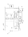
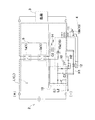
以下、本発明を具体化した実施の形態を、図面を参照して詳細に説明する。図1は本発明に係る直流3路スイッチ装置の回路図であり、1は3路スイッチ(第1の3路スイッチ1a、第2の3路スイッチ1b)、2は直流電源、3は電灯等の直流の負荷、4はアーク放電の発生を防止するためのアーク制御回路である。負荷3に電力を供給する主電路Lは、正極側電路L1と負極側電路L2の2本の電路で構成され、第1の3路スイッチ1aと第2の3路スイッチ1bとは直列接続されて負荷操作路5を形成している。
また、正極側電路L1は電源2と負荷3とが接点等を介さず直接接続される一方で、負極側電路L2はアーク制御回路4を介して電源2と負荷3とが接続され、負荷操作路5は正極側電路L1の途中とアーク制御回路4を介して負極側電路L2に接続され、負荷3に対して並列に配置されている。
DESCRIPTION OF THE PREFERRED EMBODIMENTS Embodiments embodying the present invention will be described below in detail with reference to the drawings. FIG. 1 is a circuit diagram of a DC three-way switch device according to the present invention, wherein 1 is a three-way switch (first three-
Further, the positive side electric circuit L1 is directly connected to the
アーク制御回路4は、負極側電路L2に介在された半導体スイッチとしてのMOSFET(以下、単に「FET」とする。)10と、このFET10の負荷側に直列に配置された第1のリレー11と、FET10に並列に配置されて第1のリレー11に対しては直列に配置された第2のリレー12と、FET10のチャタリングを防止するためのチャタリング防止回路13と、第1及び第2のリレー11,12を駆動するための電源回路としてのDC/DCコンバータ14と、第2のリレー12をオフ動作させるためのフォトカプラ15(発光部15a,受光部15b)とを有している。
The
尚、負荷操作路5の負極側電路L2との接続部は、FET10のゲートであり、3路スイッチ1の操作でFET10が操作される。また、第2のリレー12を備えた回路を負極側電路L2のバイパス電路H1、FET10を備えた回路を補助電路H2として説明する。
In addition, the connection part with the negative electrode side electric circuit L2 of the
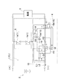
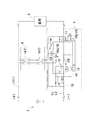
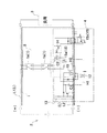
上記の如く構成された直流3路スイッチ装置の動作は以下のようである。負荷3のオン/オフ操作は従来の操作と同様であり、双方の3路スイッチ1a,1bがオン状態(負荷操作路5が導通状態)にあると負荷3もオンし、一方の3路スイッチ1を操作して負荷操作路5が断路すると負荷3はオフする。図2〜4はオフ動作の流れを示す説明図、図5〜7はオン動作の流れを示す説明図であり、この図2〜7を参照して説明する。
The operation of the DC three-way switch device configured as described above is as follows. The on / off operation of the
負荷操作路5が導通状態にあると、DC/DCコンバータ14がオンして所定の電圧を出力する。また、フォトカプラ15がオンするため、第1のリレー11及び第2のリレー12はオンし、主電路Lは閉路して直流電源2の正極から正極側電路L1を介して負荷3に流れる負荷電流は、負極側電路L2の第1のリレー11、バイパス電路H1を介して直流電源2の負極に流れる。図2はこのオン状態を示し、破線で示すiは負荷電流の流れを示している。
When the
この状態から、一方の直流3路スイッチ1を操作して負荷操作路5をオフ操作すると以下の様に動作する。一方の3路スイッチ1を操作してオフ操作すると、負荷操作路5が非導通となり、DC/DCコンバータ14及びフォトカプラ15がオフする。但し、DC/DCコンバータ14は遅延動作用コンデンサC2の作用により、フォトカプラ15より遅れてオフ動作する。図3はこの状態を示し、負荷操作路5のオフ操作を受けてまず第2のリレー12がオフするが、負極側電路L2の負荷電流iの通電路がバイパス電路H1から補助電路H2に変わるだけで、主電路Lの通電は維持されて負荷3のオン状態は継続する。
From this state, when one of the DC three-
その後、オフ操作を受けてチャタリング防止回路13が作動してFET10を確実にオフ操作する。図4は、この状態を示している。また、その直後に遅延動作用コンデンサC2の充電電荷が放出されることで、DC/DCコンバータ14がオフして第1のリレー11もオフする。こうして、主電路Lは遮断されて負荷3がオフとなる。図1は、この状態を示している。
Thereafter, the
次に、オン操作を受けた回路動作を説明する。任意の一方の直流3路スイッチ1を操作して、非導通状態にある負荷操作路5を導通状態に変化させると、まずFET10がオンする。
同時にフォトカプラ15もオンするが、DC/DCコンバータ14のオン動作まで一定の時間を要するため、第1のリレー11は直ぐにはオンしない。従って、第1のリレー11の動作に依存する第2のリレー12もオンしない。この状態が図5の状態である。
その後、DC/DCコンバータ14が動作を開始することで、第1のリレー11がオンする。この結果、図6に示すように補助電路H2を使用した負極側電路L2が導通状態となり、負荷電流iが流れ始める。更にその直後、第1のリレー11のオン動作を受けて第2のリレー12がオンするため、図7に示すように負荷電流iの通電路が補助電路H2からバイパス電路H1に移行して、負荷3への通電が継続される。
Next, the circuit operation that has undergone the ON operation will be described. When any one of the DC three-
At the same time, the
Thereafter, when the DC /
このように、一対の3路スイッチ1a,1bは、負荷3に対して並列に配置されるため、負荷3に通電する電流によらず3路スイッチ1に流れる電流を僅かにでき、3路スイッチ1の接点にアーク放電が殆ど発生しないよう構成できる。よって、接点の長寿命化を図ることができ、既存の交流3路スイッチの使用が可能となる。更に、FET10は、2つの3路スイッチ1a,1bに対して1つで良く低コスト化を図ることができる。
また、FET10に並列に接続された第2のリレー12は、3路スイッチ1のオン/オフ操作を受けてオン/オフする。即ち、負荷操作路5が導通状態のときオン状態にある。よって、FET10がオンの時第2のリレー12もオンであり、負荷電流をFET10ではなく第2のリレー12を介させることができ、FET10の電力消費による発熱を防止できる。更に、オフ操作して負荷操作路5が断路したら、第1のリレー11もオフするため、主電路Lは確実に遮断され、負荷3に電圧が印加され続けるようなことがない。
加えて、チャタリング防止回路13を設けたことで、オフ操作時にFET10が不安定な動作をすることが無く、負荷3を確実にオフ操作できる。
Thus, since the pair of three-
The
In addition, since the
1(1a,1b)・・3路スイッチ、2・・直流電源、3・・負荷、4・・アーク制御回路、5・・負荷操作路、10・・FET(半導体スイッチ)、11・・第1のリレー、13・・第2のリレー、13・・チャタリング防止回路、15・・フォトカプラ、L1・・正極側電路、L2・・負極側電路、C2・・遅延動作用コンデンサ(遅延手段)。
1 (1a, 1b) ··· 3-
Claims (3)
負荷に電力を供給する正極側電路及び負極側電路から成る主電路のうちの負極側電路に、半導体スイッチを介在させたアーク制御回路が設けられる一方、
前記一対の3路スイッチは直列に接続されて負荷操作路を形成し、当該負荷操作路の一端は前記半導体スイッチのゲートに接続されて、負荷操作路全体は前記負荷に対して並列に配置されて成り、
前記一対の3路スイッチにより、前記半導体スイッチをオン/オフ操作することで前記負荷をオン/オフすることを特徴とする直流3路スイッチ装置。 A direct-current three-way switch device for turning on / off a common direct-current load from two locations by a pair of three-way switches,
While an arc control circuit with a semiconductor switch interposed is provided on the negative electrode side of the main circuit consisting of a positive electrode circuit and a negative electrode circuit for supplying power to the load,
The pair of three-way switches are connected in series to form a load operation path, one end of the load operation path is connected to the gate of the semiconductor switch, and the entire load operation path is arranged in parallel to the load. And
A direct current three-way switch device, wherein the load is turned on / off by turning on / off the semiconductor switch by the pair of three-way switches.
前記半導体スイッチに並列に配置され、且つ前記第1のリレーに直列に配置された第2のリレーと、
前記第1のリレーのオフ動作を前記第2のリレーのオフ動作より遅延させる遅延手段とを有し、
前記1のリレー及び前記第2のリレーは、前記3路スイッチのオン/オフ操作を受けてオン/オフすることを特徴とする請求項1記載の直流3路スイッチ装置。 The arc control circuit includes a first relay arranged in series on the load side of the semiconductor switch;
A second relay disposed in parallel with the semiconductor switch and disposed in series with the first relay;
Delay means for delaying the off operation of the first relay from the off operation of the second relay;
2. The DC three-way switch device according to claim 1, wherein the first relay and the second relay are turned on / off in response to an on / off operation of the three-way switch.
Priority Applications (1)
| Application Number | Priority Date | Filing Date | Title |
|---|---|---|---|
| JP2016079750A JP2017191682A (en) | 2016-04-12 | 2016-04-12 | DC 3-way switch device |
Applications Claiming Priority (1)
| Application Number | Priority Date | Filing Date | Title |
|---|---|---|---|
| JP2016079750A JP2017191682A (en) | 2016-04-12 | 2016-04-12 | DC 3-way switch device |
Publications (1)
| Publication Number | Publication Date |
|---|---|
| JP2017191682A true JP2017191682A (en) | 2017-10-19 |
Family
ID=60085218
Family Applications (1)
| Application Number | Title | Priority Date | Filing Date |
|---|---|---|---|
| JP2016079750A Pending JP2017191682A (en) | 2016-04-12 | 2016-04-12 | DC 3-way switch device |
Country Status (1)
| Country | Link |
|---|---|
| JP (1) | JP2017191682A (en) |
Cited By (1)
| Publication number | Priority date | Publication date | Assignee | Title |
|---|---|---|---|---|
| US12614686B2 (en) | 2022-11-11 | 2026-04-28 | Enphase Energy, Inc. | Arc-free hybrid relay |
Citations (3)
| Publication number | Priority date | Publication date | Assignee | Title |
|---|---|---|---|---|
| JPS5268116U (en) * | 1975-11-14 | 1977-05-20 | ||
| US5652688A (en) * | 1995-09-12 | 1997-07-29 | Schweitzer Engineering Laboratories, Inc. | Hybrid circuit using miller effect for protection of electrical contacts from arcing |
| JP2012028193A (en) * | 2010-07-23 | 2012-02-09 | Matsuo Hirofumi | Dc switch |
-
2016
- 2016-04-12 JP JP2016079750A patent/JP2017191682A/en active Pending
Patent Citations (3)
| Publication number | Priority date | Publication date | Assignee | Title |
|---|---|---|---|---|
| JPS5268116U (en) * | 1975-11-14 | 1977-05-20 | ||
| US5652688A (en) * | 1995-09-12 | 1997-07-29 | Schweitzer Engineering Laboratories, Inc. | Hybrid circuit using miller effect for protection of electrical contacts from arcing |
| JP2012028193A (en) * | 2010-07-23 | 2012-02-09 | Matsuo Hirofumi | Dc switch |
Cited By (1)
| Publication number | Priority date | Publication date | Assignee | Title |
|---|---|---|---|---|
| US12614686B2 (en) | 2022-11-11 | 2026-04-28 | Enphase Energy, Inc. | Arc-free hybrid relay |
Similar Documents
| Publication | Publication Date | Title |
|---|---|---|
| JP5881511B2 (en) | Power outlet for DC distribution | |
| CN102122839B (en) | Electric-dazzling prevention auxiliary power supply in low-voltage alternating current control loop and power supply method thereof | |
| KR102093112B1 (en) | Interrupt device for interrupting direct current | |
| JP2012248445A (en) | Switch | |
| WO2016194584A1 (en) | Dc circuit, dc power supply device, moving body, and power supply system | |
| JP2013214406A (en) | Circuit cut-off switch for dc circuit | |
| JP2014120364A (en) | Circuit breaker switch for dc circuit | |
| JP2014038775A (en) | Circuit breaking switch for dc circuit | |
| KR20120137385A (en) | Hybrid relay | |
| CN107482760B (en) | Switching device | |
| JP2014216056A (en) | Dc circuit breaker device | |
| WO2018131307A1 (en) | Arc-suppressing device | |
| JP2017191682A (en) | DC 3-way switch device | |
| KR20150142546A (en) | Electromagnetic contactor and control method thereof | |
| JP2021520600A (en) | A disconnecting device for cutting off the direct current in the current path, and an in-vehicle power supply system for automobiles. | |
| JP6143615B2 (en) | DC switch | |
| RU2343580C1 (en) | Electromagnetic drive | |
| JP6302663B2 (en) | DC switch | |
| PH12022551203A1 (en) | Charging base and charging system | |
| TWI597920B (en) | Switch Device | |
| JP2017135074A (en) | DC three-way switch | |
| WO2022152589A1 (en) | Emergency led driver | |
| JP2017126467A (en) | DC switch for wall | |
| JP4381711B2 (en) | Method for opening and closing circuit breaker synchronously in distribution system and device for implementing this method | |
| CN102684137A (en) | System and method for safely powering on/off high-voltage circuits |
Legal Events
| Date | Code | Title | Description |
|---|---|---|---|
| A621 | Written request for application examination |
Free format text: JAPANESE INTERMEDIATE CODE: A621 Effective date: 20190221 |
|
| A977 | Report on retrieval |
Free format text: JAPANESE INTERMEDIATE CODE: A971007 Effective date: 20191219 |
|
| A131 | Notification of reasons for refusal |
Free format text: JAPANESE INTERMEDIATE CODE: A131 Effective date: 20191224 |
|
| A02 | Decision of refusal |
Free format text: JAPANESE INTERMEDIATE CODE: A02 Effective date: 20200623 |