JP2017191893A - Printed wiring board - Google Patents
Printed wiring board Download PDFInfo
- Publication number
- JP2017191893A JP2017191893A JP2016081448A JP2016081448A JP2017191893A JP 2017191893 A JP2017191893 A JP 2017191893A JP 2016081448 A JP2016081448 A JP 2016081448A JP 2016081448 A JP2016081448 A JP 2016081448A JP 2017191893 A JP2017191893 A JP 2017191893A
- Authority
- JP
- Japan
- Prior art keywords
- layer
- conductor
- solder resist
- wiring board
- printed wiring
- Prior art date
- Legal status (The legal status is an assumption and is not a legal conclusion. Google has not performed a legal analysis and makes no representation as to the accuracy of the status listed.)
- Pending
Links
- 239000004020 conductor Substances 0.000 claims abstract description 137
- 229910000679 solder Inorganic materials 0.000 claims abstract description 75
- 239000010949 copper Substances 0.000 claims abstract description 38
- RYGMFSIKBFXOCR-UHFFFAOYSA-N Copper Chemical compound [Cu] RYGMFSIKBFXOCR-UHFFFAOYSA-N 0.000 claims abstract description 37
- 229910052802 copper Inorganic materials 0.000 claims abstract description 36
- IJGRMHOSHXDMSA-UHFFFAOYSA-N Atomic nitrogen Chemical compound N#N IJGRMHOSHXDMSA-UHFFFAOYSA-N 0.000 claims abstract description 14
- 229910052757 nitrogen Inorganic materials 0.000 claims abstract description 9
- 239000000758 substrate Substances 0.000 claims abstract description 8
- 239000000463 material Substances 0.000 claims description 19
- 230000032798 delamination Effects 0.000 abstract description 2
- 239000010410 layer Substances 0.000 description 252
- 238000000034 method Methods 0.000 description 32
- 239000003822 epoxy resin Substances 0.000 description 22
- 239000000203 mixture Substances 0.000 description 22
- 229920000647 polyepoxide Polymers 0.000 description 22
- 229920005989 resin Polymers 0.000 description 22
- 239000011347 resin Substances 0.000 description 22
- 239000007788 liquid Substances 0.000 description 21
- 239000011342 resin composition Substances 0.000 description 18
- 239000002243 precursor Substances 0.000 description 17
- 239000002585 base Substances 0.000 description 16
- -1 glycol ethers Chemical class 0.000 description 16
- 238000009713 electroplating Methods 0.000 description 15
- 229920001187 thermosetting polymer Polymers 0.000 description 15
- 239000007864 aqueous solution Substances 0.000 description 13
- XLYOFNOQVPJJNP-UHFFFAOYSA-N water Substances O XLYOFNOQVPJJNP-UHFFFAOYSA-N 0.000 description 13
- KAESVJOAVNADME-UHFFFAOYSA-N 1H-pyrrole Natural products C=1C=CNC=1 KAESVJOAVNADME-UHFFFAOYSA-N 0.000 description 12
- 238000001723 curing Methods 0.000 description 12
- 239000003795 chemical substances by application Substances 0.000 description 11
- JPVYNHNXODAKFH-UHFFFAOYSA-N Cu2+ Chemical compound [Cu+2] JPVYNHNXODAKFH-UHFFFAOYSA-N 0.000 description 10
- RAXXELZNTBOGNW-UHFFFAOYSA-N imidazole Natural products C1=CNC=N1 RAXXELZNTBOGNW-UHFFFAOYSA-N 0.000 description 9
- 238000004519 manufacturing process Methods 0.000 description 9
- 229920003986 novolac Polymers 0.000 description 9
- 239000011248 coating agent Substances 0.000 description 8
- 238000000576 coating method Methods 0.000 description 8
- 239000012792 core layer Substances 0.000 description 8
- 239000000243 solution Substances 0.000 description 8
- 239000002904 solvent Substances 0.000 description 8
- PXHVJJICTQNCMI-UHFFFAOYSA-N Nickel Chemical compound [Ni] PXHVJJICTQNCMI-UHFFFAOYSA-N 0.000 description 7
- 150000001875 compounds Chemical class 0.000 description 7
- 239000003999 initiator Substances 0.000 description 7
- 125000004433 nitrogen atom Chemical group N* 0.000 description 7
- 239000002335 surface treatment layer Substances 0.000 description 7
- VEXZGXHMUGYJMC-UHFFFAOYSA-N Hydrochloric acid Chemical compound Cl VEXZGXHMUGYJMC-UHFFFAOYSA-N 0.000 description 6
- QAOWNCQODCNURD-UHFFFAOYSA-N Sulfuric acid Chemical compound OS(O)(=O)=O QAOWNCQODCNURD-UHFFFAOYSA-N 0.000 description 6
- LNEPOXFFQSENCJ-UHFFFAOYSA-N haloperidol Chemical compound C1CC(O)(C=2C=CC(Cl)=CC=2)CCN1CCCC(=O)C1=CC=C(F)C=C1 LNEPOXFFQSENCJ-UHFFFAOYSA-N 0.000 description 6
- 229920000642 polymer Polymers 0.000 description 6
- 238000001035 drying Methods 0.000 description 5
- 239000003504 photosensitizing agent Substances 0.000 description 5
- 238000007747 plating Methods 0.000 description 5
- KLSJWNVTNUYHDU-UHFFFAOYSA-N Amitrole Chemical group NC1=NC=NN1 KLSJWNVTNUYHDU-UHFFFAOYSA-N 0.000 description 4
- QGZKDVFQNNGYKY-UHFFFAOYSA-N Ammonia Chemical compound N QGZKDVFQNNGYKY-UHFFFAOYSA-N 0.000 description 4
- ISWSIDIOOBJBQZ-UHFFFAOYSA-N Phenol Chemical compound OC1=CC=CC=C1 ISWSIDIOOBJBQZ-UHFFFAOYSA-N 0.000 description 4
- 238000004833 X-ray photoelectron spectroscopy Methods 0.000 description 4
- 230000002378 acidificating effect Effects 0.000 description 4
- 238000006243 chemical reaction Methods 0.000 description 4
- 229910001431 copper ion Inorganic materials 0.000 description 4
- 239000012530 fluid Substances 0.000 description 4
- 229910052751 metal Inorganic materials 0.000 description 4
- 239000002184 metal Substances 0.000 description 4
- 239000003960 organic solvent Substances 0.000 description 4
- 230000003647 oxidation Effects 0.000 description 4
- 238000007254 oxidation reaction Methods 0.000 description 4
- 238000005476 soldering Methods 0.000 description 4
- 239000000126 substance Substances 0.000 description 4
- QTBSBXVTEAMEQO-UHFFFAOYSA-N Acetic acid Chemical compound CC(O)=O QTBSBXVTEAMEQO-UHFFFAOYSA-N 0.000 description 3
- OKKJLVBELUTLKV-UHFFFAOYSA-N Methanol Chemical compound OC OKKJLVBELUTLKV-UHFFFAOYSA-N 0.000 description 3
- KWYUFKZDYYNOTN-UHFFFAOYSA-M Potassium hydroxide Chemical compound [OH-].[K+] KWYUFKZDYYNOTN-UHFFFAOYSA-M 0.000 description 3
- HEMHJVSKTPXQMS-UHFFFAOYSA-M Sodium hydroxide Chemical compound [OH-].[Na+] HEMHJVSKTPXQMS-UHFFFAOYSA-M 0.000 description 3
- 125000003118 aryl group Chemical group 0.000 description 3
- 125000003700 epoxy group Chemical group 0.000 description 3
- 239000011256 inorganic filler Substances 0.000 description 3
- 229910003475 inorganic filler Inorganic materials 0.000 description 3
- 239000011229 interlayer Substances 0.000 description 3
- 239000013067 intermediate product Substances 0.000 description 3
- 229910052759 nickel Inorganic materials 0.000 description 3
- 150000007524 organic acids Chemical class 0.000 description 3
- 238000000016 photochemical curing Methods 0.000 description 3
- 238000005554 pickling Methods 0.000 description 3
- 238000007788 roughening Methods 0.000 description 3
- 239000004065 semiconductor Substances 0.000 description 3
- 238000005406 washing Methods 0.000 description 3
- KJUGUADJHNHALS-UHFFFAOYSA-N 1H-tetrazole Chemical compound C=1N=NNN=1 KJUGUADJHNHALS-UHFFFAOYSA-N 0.000 description 2
- HZAXFHJVJLSVMW-UHFFFAOYSA-N 2-Aminoethan-1-ol Chemical compound NCCO HZAXFHJVJLSVMW-UHFFFAOYSA-N 0.000 description 2
- QTWJRLJHJPIABL-UHFFFAOYSA-N 2-methylphenol;3-methylphenol;4-methylphenol Chemical compound CC1=CC=C(O)C=C1.CC1=CC=CC(O)=C1.CC1=CC=CC=C1O QTWJRLJHJPIABL-UHFFFAOYSA-N 0.000 description 2
- VVBLNCFGVYUYGU-UHFFFAOYSA-N 4,4'-Bis(dimethylamino)benzophenone Chemical compound C1=CC(N(C)C)=CC=C1C(=O)C1=CC=C(N(C)C)C=C1 VVBLNCFGVYUYGU-UHFFFAOYSA-N 0.000 description 2
- OKTJSMMVPCPJKN-UHFFFAOYSA-N Carbon Chemical compound [C] OKTJSMMVPCPJKN-UHFFFAOYSA-N 0.000 description 2
- LFQSCWFLJHTTHZ-UHFFFAOYSA-N Ethanol Chemical compound CCO LFQSCWFLJHTTHZ-UHFFFAOYSA-N 0.000 description 2
- AEMRFAOFKBGASW-UHFFFAOYSA-N Glycolic acid Chemical compound OCC(O)=O AEMRFAOFKBGASW-UHFFFAOYSA-N 0.000 description 2
- MHAJPDPJQMAIIY-UHFFFAOYSA-N Hydrogen peroxide Chemical compound OO MHAJPDPJQMAIIY-UHFFFAOYSA-N 0.000 description 2
- CERQOIWHTDAKMF-UHFFFAOYSA-N Methacrylic acid Chemical compound CC(=C)C(O)=O CERQOIWHTDAKMF-UHFFFAOYSA-N 0.000 description 2
- UFWIBTONFRDIAS-UHFFFAOYSA-N Naphthalene Chemical compound C1=CC=CC2=CC=CC=C21 UFWIBTONFRDIAS-UHFFFAOYSA-N 0.000 description 2
- GRYLNZFGIOXLOG-UHFFFAOYSA-N Nitric acid Chemical compound O[N+]([O-])=O GRYLNZFGIOXLOG-UHFFFAOYSA-N 0.000 description 2
- WTKZEGDFNFYCGP-UHFFFAOYSA-N Pyrazole Chemical group C=1C=NNC=1 WTKZEGDFNFYCGP-UHFFFAOYSA-N 0.000 description 2
- VYPSYNLAJGMNEJ-UHFFFAOYSA-N Silicium dioxide Chemical compound O=[Si]=O VYPSYNLAJGMNEJ-UHFFFAOYSA-N 0.000 description 2
- ATJFFYVFTNAWJD-UHFFFAOYSA-N Tin Chemical compound [Sn] ATJFFYVFTNAWJD-UHFFFAOYSA-N 0.000 description 2
- HCHKCACWOHOZIP-UHFFFAOYSA-N Zinc Chemical compound [Zn] HCHKCACWOHOZIP-UHFFFAOYSA-N 0.000 description 2
- 125000002723 alicyclic group Chemical group 0.000 description 2
- 150000001412 amines Chemical class 0.000 description 2
- 229910021529 ammonia Inorganic materials 0.000 description 2
- 150000008365 aromatic ketones Chemical class 0.000 description 2
- TZCXTZWJZNENPQ-UHFFFAOYSA-L barium sulfate Chemical compound [Ba+2].[O-]S([O-])(=O)=O TZCXTZWJZNENPQ-UHFFFAOYSA-L 0.000 description 2
- 230000005540 biological transmission Effects 0.000 description 2
- 230000015572 biosynthetic process Effects 0.000 description 2
- IISBACLAFKSPIT-UHFFFAOYSA-N bisphenol A Chemical compound C=1C=C(O)C=CC=1C(C)(C)C1=CC=C(O)C=C1 IISBACLAFKSPIT-UHFFFAOYSA-N 0.000 description 2
- PXKLMJQFEQBVLD-UHFFFAOYSA-N bisphenol F Chemical compound C1=CC(O)=CC=C1CC1=CC=C(O)C=C1 PXKLMJQFEQBVLD-UHFFFAOYSA-N 0.000 description 2
- 229910052799 carbon Inorganic materials 0.000 description 2
- 150000001879 copper Chemical class 0.000 description 2
- ORTQZVOHEJQUHG-UHFFFAOYSA-L copper(II) chloride Chemical compound Cl[Cu]Cl ORTQZVOHEJQUHG-UHFFFAOYSA-L 0.000 description 2
- 229930003836 cresol Natural products 0.000 description 2
- ZUOUZKKEUPVFJK-UHFFFAOYSA-N diphenyl Chemical compound C1=CC=CC=C1C1=CC=CC=C1 ZUOUZKKEUPVFJK-UHFFFAOYSA-N 0.000 description 2
- 239000012153 distilled water Substances 0.000 description 2
- 230000000694 effects Effects 0.000 description 2
- 238000007772 electroless plating Methods 0.000 description 2
- 238000005530 etching Methods 0.000 description 2
- LYCAIKOWRPUZTN-UHFFFAOYSA-N ethylene glycol Natural products OCCO LYCAIKOWRPUZTN-UHFFFAOYSA-N 0.000 description 2
- JEGUKCSWCFPDGT-UHFFFAOYSA-N h2o hydrate Chemical compound O.O JEGUKCSWCFPDGT-UHFFFAOYSA-N 0.000 description 2
- WGCNASOHLSPBMP-UHFFFAOYSA-N hydroxyacetaldehyde Natural products OCC=O WGCNASOHLSPBMP-UHFFFAOYSA-N 0.000 description 2
- 238000007654 immersion Methods 0.000 description 2
- JEIPFZHSYJVQDO-UHFFFAOYSA-N iron(III) oxide Inorganic materials O=[Fe]O[Fe]=O JEIPFZHSYJVQDO-UHFFFAOYSA-N 0.000 description 2
- JVTAAEKCZFNVCJ-UHFFFAOYSA-N lactic acid Chemical compound CC(O)C(O)=O JVTAAEKCZFNVCJ-UHFFFAOYSA-N 0.000 description 2
- 238000010030 laminating Methods 0.000 description 2
- BDAGIHXWWSANSR-UHFFFAOYSA-N methanoic acid Natural products OC=O BDAGIHXWWSANSR-UHFFFAOYSA-N 0.000 description 2
- 229910017604 nitric acid Inorganic materials 0.000 description 2
- 238000002360 preparation method Methods 0.000 description 2
- 230000002265 prevention Effects 0.000 description 2
- 238000005507 spraying Methods 0.000 description 2
- 239000002344 surface layer Substances 0.000 description 2
- 238000004381 surface treatment Methods 0.000 description 2
- 229910052725 zinc Inorganic materials 0.000 description 2
- 239000011701 zinc Substances 0.000 description 2
- OUPZKGBUJRBPGC-UHFFFAOYSA-N 1,3,5-tris(oxiran-2-ylmethyl)-1,3,5-triazinane-2,4,6-trione Chemical compound O=C1N(CC2OC2)C(=O)N(CC2OC2)C(=O)N1CC1CO1 OUPZKGBUJRBPGC-UHFFFAOYSA-N 0.000 description 1
- XQUPVDVFXZDTLT-UHFFFAOYSA-N 1-[4-[[4-(2,5-dioxopyrrol-1-yl)phenyl]methyl]phenyl]pyrrole-2,5-dione Chemical compound O=C1C=CC(=O)N1C(C=C1)=CC=C1CC1=CC=C(N2C(C=CC2=O)=O)C=C1 XQUPVDVFXZDTLT-UHFFFAOYSA-N 0.000 description 1
- HECLRDQVFMWTQS-RGOKHQFPSA-N 1755-01-7 Chemical compound C1[C@H]2[C@@H]3CC=C[C@@H]3[C@@H]1C=C2 HECLRDQVFMWTQS-RGOKHQFPSA-N 0.000 description 1
- QWENRTYMTSOGBR-UHFFFAOYSA-N 1H-1,2,3-Triazole Chemical compound C=1C=NNN=1 QWENRTYMTSOGBR-UHFFFAOYSA-N 0.000 description 1
- SMZOUWXMTYCWNB-UHFFFAOYSA-N 2-(2-methoxy-5-methylphenyl)ethanamine Chemical compound COC1=CC=C(C)C=C1CCN SMZOUWXMTYCWNB-UHFFFAOYSA-N 0.000 description 1
- NIXOWILDQLNWCW-UHFFFAOYSA-N 2-Propenoic acid Natural products OC(=O)C=C NIXOWILDQLNWCW-UHFFFAOYSA-N 0.000 description 1
- OSWFIVFLDKOXQC-UHFFFAOYSA-N 4-(3-methoxyphenyl)aniline Chemical compound COC1=CC=CC(C=2C=CC(N)=CC=2)=C1 OSWFIVFLDKOXQC-UHFFFAOYSA-N 0.000 description 1
- NSPMIYGKQJPBQR-UHFFFAOYSA-N 4H-1,2,4-triazole Chemical compound C=1N=CNN=1 NSPMIYGKQJPBQR-UHFFFAOYSA-N 0.000 description 1
- NIXOWILDQLNWCW-UHFFFAOYSA-M Acrylate Chemical compound [O-]C(=O)C=C NIXOWILDQLNWCW-UHFFFAOYSA-M 0.000 description 1
- QPLDLSVMHZLSFG-UHFFFAOYSA-N Copper oxide Chemical compound [Cu]=O QPLDLSVMHZLSFG-UHFFFAOYSA-N 0.000 description 1
- 239000005751 Copper oxide Substances 0.000 description 1
- 229910000570 Cupronickel Inorganic materials 0.000 description 1
- 206010034972 Photosensitivity reaction Diseases 0.000 description 1
- 229910001297 Zn alloy Inorganic materials 0.000 description 1
- QXZUUHYBWMWJHK-UHFFFAOYSA-N [Co].[Ni] Chemical compound [Co].[Ni] QXZUUHYBWMWJHK-UHFFFAOYSA-N 0.000 description 1
- VDGMIGHRDCJLMN-UHFFFAOYSA-N [Cu].[Co].[Ni] Chemical compound [Cu].[Co].[Ni] VDGMIGHRDCJLMN-UHFFFAOYSA-N 0.000 description 1
- 235000011054 acetic acid Nutrition 0.000 description 1
- 239000002253 acid Substances 0.000 description 1
- 150000008065 acid anhydrides Chemical class 0.000 description 1
- 125000003647 acryloyl group Chemical group O=C([*])C([H])=C([H])[H] 0.000 description 1
- 150000008044 alkali metal hydroxides Chemical class 0.000 description 1
- 150000001413 amino acids Chemical class 0.000 description 1
- 238000004458 analytical method Methods 0.000 description 1
- 150000003934 aromatic aldehydes Chemical class 0.000 description 1
- 239000012298 atmosphere Substances 0.000 description 1
- 150000008366 benzophenones Chemical class 0.000 description 1
- 239000004305 biphenyl Substances 0.000 description 1
- 235000010290 biphenyl Nutrition 0.000 description 1
- ZCDOYSPFYFSLEW-UHFFFAOYSA-N chromate(2-) Chemical compound [O-][Cr]([O-])(=O)=O ZCDOYSPFYFSLEW-UHFFFAOYSA-N 0.000 description 1
- YOCUPQPZWBBYIX-UHFFFAOYSA-N copper nickel Chemical compound [Ni].[Cu] YOCUPQPZWBBYIX-UHFFFAOYSA-N 0.000 description 1
- 229910000431 copper oxide Inorganic materials 0.000 description 1
- 229910000365 copper sulfate Inorganic materials 0.000 description 1
- TVZPLCNGKSPOJA-UHFFFAOYSA-N copper zinc Chemical compound [Cu].[Zn] TVZPLCNGKSPOJA-UHFFFAOYSA-N 0.000 description 1
- XTVVROIMIGLXTD-UHFFFAOYSA-N copper(II) nitrate Chemical compound [Cu+2].[O-][N+]([O-])=O.[O-][N+]([O-])=O XTVVROIMIGLXTD-UHFFFAOYSA-N 0.000 description 1
- ARUVKPQLZAKDPS-UHFFFAOYSA-L copper(II) sulfate Chemical compound [Cu+2].[O-][S+2]([O-])([O-])[O-] ARUVKPQLZAKDPS-UHFFFAOYSA-L 0.000 description 1
- OPQARKPSCNTWTJ-UHFFFAOYSA-L copper(ii) acetate Chemical compound [Cu+2].CC([O-])=O.CC([O-])=O OPQARKPSCNTWTJ-UHFFFAOYSA-L 0.000 description 1
- HFDWIMBEIXDNQS-UHFFFAOYSA-L copper;diformate Chemical compound [Cu+2].[O-]C=O.[O-]C=O HFDWIMBEIXDNQS-UHFFFAOYSA-L 0.000 description 1
- 238000010586 diagram Methods 0.000 description 1
- SBZXBUIDTXKZTM-UHFFFAOYSA-N diglyme Chemical compound COCCOCCOC SBZXBUIDTXKZTM-UHFFFAOYSA-N 0.000 description 1
- 235000019253 formic acid Nutrition 0.000 description 1
- 229910052737 gold Inorganic materials 0.000 description 1
- 239000010931 gold Substances 0.000 description 1
- MSNOMDLPLDYDME-UHFFFAOYSA-N gold nickel Chemical compound [Ni].[Au] MSNOMDLPLDYDME-UHFFFAOYSA-N 0.000 description 1
- 238000010438 heat treatment Methods 0.000 description 1
- XEMZLVDIUVCKGL-UHFFFAOYSA-N hydrogen peroxide;sulfuric acid Chemical compound OO.OS(O)(=O)=O XEMZLVDIUVCKGL-UHFFFAOYSA-N 0.000 description 1
- 125000002887 hydroxy group Chemical group [H]O* 0.000 description 1
- 229910052500 inorganic mineral Inorganic materials 0.000 description 1
- FBAFATDZDUQKNH-UHFFFAOYSA-M iron chloride Chemical compound [Cl-].[Fe] FBAFATDZDUQKNH-UHFFFAOYSA-M 0.000 description 1
- 230000001678 irradiating effect Effects 0.000 description 1
- 239000004310 lactic acid Substances 0.000 description 1
- 235000014655 lactic acid Nutrition 0.000 description 1
- 239000011707 mineral Substances 0.000 description 1
- 230000004048 modification Effects 0.000 description 1
- 238000012986 modification Methods 0.000 description 1
- QELJHCBNGDEXLD-UHFFFAOYSA-N nickel zinc Chemical compound [Ni].[Zn] QELJHCBNGDEXLD-UHFFFAOYSA-N 0.000 description 1
- 230000001590 oxidative effect Effects 0.000 description 1
- 239000002245 particle Substances 0.000 description 1
- JRKICGRDRMAZLK-UHFFFAOYSA-L peroxydisulfate Chemical compound [O-]S(=O)(=O)OOS([O-])(=O)=O JRKICGRDRMAZLK-UHFFFAOYSA-L 0.000 description 1
- 239000005011 phenolic resin Substances 0.000 description 1
- 150000002989 phenols Chemical class 0.000 description 1
- OFNHPGDEEMZPFG-UHFFFAOYSA-N phosphanylidynenickel Chemical compound [P].[Ni] OFNHPGDEEMZPFG-UHFFFAOYSA-N 0.000 description 1
- 238000006552 photochemical reaction Methods 0.000 description 1
- 230000036211 photosensitivity Effects 0.000 description 1
- 230000000704 physical effect Effects 0.000 description 1
- 238000005498 polishing Methods 0.000 description 1
- 229920003192 poly(bis maleimide) Polymers 0.000 description 1
- 229920001225 polyester resin Polymers 0.000 description 1
- 239000004645 polyester resin Substances 0.000 description 1
- 229920001721 polyimide Polymers 0.000 description 1
- 239000009719 polyimide resin Substances 0.000 description 1
- 229920005672 polyolefin resin Polymers 0.000 description 1
- 229920001955 polyphenylene ether Polymers 0.000 description 1
- 230000001376 precipitating effect Effects 0.000 description 1
- 239000003755 preservative agent Substances 0.000 description 1
- 230000002335 preservative effect Effects 0.000 description 1
- 239000000047 product Substances 0.000 description 1
- BDERNNFJNOPAEC-UHFFFAOYSA-N propan-1-ol Chemical compound CCCO BDERNNFJNOPAEC-UHFFFAOYSA-N 0.000 description 1
- 230000001681 protective effect Effects 0.000 description 1
- 239000011241 protective layer Substances 0.000 description 1
- 239000000377 silicon dioxide Substances 0.000 description 1
- 239000002356 single layer Substances 0.000 description 1
- 238000004544 sputter deposition Methods 0.000 description 1
- 239000007858 starting material Substances 0.000 description 1
- 125000001424 substituent group Chemical group 0.000 description 1
- 239000000454 talc Substances 0.000 description 1
- 229910052623 talc Inorganic materials 0.000 description 1
- YRHRIQCWCFGUEQ-UHFFFAOYSA-N thioxanthen-9-one Chemical compound C1=CC=C2C(=O)C3=CC=CC=C3SC2=C1 YRHRIQCWCFGUEQ-UHFFFAOYSA-N 0.000 description 1
- 150000003852 triazoles Chemical group 0.000 description 1
- YFNKIDBQEZZDLK-UHFFFAOYSA-N triglyme Chemical compound COCCOCCOCCOC YFNKIDBQEZZDLK-UHFFFAOYSA-N 0.000 description 1
- 238000007740 vapor deposition Methods 0.000 description 1
Images


Landscapes
- Electric Connection Of Electric Components To Printed Circuits (AREA)
- Manufacturing Of Printed Wiring (AREA)
Abstract
Description
本発明はプリント配線基板に関する。 The present invention relates to a printed wiring board.
従来から、積層基材本体の表層に表面導体層のパターンを設け、該導体層をソルダーレジスト層(絶縁保護層)で被覆し、ソルダーレジスト層の一部に開口を形成して、導体層の一部を、半導体素子を実装するための実装パッドとして露出させたプリント配線基板が知られている。 Conventionally, a surface conductor layer pattern is provided on the surface layer of the laminated base body, the conductor layer is covered with a solder resist layer (insulating protective layer), an opening is formed in a part of the solder resist layer, A printed wiring board in which a part is exposed as a mounting pad for mounting a semiconductor element is known.
特許文献1では、金属と樹脂材料との接着方法において、所定構造のアゾールシラン化合物を含有する表面処理液を、銅などの金属の表面に接触させて化成皮膜を形成し、該化成皮膜を介して金属と樹脂材料とを接着することが開示されている。 In patent document 1, in the adhesion method of a metal and a resin material, a surface treatment liquid containing an azolesilane compound having a predetermined structure is brought into contact with the surface of a metal such as copper to form a chemical conversion film. It is disclosed to bond a metal and a resin material.
特許文献1では、電解めっき銅を含む表面導体層とソルダーレジスト層との密着のために、所定構造のアゾールシラン化合物を含有する表面処理液から構成される化成皮膜を用いることは開示されていない。 Patent Document 1 does not disclose the use of a chemical conversion film composed of a surface treatment liquid containing an azolesilane compound having a predetermined structure for adhesion between a surface conductor layer containing electrolytically plated copper and a solder resist layer. .
本発明者らは、電解めっき銅を含む表面導体層とソルダーレジスト層とを密着させる技術として十分に満足できる技術はこれまでに提供されておらず、依然として開発の必要性が高いと考えた。 The present inventors have not yet provided a sufficiently satisfactory technique as a technique for bringing a surface conductor layer containing electrolytically plated copper into close contact with a solder resist layer, and thought that the necessity for development is still high.
本発明は以下の発明を包含する。
本発明は、
導体層と絶縁層とをそれぞれ1層以上含む積層基材と、前記積層基材の表面の少なくとも一方に積層されたソルダーレジスト層とを有し、
前記積層基材は、前記導体層の少なくとも一部として、前記ソルダーレジスト層と接する表面に表面導体層を含む、プリント配線基板であって、
前記表面導体層は電解めっき銅を含み、
前記表面導体層と前記ソルダーレジスト層との間に接合層が介在しており、
前記接合層は、銅と窒素とを含む、厚さ20〜200nmの層である
プリント配線基板に関する。
The present invention includes the following inventions.
The present invention
A laminated base material including at least one conductor layer and an insulating layer, and a solder resist layer laminated on at least one of the surfaces of the laminated base material,
The laminated substrate is a printed wiring board including a surface conductor layer on a surface in contact with the solder resist layer as at least a part of the conductor layer,
The surface conductor layer includes electroplated copper,
A bonding layer is interposed between the surface conductor layer and the solder resist layer,
The bonding layer relates to a printed wiring board which is a layer having a thickness of 20 to 200 nm containing copper and nitrogen.
本発明のプリント配線基板の一実施形態によれば、電解めっき銅を含む表面導体層と前記ソルダーレジスト層とが銅と窒素とを含む接合層を介して密着することができ、表面導体層とソルダーレジスト層との間の層間剥離(ハロイング)が抑制される。 According to one embodiment of the printed wiring board of the present invention, the surface conductor layer containing electroplated copper and the solder resist layer can be in close contact with each other through a bonding layer containing copper and nitrogen, and the surface conductor layer and Delamination (haloing) between the solder resist layer is suppressed.
以下、本発明を具体化した実施の形態について、添付図面を参照しつつ詳細に説明する。
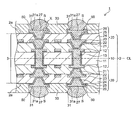
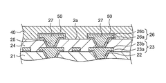
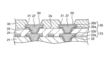
本発明の一実施形態に係るプリント配線基板1は、図1の概略断面図に示すように構成されている。
プリント配線基板1は、積層された導体層と絶縁層とをそれぞれ1以上含む。具体的にはプリント配線基板1はコア層10と、ビルドアップ層20と、ソルダーレジスト層30とを備えている。このプリント配線基板1は、ICチップ等の半導体素子をフリップチップ接続にて実装可能なパッケージ基板であり、且つ、半導体素子の実装後にマザーボード等の他のプリント配線基板に実装可能である。本実施形態のプリント配線基板1は多層積層プリント配線基板であり、全体としては板状又はフィルム状の形状を有する。また、図示しないが、本実施形態は、コア層10を含んでいないコアレス型プリント配線基板においても適用可能であることは当然である。
DESCRIPTION OF EXEMPLARY EMBODIMENTS Hereinafter, embodiments of the invention will be described in detail with reference to the accompanying drawings.
A printed wiring board 1 according to an embodiment of the present invention is configured as shown in the schematic cross-sectional view of FIG.
The printed wiring board 1 includes one or more laminated conductor layers and insulating layers. Specifically, the printed wiring board 1 includes a core layer 10, a
本実施形態ではプリント配線基板1は、コア絶縁層11の中心軸CLを挟んで上下対称の構造である。このため以下の説明では中心軸CLから片側のみを説明する。なお本実施形態ではプリント配線基板1は中心軸CLを挟んで上下対称の構造を有するが、目的とする回路の構成に合わせて非対称の構造であってもよく、その構造は限定されるものではない。
In the present embodiment, the printed wiring board 1 has a vertically symmetrical structure with the central axis CL of the
コア層10は、コア絶縁層11と、コア絶縁層11の両主面の各々に形成された第1導体層12とを備えている。またコア層10には、コア絶縁層11の両主面に形成された第1導体層12の間を導通する充填スルーホール13が設けられている。
The core layer 10 includes a
ビルドアップ層20は、コア層10の両面に積層されている。各ビルドアップ層20は、1以上の導体層と1以上の絶縁層とが積層されて形成されており、具体的には以下の構造が例示できる。
The
第1絶縁層21は、コア層10の第1導体層12を被覆する。第1絶縁層21の、第1導体層12が配置されていない側の表面には第2導体層23が形成されている。第1絶縁層21の内部には、第1絶縁層21を貫通し、第1導体層12と第2導体層23とを電気的に接続する第1導体ビア22が形成されている。第2導体層23は第2絶縁層24で更に覆われている。
The first
第2絶縁層24の、第2導体層23が配置されていない側の表面には表面導体層(第3導体層)26が形成されている。第2絶縁層24の内部には、第2絶縁層24を貫通し、第2導体層23と表面導体層26とを電気的に接続する第2導体ビア25が形成されている。
A surface conductor layer (third conductor layer) 26 is formed on the surface of the second
表面導体層26は、導体層のうち最外層に位置する導体層であり、基板実装部品(図示せず)に接続される複数の導体パッド27を少なくとも含んでおり、図示しないが、更に他の配線パターンを含んでいてもよい。表面導体層26は、複数の導体パッド27を含むパターンを有することから「パッド導体層」ということができる。なお、ビルドアップ層20は、更なる絶縁層及び/又は導体層を含んでいてもよく、導体層は更なる導体ビアにより接続されていてもよい。
The
ソルダーレジスト層30は,プリント配線基板1の最外層であり、ビルドアップ層20の表面導体層26を覆うように設けられている。ソルダーレジスト層30は、プリント配線基板1に含まれる絶縁層のうち最外層に位置する絶縁層である。ソルダーレジスト層30には、複数の開口31が設けられている。各開口31内には,表面導体層26の導体パッド27が露出するように位置している。
The
導体パッド27は、開口31の縁辺(具体的には開口31の積層基材近傍部分31a)に食い込むように配置されている。このように配置された導体パッド27をSMD(Solder Mask Defined)パッドと称する。一方、図示しないが、開口31内において、導体パッドと開口31の縁辺(具体的には開口31の積層基材近傍部分31a)との間に隙間が形成されるように配置された導体パッドをNSMD(Non Solder Mask Defined)パッドと称する。本明細書では、SMDパッドとNSMDパッドとを区別する必要がある場合には、導体パッド27をSMDパッド27、開口31をSMD開口31等と表現する場合がある。
The
各開口31内の導体パッド27上にははんだバンプSが設けられている。
プリント配線基板1のうちソルダーレジスト層30を除く部分、すなわち、コア層10とコア層10の両面に配置されたビルドアップ層20とを含む部分を積層基材2と称する。更に、積層基材2のうち、最外層である表面導体層26を除く部分を積層部本体3と称する。積層部本体3は、積層された導体層と絶縁層とを含む。積層基材2は、積層部本体3と、積層部本体3の主面のうち少なくとも一方に配置された、1つ以上のパッド27を含む導体層(表面導体層26)を備える。プリント配線基板1に含まれる絶縁層のうち積層部本体3に含まれる絶縁層(第1絶縁層21、第2絶縁層24)を「層間絶縁層」、ソルダーレジスト層30を「保護絶縁層」と称する場合もある。
Solder bumps S are provided on the
A portion of the printed wiring board 1 excluding the
各層間絶縁層は熱硬化性樹脂組成物、感光性樹脂組成物等の絶縁性組成物により形成することができる。これらの絶縁性組成物は無機フィラーを含有していてもよく、その含有量は例えば30〜80質量%である。 Each interlayer insulating layer can be formed of an insulating composition such as a thermosetting resin composition or a photosensitive resin composition. These insulating compositions may contain an inorganic filler, and the content thereof is, for example, 30 to 80% by mass.
各導体層(第1導体層12、第2導体層23、表面導体層26、充填スルーホール13、第1導体ビア22、第2導体ビア25)は、図1に示すように、複数の導体層を積層して形成されたものであってもよい。例えば図2A〜図2Fに符号を示す通り、第2導体層23は第2シード層23aと第2電解めっき層23bとの積層構造により構成することができる。また、図2B〜図2Fに符号を示す通り、表面導体層26は第3シード層26aと第3電解めっき層26bとの積層構造により構成することができる。符号を示さないが、第1導体層12も同様に第1シード層と第1電解めっき層との積層構造により構成することができる。また、充填スルーホール13が有するシード層は第1シード層と一体のものとすることができる。同様に第1導体ビア22が有するシード層は第2シード層23aと、第2導体ビア25が有するシード層は第3シード層26aと一体のものとすることができる。各シード層は、層間絶縁層21、24及びコア絶縁層11の表面に電解めっき層を形成するための下地となる層であり、具体的には、無電解めっき層、スパッタリングにより形成された金属層等である。各導体層を構成する導体としては銅が例示できる。特に、表面導体層(第3導体層)26のうち第3電解めっき層26bは電解めっき銅の層であることが好ましい。
As shown in FIG. 1, each conductor layer (the
ソルダーレジスト層30は絶縁性樹脂組成物からなる層である。ソルダーレジスト層30を構成する絶縁性樹脂組成物の組成は特に限定されない。例えば、ソルダーレジスト層30は、少なくとも感光性樹脂と光重合開始剤とを含む感光性樹脂組成物を光硬化して形成された絶縁性樹脂組成物層であることができる。
The solder resist
ここで感光性樹脂は感光性高分子、フォトポリマー等とも呼ばれる。感光性樹脂は光化学反応の結果として物性が変化する高分子化合物であり、典型的には光重合開始剤の存在下での光照射により硬化する高分子化合物である。感光性樹脂の代表例としてラジカル重合性の二重結合を有する高分子化合物が挙げられる。感光性樹脂は、例えば、アクリル酸及びメタクリル酸から選択される少なくとも1種(「(メタ)アクリル酸」と表現する)に由来する(メタ)アクリロイル基を側鎖に含む高分子化合物であり、具体的には、熱硬化基を有する熱硬化性樹脂の前記熱硬化基を(メタ)アクリレート化した感光性樹脂が挙げられる。前記の、熱硬化基を有する熱硬化性樹脂としては、熱硬化基であるエポキシ基を有するエポキシ樹脂が例示できる。エポキシ樹脂としてはフェノールノボラック型、アルキルフェノールノボラック型(クレゾールノボラック型等)等のノボラック型エポキシ樹脂、脂環式エポキシ樹脂等が挙げられ、特にノボラック型エポキシ樹脂が好ましい。エポキシ樹脂の(メタ)アクリレートとしては特に、1分子中に、2個以上のエポキシ基が残存する、熱硬化性と感光性を併せ持つものが好ましい。二種以上の感光性樹脂が併用されてもよい。 Here, the photosensitive resin is also called a photosensitive polymer or a photopolymer. The photosensitive resin is a polymer compound whose physical properties change as a result of a photochemical reaction, and is typically a polymer compound that is cured by light irradiation in the presence of a photopolymerization initiator. A typical example of the photosensitive resin is a polymer compound having a radical polymerizable double bond. The photosensitive resin is, for example, a polymer compound containing a (meth) acryloyl group in a side chain derived from at least one selected from acrylic acid and methacrylic acid (expressed as “(meth) acrylic acid”), Specifically, the photosensitive resin which (meth) acrylate-ized the said thermosetting group of the thermosetting resin which has a thermosetting group is mentioned. As said thermosetting resin which has a thermosetting group, the epoxy resin which has an epoxy group which is a thermosetting group can be illustrated. Examples of the epoxy resin include novolak type epoxy resins such as phenol novolak type and alkylphenol novolak type (cresol novolak type), alicyclic epoxy resins and the like, and novolak type epoxy resins are particularly preferable. As the (meth) acrylate of the epoxy resin, those having both thermosetting property and photosensitivity in which two or more epoxy groups remain in one molecule are preferable. Two or more photosensitive resins may be used in combination.
光重合開始剤は、光エネルギーを吸収してラジカル活性種を供給可能な化合物であり、代表例として芳香族ケトン類が挙げられる。芳香族ケトン類の光重合開始剤としては、アルキルフェノン誘導体や、ベンゾフェノン誘導体が例示できる。二種以上の光重合開始剤が併用されてもよい。 The photopolymerization initiator is a compound that can absorb light energy and supply radically active species, and typical examples thereof include aromatic ketones. Examples of aromatic ketone photopolymerization initiators include alkylphenone derivatives and benzophenone derivatives. Two or more photopolymerization initiators may be used in combination.
前記感光性樹脂組成物には更に他の成分を含んでいてもよい。前記感光性樹脂組成物が含むことができる他の成分としては光増感剤、熱硬化性樹脂、エポキシ樹脂硬化剤、無機フィラー等が例示できる。 The photosensitive resin composition may further contain other components. Examples of other components that can be contained in the photosensitive resin composition include photosensitizers, thermosetting resins, epoxy resin curing agents, and inorganic fillers.
光増感剤は照射する光の波長、光重合開始剤等に応じて適宜選択することができる。光増感剤としてはミヒラーケトン、チオキサントン系光増感剤等が例示できる。二種以上の光増感剤が併用されてもよい。 The photosensitizer can be appropriately selected according to the wavelength of light to be irradiated, the photopolymerization initiator, and the like. Examples of the photosensitizer include Michler's ketone and thioxanthone photosensitizer. Two or more photosensitizers may be used in combination.
熱硬化性樹脂の具体例としては、エポキシ樹脂、フェノール樹脂、ポリイミド樹脂、ポリエステル樹脂、ビスマレイミド樹脂、ポリオレフィン系樹脂、ポリフェニレンエーテル樹脂等が例示できる。二種以上の熱硬化性樹脂が併用されてもよい。 Specific examples of the thermosetting resin include epoxy resin, phenol resin, polyimide resin, polyester resin, bismaleimide resin, polyolefin resin, polyphenylene ether resin, and the like. Two or more thermosetting resins may be used in combination.
前記エポキシ樹脂としてはビスフェノールA型エポキシ樹脂、ビスフェノールF型エポキシ樹脂、フェノールノボラック型、アルキルフェノールノボラック型(クレゾールノボラック型等)等のノボラック型エポキシ樹脂、脂環式エポキシ樹脂、ビフェニル型エポキシ樹脂、ナフタレン型エポキシ樹脂、ジシクロペンタジエン型エポキシ樹脂、フェノール類とフェノール性水酸基を有する芳香族アルデヒドとの縮合物のエポキシ化物、トリグリジジルイソシアヌレート等が例示できる。二種以上のエポキシ樹脂が併用されてもよい。 As the epoxy resin, bisphenol A type epoxy resin, bisphenol F type epoxy resin, phenol novolak type, alkylphenol novolak type (cresol novolak type, etc.) novolak type epoxy resin, alicyclic epoxy resin, biphenyl type epoxy resin, naphthalene type Examples thereof include epoxy resins, dicyclopentadiene type epoxy resins, epoxidized products of condensates of phenols and aromatic aldehydes having a phenolic hydroxyl group, and triglycidyl isocyanurate. Two or more epoxy resins may be used in combination.
エポキシ樹脂硬化剤は、熱硬化性樹脂としてエポキシ樹脂を用いる場合に併用される、エポキシ樹脂硬化剤はエポキシ基間の架橋形成に関与する。エポキシ樹脂硬化剤としてはイミダゾール系硬化剤、アミン系硬化剤、酸無水物系硬化剤、フェノール系硬化剤、ポリメルカプタン系硬化剤等が例示でき、イミダゾール系硬化剤が特に好ましい。二種以上のエポキシ樹脂硬化剤が併用されてもよい。 The epoxy resin curing agent is used in combination when an epoxy resin is used as the thermosetting resin. The epoxy resin curing agent is involved in the formation of crosslinks between epoxy groups. Examples of the epoxy resin curing agent include an imidazole curing agent, an amine curing agent, an acid anhydride curing agent, a phenol curing agent, and a polymercaptan curing agent, and an imidazole curing agent is particularly preferable. Two or more epoxy resin curing agents may be used in combination.
無機フィラーとしてはシリカ、硫酸バリウム、タルク等が例示できる。
前記感光性樹脂組成物は、適当な溶媒を含む流動体(液状またはペースト状)の形態で使用されてもよい。前記溶媒としては特に限定されないが、例えばグリコールエーテル類である。グリコールエーテル類としてはジエチレングリコールジメチルエーテル、トリエチレングリコールジメチルエーテル等が例示できる。二種以上の溶媒が併用されてもよい。
Examples of the inorganic filler include silica, barium sulfate, and talc.
The photosensitive resin composition may be used in the form of a fluid (liquid or paste) containing an appropriate solvent. Although it does not specifically limit as said solvent, For example, they are glycol ethers. Examples of glycol ethers include diethylene glycol dimethyl ether and triethylene glycol dimethyl ether. Two or more kinds of solvents may be used in combination.
前記感光性樹脂組成物としては、感光性ドライフィルムとして別途調製されたものを使用してもよい。
前記感光性樹脂組成物は独自に調製されてもよいし、市販されているソルダーレジスト形成用組成物であってもよいし、市販されているソルダーレジスト形成用組成物に改変を加えたものであってもよい。
As the photosensitive resin composition, one prepared separately as a photosensitive dry film may be used.
The photosensitive resin composition may be prepared independently, may be a commercially available composition for forming a solder resist, or may be a modification of a commercially available composition for forming a solder resist. There may be.
更に、開口31に囲われた導体パッド27に、はんだバンプSが設置される。この場合、はんだバンプSを設置する前に、導体パッド27の表面に、酸化を防止するための表面処理層(図示せず)を設けてもよい。導体パッド27の表面に表面処理層を設けることで、はんだバンプ形成前の導体パッド27の酸化を防止し、導体パッド27へのはんだの乗りを良くすることができる。表面処理層としてはニッケル−金めっき、ニッケル−パラジウム−金めっき、スズめっき等のめっき皮膜や、OSP(organic solderability preservative)皮膜(プリフラックス皮膜)等が例示できる。
Furthermore, solder bumps S are installed on the
本実施形態のプリント配線基板1では、第3電解めっき層26bを含む表面導体層26とソルダーレジスト層30との間に接合層50が介在している。接合層50は表面導体層26とソルダーレジスト層30とを接合する役割を果たすと考えられる。
In the printed wiring board 1 of the present embodiment, the
以下、接合層50の特徴について説明する。
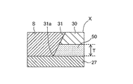
図3に、図1における領域Xを拡大した模式図を示す。領域Xは表面導体層26(導体パッド27)と、はんだバンプSと、接合層50と、ソルダーレジスト層30とが近接する部分である。
本実施形態において接合層50の厚さTは厚さ20〜200nmであることが好ましい。厚さTがこの範囲のときに、表面導体層26(導体パッド27)とソルダーレジスト層30とを強固に接合するという、接合層50の機能を奏するうえで好ましい。
Hereinafter, characteristics of the
FIG. 3 shows a schematic diagram in which the region X in FIG. 1 is enlarged. The region X is a portion where the surface conductor layer 26 (conductor pad 27), the solder bump S, the
In the present embodiment, the thickness T of the
接合層50は銅と窒素とを含む。図4に、実際に作製した、電解めっき銅からなる表面導体層26と接合層50とソルダーレジスト層30とを積層したプリント配線基板1の断面の透過型電子顕微鏡(TEM)による観察像の写真を示す。図4の右下の空隙は、ソルダーレジスト層30の開口31に相当する。表面導体層26の開口31に面する部分には、ニッケルを含む表面処理層を設けている。開口31内にはんだバンプは設けていない。図4においてスケールバーは50nmを示す。X線を照射し生じる光電子エネルギーを測定して元素構成を分析するX線光電子分光法(XPS)を用いて、図4に示す各点における元素組成を評価した。表面導体層26の表面を点eとする。
The
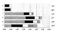
XPSの結果を図5に示す。横軸の数値は各元素の質量比を示す。図5に示す元素以外に炭素が含まれるが、炭素の相対量は他の元素より顕著に多いため図5では示さない。点fから点iまでの各点では窒素(N)及び銅(Cu)が存在する。点iは、電解めっき銅からなる表面導体層26の表面の点eから約115nm離れている。点fに含まれるニッケル(Ni)は、表面導体層26の開口31に面する部分に設けた前記表面処理層に由来するものと考えられる。点j、点kは点eからそれぞれ約145nm、約210nm離れており、これらの点では窒素(N)及び銅(Cu)はほぼ含まれない。電解めっき銅からなる表面導体層26に積層された約120nmの部分(点f、g、h、iを含む)が接合層50に相当し、その上がソルダーレジスト層30に相当する。
The result of XPS is shown in FIG. The numerical value on the horizontal axis indicates the mass ratio of each element. Although carbon is included in addition to the elements shown in FIG. 5, the relative amount of carbon is not shown in FIG. Nitrogen (N) and copper (Cu) exist at each point from point f to point i. The point i is about 115 nm away from the point e on the surface of the
接合層50は、表面導体層26(導体パッド27)とソルダーレジスト層30との界面に介在し、両者を接合する機能を有する。特に、図1及び図3に示すように導体パッド27がSMDパッドである場合に仮に接合層50が存在しないとすれば、開口31へはんだバンプSを導入する際に、導体パッド27(表面導体層26)と、それに乗り上げたソルダーレジスト層30との界面が、開口31の積層基材近傍部分31aを起点に剥離し易いと考えられる。一方、本実施形態によれば、SMDパッドである導体パッド27と、それに乗り上げたソルダーレジスト層30とが接合層50を介して接合されているため、導体パッド27とソルダーレジスト層30との剥離が生じ難い。
The
接合層50は、好ましくは、1つの芳香族環中に窒素を2つ以上有するアゾール化合物と、液状媒体とを含む液状組成物を、電解めっき銅を含む表面導体層26の表面に接触させ、乾燥させることで形成される。前記乾燥を酸化条件、例えば空気雰囲気中で、比較的高温度、例えば20〜130℃、より好ましくは45〜100℃、において行うことが好ましい。この条件での乾燥により、表面導体層26の表面の銅が酸化されて銅(II)イオンとなり、前記アゾール化合物を含む被膜中に拡散すると考えられる。前記アゾール化合物は、窒素原子上の非共有電子対によって銅(II)イオンに配位すると考えられ、1つの銅(II)イオンには複数の窒素原子が配位できると考えられる。しかも、前記アゾール化合物は1つの環に2つ以上の窒素原子を有しており、各窒素原子が銅(II)イオンに配位することができると考えられる。このため、前記アゾール化合物を含む被膜中では、拡散した銅(II)イオンと前記アゾール化合物とが交互に結合して重合体を形成していると考えられる。このような被膜である接合層50は、電解めっき銅を含む表面導体層26と樹脂を含むソルダーレジスト層30との両方に対して親和性を有しており、表面導体層26とソルダーレジスト層30とを接合することができると考えられる。
The
1つの芳香族環中に窒素を2つ以上有するアゾール化合物は、1つの芳香族環中に窒素を2つ以上有するアゾール環を有していればよく環上に置換基を有していてよい。前記アゾール化合物としては、前記アゾール環の部分がジアゾール(1,2−ジアゾール又は1,3−ジアゾール)であるジアゾール化合物、前記アゾール環の部分がトリアゾール(1,2,3−トリアゾール又は1,2,4−トリアゾール)であるトリアゾール化合物、前記アゾール環の部分が1H−テトラゾールであるテトラゾール化合物等が挙げられる。 An azole compound having two or more nitrogen atoms in one aromatic ring may have an azole ring having two or more nitrogen atoms in one aromatic ring, and may have a substituent on the ring. . Examples of the azole compound include a diazole compound in which the azole ring part is diazole (1,2-diazole or 1,3-diazole), and the azole ring part is triazole (1,2,3-triazole or 1,2 , 4-triazole), a tetrazole compound in which the azole ring portion is 1H-tetrazole, and the like.
前記アゾール化合物を含む前記液状組成物の調製に用いる液状媒体としては水又は有機溶媒を用いることができる。
水としてはイオン交換水や蒸留水等の純水が使用できる。
有機溶媒としてはメタノール、エタノール、プロパノール等が挙げられる。
前記液状媒体のうち2種以上の混合物も用いることができる。
As a liquid medium used for the preparation of the liquid composition containing the azole compound, water or an organic solvent can be used.
As the water, pure water such as ion-exchanged water or distilled water can be used.
Examples of the organic solvent include methanol, ethanol, propanol and the like.
A mixture of two or more of the liquid media can also be used.
本実施形態においては、前記液状組成物中における前記アゾール化合物の濃度は、0.001〜10質量%であることが好ましく、0.01〜5質量%であることがより好ましい。前記アゾール化合物の濃度がこの範囲であるとき、表面導体層26とソルダーレジスト層30との接合効果が十分であり、且つ、経済的であると考えられる。
In the present embodiment, the concentration of the azole compound in the liquid composition is preferably 0.001 to 10% by mass, and more preferably 0.01 to 5% by mass. When the concentration of the azole compound is within this range, the bonding effect between the
前記液状組成物を、表面導体層26の表面に接触させる方法としては、特に制限はなく、浸漬、塗布、噴霧等の手段を用いることができる。
前記液状組成物と表面導体層26の表面とを接触させる時間(処理時間)は特に限定されないが、1秒〜10分間とすることができ、5秒〜3分間とすることがより好ましい。処理時間が前記範囲のときに、表面導体層26の表面に十分な厚さの前記液状組成物の被膜を形成することが容易である。前記液状組成物と表面導体層26の表面とを接触させる際の前記液状組成物の温度については5〜50℃とすることが好ましいが、前記の処理時間との関係において適宜設定することができる。
There is no restriction | limiting in particular as a method of making the said liquid composition contact the surface of the
The time (treatment time) for bringing the liquid composition into contact with the surface of the
前記液状組成物と表面導体層26の表面とを接触させた後は、水洗してから乾燥してもよいし、水洗せずに乾燥させてもよい。乾燥温度は既述の通りである。
水洗に使用する水としては、イオン交換水や蒸留水等の純水が好ましいが、水洗の方法や時間には特に制限なく、例えば、浸漬や噴霧等の手段によって適宜の時間洗浄すればよい。
After contacting the liquid composition and the surface of the
The water used for washing is preferably pure water such as ion-exchanged water or distilled water, but the washing method and time are not particularly limited, and may be washed for an appropriate time by means such as immersion or spraying.
前記液状組成物と表面導体層26の表面に接触させる前に、前記表面に、酸洗処理、粗化処理、耐熱処理、防錆処理または化成処理からなる群から選択される少なくとも1つの前処理を行ってもよい。
Before bringing the liquid composition into contact with the surface of the
前記の酸洗処理とは、表面導体層26の表面に付着した油脂成分を除去する為と、銅の表面の酸化皮膜を除去する為に行うものである。この酸洗処理には、塩酸系溶液、硫酸系溶液、硝酸系溶液、硫酸−過酸化水素系溶液、有機酸系溶液、無機酸−有機溶媒系溶液、有機酸−有機溶媒系溶液等の溶液を用いることができる。
The pickling treatment is performed to remove oil and fat components adhering to the surface of the
前記の粗化処理とは、アンカー効果による銅と樹脂の接着性を高めるために行うものであり、銅の表面に凸凹形状が付与され、銅と樹脂材料との密着性を高めることができる。この粗化処理においては、マイクロエッチング法、電解めっき法、無電解めっき法、酸化法(ブラックオキサイド、ブラウンオキサイド)、酸化・還元法、ブラシ研磨法、ジェットスクラブ法等の方法を採用することができる。 The roughening treatment is performed in order to enhance the adhesion between copper and the resin due to the anchor effect. A rough surface is provided on the surface of the copper, and the adhesion between the copper and the resin material can be enhanced. In this roughening treatment, methods such as microetching, electrolytic plating, electroless plating, oxidation (black oxide, brown oxide), oxidation / reduction, brush polishing, jet scrub, etc. may be employed. it can.
前記のマイクロエッチング法においては、例えば、有機酸・第二銅イオン系、硫酸・過酸化水素系、過硫酸塩系、塩化銅系や塩化鉄系の各エッチング剤を使用することができる。
前記の電解めっき法においては、銅の表面に微細な銅粒子を析出させることにより、銅の表面に凸凹を形成させる。
In the microetching method, for example, organic acid / cupric ion type, sulfuric acid / hydrogen peroxide type, persulfate type, copper chloride type or iron chloride type etchants can be used.
In the electrolytic plating method described above, unevenness is formed on the copper surface by precipitating fine copper particles on the copper surface.
前記の耐熱処理は、電解めっき銅を含む表面導体層26の表面に、ニッケル、ニッケル−リン、亜鉛、亜鉛−ニッケル、銅−亜鉛、銅−ニッケル、銅−ニッケル−コバルトまたはニッケル−コバルトから選択される少なくとも1種の被膜を形成する処理である。この被膜の形成は公知の電解めっきによる方法を採用して行うことができるが、電界めっきに限定されるものではなく、蒸着その他の手段を使用しても何ら差し支えない。
The heat-resistant treatment is selected from nickel, nickel-phosphorus, zinc, zinc-nickel, copper-zinc, copper-nickel, copper-nickel-cobalt, or nickel-cobalt on the surface of the
前記の防錆処理とは、電解めっき銅を含む表面導体層26の表面が酸化腐食することを防止するために行うものであり、銅の表面に、亜鉛または亜鉛合金組成のメッキ被膜や、電解クロメートのメッキ被膜を形成する方法を採用することができる。
The rust prevention treatment is performed to prevent the surface of the
前記の化成処理においては、電解めっき銅を含む表面導体層26の表面にスズの不動態被膜を形成する方法や、酸化銅の不動態被膜を形成する方法を採用することができる。
In the chemical conversion treatment, a method of forming a passive film of tin on the surface of the
前記液状組成物を表面導体層26の表面に接触させる前に、銅イオンを含む水溶液を当該表面に接触させてもよい。この銅イオンを含む水溶液は、表面導体層26の表面に形成される接合層50の厚みを均一にさせる機能を有する。銅イオン源としては、水に溶解する銅塩であれば特に限定されず、硫酸銅、硝酸銅、塩化銅、ギ酸銅、酢酸銅等の銅塩を挙げることができる。銅塩を水に可溶化するために、アンモニアや塩酸等を添加してもよい。
Before bringing the liquid composition into contact with the surface of the
前記液状組成物を表面導体層26の表面に接触させた後に、酸性水溶液またはアルカリ性水溶液を前記表面に接触させてもよい。この酸性水溶液またはアルカリ性水溶液も、前記の銅イオンを含む水溶液と同様に、表面導体層26の表面に形成される接合層50の厚みを均一にさせる機能を有する。酸性水溶液またはアルカリ性水溶液は、特に限定されないが、酸性水溶液としては、硫酸、硝酸、塩酸等の鉱酸や、ギ酸、酢酸、乳酸、グリコール酸、アミノ酸等の有機酸を含む水溶液等を挙げることができる。アルカリ性水溶液としては、水酸化ナトリウム、水酸化カリウム等のアルカリ金属の水酸化物や、アンモニア、エタノールアミン、モノプロパノールアミン等のアミン類を含む水溶液を挙げることができる。
After the liquid composition is brought into contact with the surface of the
<プリント配線基板の製造方法>
次に、本実施形態のプリント配線基板1の製造方法の一例を図2A〜Fを参照して説明する。
(1.準備工程(図2A〜2C))
本実施形態では出発材として図2Cに示す積層基材2を用いることができる。積層基材2の詳細は図1を参照して上記で説明した通りである。積層基材2を形成する方法は特に限定されない。
<Method for manufacturing printed wiring board>
Next, an example of the manufacturing method of the printed wiring board 1 of this embodiment is demonstrated with reference to FIG.
(1. Preparation process (FIGS. 2A to 2C))
In this embodiment, the
図2Cに示す積層基材2において、第2導体ビア25及び表面導体層26を形成する方法は特に限定されないが、その一例を図2A及び図2Bを参照して説明する。
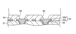
図2Aには、図1に示す本実施形態のプリント配線基板1のうち第2絶縁層24まで完成された中間品の表層近傍を示す。第2絶縁層24にはビアホール(孔部)60が形成されている。前記中間品を形成する方法は特に限定されない。
In the
FIG. 2A shows the vicinity of the surface layer of the intermediate product completed up to the second insulating
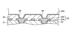
次に、図2Bに示すように、前記中間品において、第2絶縁層24の表面に、ビアホール(孔部)60内に露出した第2電解めっき層23bの表面とともに、無電解めっき又はスパッタリングにより第3シード層26aを形成する。
Next, as shown in FIG. 2B, in the intermediate product, the surface of the second insulating
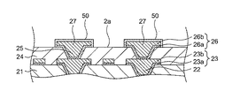
次に、図2Cに示すようにして、第2導体ビア25と第3電解めっき層26bとを形成する。具体的には、図示しないが、第3シード層26aの上にレジストを塗布し、所定のパターンのレジスト層を形成する。続いて、レジスト層で被覆されていない部分に銅による第3電解めっき層26bを形成し、レジスト層の除去、および除去により露出した第3シード層26aをエッチング処理で除去する。これにより、ビアホール60内に第2導体ビア25を形成するとともに、第2絶縁層24の表面に、第3シード層26aと第3電解めっき層26bとからなる表面導体層(第3導体層)26を形成することができる(図2C参照)。
Next, as shown in FIG. 2C, the second conductor via 25 and the third
(2.接合層形成工程(図2D))
次に、図2Dに示すように、表面導体層26の表面に接合層50を形成する。
接合層50の形成方法は既述の通りであり、好ましくは、前記アゾール化合物と、液状媒体とを含む液状組成物を、電解めっき銅を含む表面導体層26の表面に接触させ、乾燥させることで接合層50が形成される。接合層50の形成方法のより具体的な態様は既述の通りである。
(2. Joining layer forming step (FIG. 2D))
Next, as shown in FIG. 2D, the
The method of forming the
(3.ソルダーレジスト前駆層形成工程(図2E))
次に、図2Eに示すように、積層基材2における表面導体層26が形成されている表面2aに、硬化することでソルダーレジスト層30を形成することができる樹脂組成物からなるソルダーレジスト前駆層40を形成するソルダーレジスト前駆層形成工程を行う。
(3. Solder resist precursor layer forming step (FIG. 2E))
Next, as shown to FIG. 2E, the soldering resist precursor which consists of a resin composition which can form the soldering resist
ソルダーレジスト前駆層40は図示するのは単層であるが、複数の層が積層された層であってもよい。
ソルダーレジスト層30を形成することができる樹脂組成物としては、既述の、感光性樹脂と光重合開始剤とを含む感光性樹脂組成物が挙げられる。
The solder resist
Examples of the resin composition that can form the solder resist
ソルダーレジスト前駆層形成工程では、図2Eに示すように、積層基材2の表面2aに前記樹脂組成物からなるソルダーレジスト前駆層40を形成する。このとき、前記樹脂組成物を既述のような溶媒を含む流動体とし、該流動体を積層基材2に塗布させて塗膜を形成し、次いで前記塗膜から前記溶媒を揮発により除去(すなわち乾燥)させることでソルダーレジスト前駆層40を形成することができる。また、ソルダーレジスト前駆層形成工程は、別途ドライフィルムとして調製した、前記樹脂組成物からなるソルダーレジスト前駆層40を積層基材2に積層させる工程であってもよい。
本実施形態において、ソルダーレジスト前駆層40の厚さは特に限定されないが、一般的には10〜70μmである。
In the solder resist precursor layer forming step, as shown in FIG. 2E, a solder resist
In the present embodiment, the thickness of the solder resist
(4.露光工程)
続いて下記の露光工程を行う。露光工程の好ましい実施形態は、ソルダーレジスト前駆層形成工程により形成されたソルダーレジスト前駆層40の、開口31に対応する領域以外の領域に対して光照射して硬化する工程である。露光工程は、典型的には、開口31に対応する領域を選択的に遮蔽する遮光マスクをソルダーレジスト前駆層40の表面に配置した状態で、ソルダーレジスト前駆層40に光照射することで実施可能である。
(4. Exposure process)
Subsequently, the following exposure process is performed. A preferred embodiment of the exposure step is a step in which the region other than the region corresponding to the
露光工程において照射する光の波長、光照度、照射時間等の条件は、ソルダーレジスト前駆層40を構成する樹脂組成物に応じて適宜決定することができる。一般的には照射する光は紫外線である。
Conditions such as the wavelength of light irradiated in the exposure step, light illuminance, and irradiation time can be appropriately determined according to the resin composition constituting the solder resist
(5.現像工程(図2F))
露光工程の後に現像工程を行う。現像工程は、露光工程後に現像液を用いて現像して開口31が形成されたソルダーレジスト層30を形成する工程である(図2F参照)。
(5. Development process (FIG. 2F))
A development process is performed after the exposure process. The development process is a process of forming the solder resist
現像液としては、ソルダーレジスト前駆層40のうち未硬化の部分が可溶であり、且つ、ソルダーレジスト前駆層40のうち光硬化された部分が不溶である溶媒を用いることができる。このような溶媒としては、前記流動体を形成する際に使用したのと同様の溶媒が例示できる。
As the developer, a solvent in which an uncured portion of the solder resist
現像工程で得られたソルダーレジスト層30が、更に光硬化し得るものである場合には、現像工程後に、更に光照射を行い光硬化を完結させる光硬化完結工程が行われることが好ましい。
In the case where the solder resist
また、現像工程で得られたソルダーレジスト層30が熱硬化性樹脂を含むものである場合には、現像工程後に、ソルダーレジスト層30を熱硬化させる熱硬化工程が行われることが好ましい。
Moreover, when the soldering resist
(6.はんだバンプ形成工程)
更に、開口31内の導体パッド27上に、はんだバンプSを設置するはんだバンプ形成工程を行う。本実施形態では更に、はんだバンプSを設置する前に、接合層50のうち、開口31内に露出した部分をエッチングにより除去することが好ましい。本実施形態では更にまた、接合層50の前記部分を除去することで露出した導体パッド27の表面に、酸化を防止するための表面処理層(図示せず)を設けてからはんだバンプ形成工程を行うことが好ましい。表面処理層の具体例は既述の通りである。
(6. Solder bump formation process)
Further, a solder bump forming process is performed in which a solder bump S is placed on the
1:プリント配線基板、2:積層基材、12,23,26:導体層、11,21,24:絶縁層、26:表面導体層、27:導体パッド(SMDパッド)、30:ソルダーレジスト層、31:開口(SMD開口)、50:接合層、S:はんだバンプ 1: printed wiring board, 2: laminated base material, 12, 23, 26: conductor layer, 11, 21, 24: insulating layer, 26: surface conductor layer, 27: conductor pad (SMD pad), 30: solder resist layer , 31: opening (SMD opening), 50: bonding layer, S: solder bump
Claims (2)
前記積層基材は、前記導体層の少なくとも一部として、前記ソルダーレジスト層と接する表面に表面導体層を含む、プリント配線基板であって、
前記表面導体層は電解めっき銅を含み、
前記表面導体層と前記ソルダーレジスト層との間に接合層が介在しており、
前記接合層は、銅と窒素とを含む、厚さ20〜200nmの層である。 A laminated base material including at least one conductor layer and an insulating layer, and a solder resist layer laminated on at least one of the surfaces of the laminated base material,
The laminated substrate is a printed wiring board including a surface conductor layer on a surface in contact with the solder resist layer as at least a part of the conductor layer,
The surface conductor layer includes electroplated copper,
A bonding layer is interposed between the surface conductor layer and the solder resist layer,
The bonding layer is a layer having a thickness of 20 to 200 nm containing copper and nitrogen.
前記表面導体層は、導体パッドを含むパターンを有し、
前記ソルダーレジスト層には開口が設けられており、
前記開口内に前記導体パッドが位置し、
前記導体パッドは、前記ソルダーレジスト層の前記開口の縁辺の下部に食い込むように配置されたSMD(Solder Mask Defined)パッドであり、
前記開口内の前記導体パッド上には、はんだバンプが設けられている。 The printed wiring board according to claim 1,
The surface conductor layer has a pattern including a conductor pad;
An opening is provided in the solder resist layer,
The conductor pad is located in the opening;
The conductor pad is an SMD (Solder Mask Defined) pad arranged so as to bite into the lower part of the edge of the opening of the solder resist layer,
Solder bumps are provided on the conductor pads in the openings.
Priority Applications (1)
| Application Number | Priority Date | Filing Date | Title |
|---|---|---|---|
| JP2016081448A JP2017191893A (en) | 2016-04-14 | 2016-04-14 | Printed wiring board |
Applications Claiming Priority (1)
| Application Number | Priority Date | Filing Date | Title |
|---|---|---|---|
| JP2016081448A JP2017191893A (en) | 2016-04-14 | 2016-04-14 | Printed wiring board |
Publications (1)
| Publication Number | Publication Date |
|---|---|
| JP2017191893A true JP2017191893A (en) | 2017-10-19 |
Family
ID=60086214
Family Applications (1)
| Application Number | Title | Priority Date | Filing Date |
|---|---|---|---|
| JP2016081448A Pending JP2017191893A (en) | 2016-04-14 | 2016-04-14 | Printed wiring board |
Country Status (1)
| Country | Link |
|---|---|
| JP (1) | JP2017191893A (en) |
Cited By (1)
| Publication number | Priority date | Publication date | Assignee | Title |
|---|---|---|---|---|
| CN115558910A (en) * | 2022-11-03 | 2023-01-03 | 重庆海盛鑫铜业有限公司 | Portable tinning machine for copper wire processing and use method |
-
2016
- 2016-04-14 JP JP2016081448A patent/JP2017191893A/en active Pending
Cited By (2)
| Publication number | Priority date | Publication date | Assignee | Title |
|---|---|---|---|---|
| CN115558910A (en) * | 2022-11-03 | 2023-01-03 | 重庆海盛鑫铜业有限公司 | Portable tinning machine for copper wire processing and use method |
| CN115558910B (en) * | 2022-11-03 | 2024-05-07 | 重庆海盛鑫铜业有限公司 | Portable tinning machine for copper wire processing and use method |
Similar Documents
| Publication | Publication Date | Title |
|---|---|---|
| KR101268145B1 (en) | Method for surface treatment of copper and copper | |
| KR101042483B1 (en) | Copper surface treatment method and copper | |
| TW443084B (en) | Multi-layer printed circuit board and its fabricating method, composition material of resin used for filling through hole | |
| CN103733739B (en) | Circuit board | |
| TW200410622A (en) | Multi-layer printed circuit board, its manufacturing method and solder resist composition | |
| JP4973231B2 (en) | Copper etching method and wiring board and semiconductor package using this method | |
| US20100126758A1 (en) | Multilayer printed wiring board and method for manufacturing multilayer printed wiring board | |
| WO2011027884A1 (en) | Substrate for mounting semiconductor chip and method for producing same | |
| KR102105988B1 (en) | Method of forming a metal layer on a photosensitive resin | |
| CN102316668A (en) | Substrate with fine metal pattern, print circuit board and semiconductor device, and production method of substrate with fine metal pattern, print circuit board and semiconductor device | |
| JP2008109087A (en) | Substrate for mounting semiconductor chip, and preprocessing liquid | |
| JP2007109902A (en) | Method for manufacturing multilayer printed wiring board, and photosensitive dry film used for same | |
| JP2004363364A (en) | Metal surface treatment method, multilayer circuit board manufacturing method, semiconductor chip mounting board manufacturing method, semiconductor package manufacturing method, and semiconductor package | |
| JP2013093359A (en) | Semiconductor chip mounting substrate and manufacturing method therefor | |
| CN101772274A (en) | Surface electroplating method of circuit substrate | |
| JP2017191894A (en) | Printed wiring board and manufacturing method of the same | |
| JP5938948B2 (en) | Semiconductor chip mounting substrate and manufacturing method thereof | |
| JP2013089913A (en) | Substrate for mounting semiconductor chip and manufacturing method thereof | |
| JP5691527B2 (en) | Wiring board surface treatment method and wiring board treated by this surface treatment method | |
| JP5682678B2 (en) | Semiconductor chip mounting substrate and manufacturing method thereof | |
| JP2011258597A (en) | Base material with gold plated fine metal pattern, printed wiring board and semiconductor device and manufacturing method thereof | |
| JP7753721B2 (en) | Printed wiring board manufacturing method and semiconductor package manufacturing method | |
| JP2004327803A (en) | Multilayered circuit board, semiconductor chip loading substrate, semiconductor package, and methods of manufacturing them | |
| JP3593351B2 (en) | Method for manufacturing multilayer wiring board | |
| JP2002134655A (en) | Board for semiconductor package, its manufacturing method, the semiconductor package and its manufacturing method |