JP2017198744A - Light control film, method for manufacturing light control film - Google Patents
Light control film, method for manufacturing light control film Download PDFInfo
- Publication number
- JP2017198744A JP2017198744A JP2016087417A JP2016087417A JP2017198744A JP 2017198744 A JP2017198744 A JP 2017198744A JP 2016087417 A JP2016087417 A JP 2016087417A JP 2016087417 A JP2016087417 A JP 2016087417A JP 2017198744 A JP2017198744 A JP 2017198744A
- Authority
- JP
- Japan
- Prior art keywords
- spacer
- liquid crystal
- light control
- control film
- laminate
- Prior art date
- Legal status (The legal status is an assumption and is not a legal conclusion. Google has not performed a legal analysis and makes no representation as to the accuracy of the status listed.)
- Granted
Links
Images



Landscapes
- Liquid Crystal (AREA)
- Laminated Bodies (AREA)
Abstract
Description
本発明は、乗用車の窓等に貼り付けて外来光の透過を制御する調光フィルムに関する。 The present invention relates to a light control film that is attached to a window or the like of a passenger car to control the transmission of extraneous light.
従来、例えば窓に貼り付けて外来光の透過を制御する調光フィルムに関する工夫が種々に提案されている(特許文献1、2)。このような調光フィルムの1つに、液晶を利用したものがある。この液晶を利用した調光フィルムは、透明電極を製造した透明フィルム材により液晶材料を挟持して液晶セルが製造され、この液晶セルを直線偏光板により挟持して作成される。これによりこの調光フィルムでは、液晶に印加する電界の可変により液晶の配向を可変して外来光を遮光したり透過したりし、さらには透過光量を可変したりし、これらにより外来光の透過を制御する。
Conventionally, for example, various devices relating to a light control film that is attached to a window to control the transmission of external light have been proposed (
このような調光フィルムにおける液晶セルの駆動には、液晶表示パネルについて提案されている種々の駆動方法を適用することができる。具体的には、例えばTN(Twisted Nematic)方式、IPS(In−Place−Switching)方式、VA(Virtical Alignment)方式等の駆動方式を適用することができる。 Various driving methods proposed for liquid crystal display panels can be applied to driving the liquid crystal cell in such a light control film. Specifically, for example, a driving method such as a TN (Twisted Nematic) method, an IPS (In-Place-Switching) method, or a VA (Virtual Alignment) method can be applied.
また液晶表示パネルは、マルチドメイン化により視野角特性を向上する工夫が種々に提案されており、特許文献3には、線状突起、点状突起等によるリブを設けて配向層を製造することによるVA方式のマルチドメイン方式(MVA:Multi−domain vertical alignment)が提案されている。
In addition, liquid crystal display panels have been proposed in various ways to improve viewing angle characteristics by using multi-domains. In
ここでVA方式は、液晶の配向を垂直配向と水平配向とで変化させて透過光を制御する方式であり、一般的に、無電界時、液晶を垂直配向させることにより、液晶層を垂直配向層により挟持して液晶セルが構成され、電界の印加により液晶材料を水平配向させるように構成される。ここでマルチドメイン方式とは、電界の可変に対して液晶分子の挙動が異なる領域(ドメイン)を複数設ける方式であり、一般的に、複数領域における光学特性の平均値化(積分化)により視野角特性を向上するために適用される。 Here, the VA method is a method of controlling the transmitted light by changing the alignment of the liquid crystal between vertical alignment and horizontal alignment. Generally, the liquid crystal layer is vertically aligned by vertically aligning the liquid crystal when no electric field is applied. A liquid crystal cell is formed by being sandwiched between layers, and the liquid crystal material is horizontally aligned by application of an electric field. Here, the multi-domain method is a method in which a plurality of regions (domains) in which the behavior of liquid crystal molecules is different with respect to a variable electric field is provided. In general, the field of view is obtained by averaging (integrating) optical characteristics in a plurality of regions. Applied to improve angular characteristics.
ところで調光フィルムは、例えば窓ガラス等に貼り付けて大面積により種々の用途で使用することが予測される。従って簡易な構成により製造できることが望まれる。また窓ガラスに貼り付けて使用する場合、カーテンの機能を担う場合も予測されることにより、充分に入射光を遮光できることが求められる。これらによりVA方式のシングルドメイン方式で駆動することが考えられる。 By the way, it is estimated that a light control film is affixed on a window glass etc., and is used for various uses by a large area. Therefore, it is desired that the product can be manufactured with a simple configuration. Moreover, when pasting on a window glass and using it, it is calculated | required that the function of a curtain is assumed, and it is calculated | required that incident light can fully be shielded. It is conceivable to drive with the single domain method of the VA method.
しかしながらVA方式のシングルドメイン方式では、調光フィルムが黄色味を帯びて視認され、これにより調光フィルムの色味が劣化する問題がある。また中間諧調においては、視野角の変化に係る見る方向の変化によって諧調が変化し、これにより中間諧調において視野角特性の劣化が著しい問題もある。これらの問題を解決することができれば、例えばVA方式によるマルチドメイン方式に適用して、さらにはVA方式以外の方式による調光フィルムに適用して一段と特性を向上することができると考えられる。 However, in the VA single domain system, the light control film is visually recognized as yellowish, and this causes a problem that the color of the light control film deteriorates. Further, in the intermediate gradation, the gradation changes due to the change in the viewing direction according to the change in the viewing angle, and there is a problem that the viewing angle characteristic is significantly deteriorated in the intermediate gradation. If these problems can be solved, it is considered that the characteristics can be further improved by applying to a multi-domain system using the VA system, for example, and further to a light control film using a system other than the VA system.
本発明はこのような状況に鑑みてなされたものであり、例えばVA方式のシングルドメイン方式による調光フィルムにおいて、色味の劣化、中間諧調における視野角特性の劣化を改善する。 The present invention has been made in view of such a situation. For example, in a light-control film by a VA single-domain method, color tone deterioration and deterioration of viewing angle characteristics in intermediate gradation are improved.
本発明者は、上記課題を解決するために鋭意研究を重ね、セルギャップのパターニングにより液晶層の厚みを変化させる、との着想に至り、本発明を完成するに至った。 The present inventor has made extensive studies to solve the above problems, and has come up with the idea that the thickness of the liquid crystal layer is changed by patterning the cell gap, thereby completing the present invention.
具体的には、本発明では、以下のようなものを提供する。 Specifically, the present invention provides the following.
(1) 少なくとも配向層を備えてなる第1及び第2の積層体により液晶層を挟持し、前記第1及び又は第2の積層体に設けられた電極による駆動により前記液晶層の液晶の配向を制御して透過光を制御する調光フィルムにおいて、
前記液晶層の厚み方向における、厚みの差分値が0.1μm以上0.6μm以下である2種類以上のスペーサーの配置によって、前記液晶層において、厚みの異なる第1及び第2の領域が設けられた調光フィルム。
(1) A liquid crystal layer is sandwiched between first and second stacked bodies each having at least an alignment layer, and liquid crystal alignment of the liquid crystal layer is driven by an electrode provided on the first and / or second stacked body. In the light control film that controls transmitted light by controlling
By arranging two or more types of spacers having a thickness difference value of 0.1 μm or more and 0.6 μm or less in the thickness direction of the liquid crystal layer, first and second regions having different thicknesses are provided in the liquid crystal layer. Dimming film.
(1)によれば、厚みの異なる第1及び第2の領域によりセルギャップがパターニングされて液晶層が形成され、液晶層の厚みを変化させることができる。これにより厚みの異なる第1及び第2の領域による光学特性を平均値化して、色味の劣化、中間諧調における視野角特性の劣化を改善することができる。 According to (1), the cell gap is patterned by the first and second regions having different thicknesses to form the liquid crystal layer, and the thickness of the liquid crystal layer can be changed. As a result, the optical characteristics of the first and second regions having different thicknesses can be averaged, and the deterioration of the tint and the viewing angle characteristics in the intermediate gradation can be improved.
(2) (1)において、
前記第1及び第2の領域が、帯状の領域である調光フィルム。
(2) In (1),
The light control film whose said 1st and 2nd area | region is a strip-shaped area | region.
(2)によれば、具体的構成により色味の劣化、中間諧調における視野角特性の劣化を改善することができる。 According to (2), it is possible to improve the deterioration of the tint and the deterioration of the viewing angle characteristics in the intermediate gradation by the specific configuration.
(3) (1)又は(2)において、
前記スペーサーが、ビーズスペーサーである調光フィルム。
(3) In (1) or (2),
A light control film, wherein the spacer is a bead spacer.
(4) (1)又は(2)において、
前記スペーサーが、フォトレジストによる柱形状のスペーサーである調光フィルム。
(4) In (1) or (2),
A light control film, wherein the spacer is a columnar spacer made of a photoresist.
(3)又は(4)によれば、ビーズスペーサーを適用して、又はフォトレジストによるスペーサーを適用して、色味の劣化、中間諧調における視野角特性の劣化を改善することができる。 According to (3) or (4), by applying a bead spacer or applying a spacer by a photoresist, it is possible to improve the deterioration of the color tone and the deterioration of the viewing angle characteristics in intermediate gradation.
(5) (1)又は(2)において
前記スペーサーが、前記第1の積層体に設けられたビーズスペーサーであり、
前記ビーズスペーサーが当接する前記第2の積層体の部位のビッカース硬度値Bが11.8以上35.9以下であり、
前記第1の積層体を平面視した状態で、前記第1の積層体上で前記ビーズスペーサーが占める面積の比率である占有率Aと、前記ビッカース硬度値Bとの乗算値A×Bが、0.42以上である調光フィルム。
(5) In (1) or (2), the spacer is a bead spacer provided in the first laminate,
The Vickers hardness value B of the portion of the second laminate in contact with the bead spacer is 11.8 or more and 35.9 or less,
In a state where the first laminate is viewed in plan, a multiplication value A × B of an occupation ratio A which is a ratio of an area occupied by the bead spacer on the first laminate and the Vickers hardness value B is: The light control film which is 0.42 or more.
(5)によれば、ビッカース硬度値Bが11.8以上35.9以下であることにより、使用中の押圧力等により、対向する面にビーズスペーサーが貫入したりする状況を低減して、セルギャップの不均一化、局所的な配向不良を低減し、さらは液晶材料の漏出を有効に回避することができる。また占有率Aと、ビッカース硬度値Bとの乗算値A×Bが0.42以上であることにより、占有率Aが小さい場合にはビッカース硬度値Bが大きくなるように設定して、ビーズスペーサーへの応力集中に応じた硬度Bによりセルギャップを保持することができ、これにより一段とセルギャップの不均一化、局所的な配向不良を低減し、さらは液晶材料の漏出を有効に回避することができる。これらによりビーズスペーサーに関する信頼性を従来に比して一段と向上することができる。 According to (5), when the Vickers hardness value B is 11.8 or more and 35.9 or less, the situation in which the bead spacer penetrates into the opposing surface due to the pressing force during use, etc. is reduced. It is possible to reduce cell gap nonuniformity and local alignment failure, and to effectively avoid leakage of liquid crystal material. In addition, since the multiplication value A × B of the occupation ratio A and the Vickers hardness value B is 0.42 or more, when the occupation ratio A is small, the Vickers hardness value B is set to be large, and the bead spacer The cell gap can be maintained by the hardness B corresponding to the stress concentration on the substrate, thereby further reducing the cell gap non-uniformity, local alignment failure, and effectively avoiding the leakage of the liquid crystal material. Can do. By these, the reliability regarding a bead spacer can be improved further compared with the past.
(6) 透明フィルム材による第1の基材に少なくとも配向層を製造して第1の積層体を製造する第1の積層体製造工程と、
透明フィルム材による第2の基材に少なくとも配向層を製造して第2の積層体を製造する第2の積層体製造工程と、
前記第1及び第2の積層体により液晶層を挟持してなる液晶セルを製造する積層工程とを備え、
前記第1の積層体製造工程は、
少なくとも第1のスペーサーを配置した第1の領域と、前記液晶層の厚み方向において、前記第1のスペーサーより0.1μm以上0.6μm以下小さい厚みの第2のスペーサーのみを配置した第2の領域とを、前記第1の基材上に形成するスペーサー配置工程を備える調光フィルムの製造方法。
(6) a first laminate manufacturing step of manufacturing a first laminate by manufacturing at least an alignment layer on a first substrate made of a transparent film material;
A second laminate production process for producing a second laminate by producing at least an orientation layer on a second substrate made of a transparent film material;
A lamination process for producing a liquid crystal cell in which a liquid crystal layer is sandwiched between the first and second laminates,
The first laminate manufacturing process includes:
At least a first region in which the first spacer is arranged and a second region in which only the second spacer having a thickness of 0.1 μm or more and 0.6 μm or less smaller than the first spacer is arranged in the thickness direction of the liquid crystal layer. A method of manufacturing a light control film comprising a spacer arrangement step of forming a region on the first base material.
(6)によれば、厚みの異なる第1及び第2の領域によりセルギャップをパターニングし液晶層を形成することができ、液晶層の厚みを変化させることができる。これにより厚みの異なる第1及び第2の領域による光学特性を平均値化して、色味の劣化、中間諧調における視野角特性の劣化を改善することができる。 According to (6), the cell gap can be patterned by the first and second regions having different thicknesses to form the liquid crystal layer, and the thickness of the liquid crystal layer can be changed. As a result, the optical characteristics of the first and second regions having different thicknesses can be averaged, and the deterioration of the tint and the viewing angle characteristics in the intermediate gradation can be improved.
(7) (6)において、
前記第1及び第2のスペーサーがビーズスペーサーであり、
前記スペーサー配置工程は、
前記第1の領域に対応する開口を備えたマスクを前記第1の基材に配置して前記第1のスペーサーを散布して、
前記第1のスペーサーを配置した第1の領域と、前記第2のスペーサーのみを配置した第2の領域とを形成する調光フィルム。
(7) In (6),
The first and second spacers are bead spacers;
The spacer arrangement step includes
A mask having an opening corresponding to the first region is disposed on the first base material, and the first spacer is dispersed.
The light control film which forms the 1st area | region which has arrange | positioned the said 1st spacer, and the 2nd area | region which has arrange | positioned only the said 2nd spacer.
(7)によれば、第1のスペーサーを散布した後に、又は第1のスペーサーを散布する前に、全面に第2のスペーサーを散布したり、第2の領域に対応する開口を備えたマスクを使用して前記第2のスペーサーを散布することにより、第1及び第2の領域を形成することができる。 According to (7), after the first spacer is sprayed or before the first spacer is sprayed, the second spacer is sprayed on the entire surface, or the mask has an opening corresponding to the second region. The first and second regions can be formed by spraying the second spacers using.
本発明によれば、例えばVA方式のシングルドメイン方式による調光フィルムにおいて、色味の劣化、中間諧調における視野角特性の劣化を改善することができる。 ADVANTAGE OF THE INVENTION According to this invention, in the light control film by a VA system single domain system, the deterioration of a color tone and the viewing angle characteristic in intermediate gradation can be improved, for example.
〔第1実施形態〕
〔調光フィルム〕
図1は、本発明の第1実施形態に係る調光フィルムの説明に供する断面図である。この調光フィルム1は、建築物の窓ガラス、ショーケース、屋内の透明パーテーション等の調光を図る部位に、粘着剤層等により貼り付けて使用され、印加電圧の可変により透過光の光量を制御する。
[First Embodiment]
[Light control film]
FIG. 1 is a cross-sectional view for explaining the light control film according to the first embodiment of the present invention. This
調光フィルム1は、液晶を利用して透過光を制御するフィルム材あり、第1及び第2の直線偏光板2、3により調光フィルム用の液晶セル4を挟持して構成される。ここで直線偏光板2、3は、ポリビニルアルコール(PVA)にヨウ素等を含浸させた後、延伸して直線偏光板としての光学的機能を果たす光学機能層が形成され、TAC(トリアセチルセルロース)等の透明フィルム材による基材により光学機能層を挟持して製造される。直線偏光板2、3は、クロスニコル配置により、紫外線硬化性樹脂等による接着剤層により液晶セル4に配置される。なお直線偏光板2、3は、いわゆるE型である塗布型の直線偏光板を適用してもよい。なお直線偏光板3には、液晶セル4側に光学補償に供する位相差フィルム3Aが設けられるものの、位相差フィルム3Aは、必要に応じて省略してもよい。位相差フィルム3Aには、COPフィルム材等による2軸延伸透明フィルム材を適用することができる。
The
液晶セル4は、後述する透明電極への印加電圧により透過光の偏光面を制御する。これにより調光フィルム1は、透過光を制御して種々に調光を図ることができるように構成される。
The
〔液晶セル〕
液晶セル4は、フィルム形状による第1及び第2の積層体である下側積層体5及び上側積層体6により液晶層8を挟持して構成される。下側積層体5は、透明フィルム材による基材10に、透明電極11、配向層12、第1及び第2のスペーサー13A及び13Bを配置して製造される。上側積層体6は、透明フィルム材による基材15に、透明電極16、配向層17を配置して製造される。液晶セル4は、この下側積層体5及び上側積層体6に設けられた透明電極11、16の駆動により、VA方式のシングルドメイン方式により液晶層8に設けられた液晶材料の配向を制御し、これにより透過光の偏光面を制御する。
[Liquid crystal cell]
The
基材10、15は、この種のフィルム材に適用可能な種々の透明フィルム材を適用することができるものの、光学異方性の小さなフィルム材を適用することが望ましい。この実施形態において、基材10、15は、同一の材料、同一の厚みによる透明フィルム材が適用され、より具体的にはポリカーボネートフィルムが適用されるものの、COP(シクロオレフィンポリマー)フィルム等を適用してもよい。
Although various transparent film materials applicable to this kind of film material can be applied to the
透明電極11、16は、この種のフィルム材に適用される各種の電極材料を適用することができ、この実施形態ではITO(Indium Tin Oxide)による透明電極材により形成される。
Various electrode materials applied to this kind of film material can be applied to the
配向層12、17は、光配向層により形成される。ここでこの光配向層に適用可能な光配向材料は、光配向の手法を適用可能な各種の材料を広く適用することができるものの、この実施形態では、例えば光2量化型の材料を使用する。この光2量化型の材料については、「M.Schadt, K.Schmitt, V. Kozinkov and V. Chigrinov : Jpn. J. Appl.Phys., 31, 2155 (1992)」、「M. Schadt, H. Seiberle and A. Schuster : Nature, 381, 212(1996)」等に開示されている。なお配向層12、17は、光配向層に代えて、ポリイミド等の樹脂層を製造し、この樹脂層をラビング処理して製造してもよい。またラビング処理によるライン状微細凹凸形状を賦型処理して配向層を製造してもよい。 The alignment layers 12 and 17 are formed of a photo-alignment layer. Here, as the photo-alignment material applicable to the photo-alignment layer, various materials to which the photo-alignment technique can be applied can be widely applied. However, in this embodiment, for example, a light dimerization type material is used. . The light dimerization type material is described in “M. Schadt, K. Schmitt, V. Kozinkov and V. Chigrinov: Jpn. J. Appl. Phys., 31, 2155 (1992)”, “M. Schadt, H. Seiberle and A. Schuster: Nature, 381, 212 (1996). The alignment layers 12 and 17 may be manufactured by manufacturing a resin layer such as polyimide instead of the photo alignment layer and rubbing the resin layer. Further, the alignment layer may be manufactured by forming a line-shaped fine uneven shape by rubbing.
第1及び第2のスペーサー13A及び13Bは、液晶層8の厚みを規定するために設けられ、この実施形態ではいわゆるビーズスペーサーが適用される。第1及び第2のスペーサー13A及び13Bには、有機材料によるビーズスペーサー、無機材料によるビーズスペーサー等、種々の構成を適用することができる。またこの実施形態において、第1及び第2のスペーサー13A及び13Bは、球形状の構成が適用されるものの、円柱形状、角柱形状等の棒形状(ロッド状)の構成を適用してもよい。
The first and
なお第1及び第2のスペーサー13A及び13Bは、フォトレジストを塗工して露光、現像することにより製造してもよい。なおこの場合、第1及び第2のスペーサー13A及び13Bは、円柱形状、角柱形状等による柱形状、円錐台形状、角錐台形状等により製造される。
The first and
液晶層8は、この種の調光フィルムに適用可能な各種の液晶材料を広く適用することができる。具体的に、液晶層8には、例えば、特開2003−366484号に記載の液晶化合物を用いることができる。また、上市品としては、例えばメルク社製MLC2166等の液晶材料を適用することができる。なお、ゲストホスト方式による場合、液晶層8には、液晶材料と調光に供する色素とが混入されるものの、ゲストホスト方式について提案されている液晶材料と色素との混合物も広く適用することができる。なお液晶セル4は、液晶層8を囲むように、シール材が配置され、このシール材により下側積層体5、上側積層体6が一体に保持され、液晶材料の漏出が防止される。なおシール材は、例えばエポキシ樹脂剤による熱硬化型樹脂、アクリル樹脂剤による紫外線硬化樹脂、熱及び紫外線で硬化する硬化樹脂等が適用される。
Various liquid crystal materials applicable to this type of light control film can be widely applied to the
〔セルギャップのパターニング〕
第1及び第2のスペーサー13A及び13Bは、大きさの異なるセルギャップを製造するためのスペーサーであり、この実施形態では、直径の異なるビーズスペーサーである。調光フィルム1では、この第1及び第2のスペーサー13A及び13Bの配置により、セルギャップをパターニングし、液晶層8の厚みを液晶層8の面内方向で変化させる。これにより調光フィルム1では、液晶層8において、厚みの異なる部位を密接して配置して、この厚みの異なる部位による透過光の色味を平均値化することにより、色味の劣化を防止する。また視野角の変化による諧調の変化についても平均値化し、これにより中間諧調における視野角特性の劣化を防止する。
[Cell gap patterning]
The first and
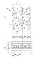
すなわち図2は、セルギャップのパターニングの説明に供する図である。第2のスペーサー13Bは、第1のスペーサー13Aに比して小径である。調光フィルム1は、図2(A)に示すように、この小径である第2のスペーサー13Bのみが配置された第2の領域AR2と、第1のスペーサー13Aが配置された第1の領域AR1とが設けられる。ここでこの実施形態では、第1の領域AR1には、第1のスペーサー13Aと第2のスペーサー13Bとが混在するように設けられるものの、第1のスペーサー13Aのみ設けてもよい。この実施形態において、この第1及び第2の領域AR1、AR2は帯状領域により形成される。
That is, FIG. 2 is a diagram for explaining cell gap patterning. The
このように小径である第2のスペーサー13Bのみが配置された第2の領域AR2と、大径である第1のスペーサー13Aが配置された第1の領域AR1とを設ける場合、調光フィルム1では、厚みが薄く、充分な可撓性を備えた透明フィルム材による基材10、15がスペーサー13A、13Bの大きさで決まるセルギャップにより対向するように保持されることにより、図2(B)に示すように、基材10及び又は15が撓んで、スペーサー13A、13Bに対応するようにセルギャップの大きさが面内方向で変化し、液晶層8の厚みが面内方向で変調されることになる。
Thus, when providing 2nd area | region AR2 in which only the
これにより調光フィルム1では、第1のスペーサー13Aの直径DAにセルギャップが設定された第1の領域AR1と、第2のスペーサー13Bの直径DBにセルギャップが設定された第2の領域AR2とが順次交互に形成される。
Thereby, in the
ここでこの第1及び第2の領域AR1及びAR2が充分に幅狭に製造されている場合、この第1及び第2の領域AR1、AR2の光学特性が平均値化されて知覚され、これにより色味の劣化を防止し、視野角特性の劣化を防止することができる。これに対して第1及び第2の領域AR1及びAR2の幅、繰り返しピッチが大きくなると、第1及び第2の領域AR1、AR2の光学特性を充分に平均値化して知覚させることが困難になる。これにより色味の劣化を充分に防止することが困難になり、また視野角特性の劣化を充分に防止することが困難になる。これにより第1及び第2の領域AR1及びAR2は、充分に幅狭に製造することが望まれるものの、第1及び第2の領域AR1及びAR2の幅、繰り返しピッチPが小さくなると、第1及び第2の領域AR1、AR2において基材10、15を充分に変形させることが難しくなり、これによりセルギャップがばらつき、安定な光学特性を確保できなくなる。
Here, when the first and second regions AR1 and AR2 are manufactured to be sufficiently narrow, the optical characteristics of the first and second regions AR1 and AR2 are averaged and perceived. It is possible to prevent the deterioration of color and the viewing angle characteristics. On the other hand, when the width and the repetition pitch of the first and second regions AR1 and AR2 are increased, it becomes difficult to perceive the optical characteristics of the first and second regions AR1 and AR2 sufficiently averaged. . As a result, it becomes difficult to sufficiently prevent the deterioration of color, and it becomes difficult to sufficiently prevent the deterioration of viewing angle characteristics. As a result, it is desired that the first and second regions AR1 and AR2 be manufactured to be sufficiently narrow, but if the width and the repetition pitch P of the first and second regions AR1 and AR2 are reduced, the first and second regions AR1 and AR2 It becomes difficult to sufficiently deform the
そこで、この実施形態では、第1及び第2の領域AR1及びAR2の繰り返しピッチPが、300μm以上1500μm以下に、好ましくは500μm以上1000μm以下に設定される。またこの繰り返しピッチPの方向に係る第1及び第2の領域AR1、AR2の幅が、150μm以上1000μm以下に、好ましくは250μm以上750μm以下に設定される。 Therefore, in this embodiment, the repetition pitch P of the first and second regions AR1 and AR2 is set to 300 μm to 1500 μm, preferably 500 μm to 1000 μm. The widths of the first and second regions AR1 and AR2 in the direction of the repetitive pitch P are set to 150 μm or more and 1000 μm or less, preferably 250 μm or more and 750 μm or less.
なおこのように透明フィルム材による基材10、15が撓んでスペーサー13A、13Bに対応するようにセルギャップの大きさが面内方向で変化することにより、第1及び第2の領域AR1及びAR2においては、帯状領域により製造して基材10、15の変形を容易とすることができるものの、第1及び第2の領域AR1、AR2は、矩形形状、三角形形状等、種々の形状を適用することができる。
Note that the first and second regions AR1 and AR2 can be obtained by changing the size of the cell gap in the in-plane direction so as to correspond to the
またこのように基材10、15の変形により第1及び第2の領域AR1、AR2をスペーサー13A、13Bに対応する厚みに精度良く設定する観点から、スペーサー13A、13Bは、厚みの差分値が0.1μm以上0.6μm以下、好ましくは厚みの差分値が0.2μm以上0.4μm以下であることが望ましい。このような厚みの範囲に設定することにより、後述する条件を満足するように設定して、ビーズスペーサーに関する信頼性を従来に比して一段と向上することができる。ここでスペーサーの厚みの差分値とは、液晶層8に配置される2種類以上のスペーサーの厚さ方向における高さの差分であり、ビーズスペーサーの場合には、スペーサー13Aと13Bとの球換算の直径(図1中矢印で標記)の差である。これにより、結果として液晶層8の厚みが変化する。
In addition, from the viewpoint of accurately setting the first and second regions AR1 and AR2 to the thicknesses corresponding to the
また第1及び第2の領域AR1及びAR2は、このように帯状領域により形成して、境界及び又は全体を蛇行させるようにしてもよく、これにより規則性を緩和して干渉縞の発生等を防止することができる。またさらに第1及び第2の領域AR1及びAR2は、第1及び第2の領域AR1、AR2の繰り返し方向で、繰り返しピッチP、第1の領域AR1の幅、第2の領域AR2の幅の一部、又は全てを規則的に、又は不規則に変化させてもよい。このように変化させることにより第1及び第2の領域AR1及びAR2の規則性による干渉縞の発生を防止することができる。 In addition, the first and second regions AR1 and AR2 may be formed by band-like regions in this manner, and the boundary and / or the whole may meander, thereby relaxing regularity and generating interference fringes, etc. Can be prevented. Furthermore, the first and second regions AR1 and AR2 are one of the repetition pitch P, the width of the first region AR1, and the width of the second region AR2 in the repetition direction of the first and second regions AR1 and AR2. Parts or all of them may be changed regularly or irregularly. By changing in this way, it is possible to prevent the occurrence of interference fringes due to the regularity of the first and second regions AR1 and AR2.
さらに調光フィルム1では、第1及び第2のスペーサー13A及び13Bがランダムに配置され、これによっても第1及び第2の領域AR1及びAR2を順次交互に設けたことによる規則性を緩和して干渉縞等の発生を防止することができる。
Further, in the
〔シミュレーション結果〕
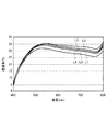
図3は、このように第1及び第2のスペーサー13A、13Bの配置により第1及び第2の領域AR1、AR2を順次交互に設けた場合の確認に供した特性曲線図である。この図3において、符号L1、L2、L3は、直径3.5μm、直径3.7μm、直径3.8μmのスペーサーのみを配置した場合のシミュレーション結果である。これらのシミュレーション結果では、スペーサーの直径を大きくしてセルギャップを大きくした場合、可視光域の長波長側(波長500nm以上)で、徐々に透過率が増大することが判る。
〔simulation result〕
FIG. 3 is a characteristic curve diagram used for confirmation when the first and second regions AR1 and AR2 are alternately provided in this manner by the arrangement of the first and
これに対して符号L4、L5は、この実施形態の調光フィルムのシミュレーション結果である。符号L4は、直径3.7μm、直径3.5μmのスペーサー13A、13Bを使用して(液晶層の厚み方向における、厚みの差分値が0.2μm)、第1及び第2の領域AR1及びAR2の幅を8:2に設定した場合である。符号L5は、直径3.7μm、直径3.5μmのスペーサー13A、13Bを使用して、第1及び第2の領域AR1及びAR2の幅を6:4に設定した場合である。なおこのシミュレーション結果L4、L5では、第1及び第2の領域の繰り返しピッチPは、1000μmである。
On the other hand, symbols L4 and L5 are simulation results of the light control film of this embodiment. Reference numeral L4 indicates that the first and second regions AR1 and AR2 are formed using
符号L4及びL5のシミュレーション結果は、直径3.5μm、直径3.7μmのスペーサーのみを配置した場合のシミュレーション結果L1、L2に対して、シミュレーション結果L1、L2の間の特性であって、第1及び第2の領域AR1及びAR2の幅の比率に応じた特性により透過率を確保することができ、これにより色味の劣化を防止できることが判る。またこのように色味の劣化を防止できることにより、中間諧調における視野角特性の劣化も防止できることが判る。 The simulation results of the symbols L4 and L5 are the characteristics between the simulation results L1 and L2 with respect to the simulation results L1 and L2 when only the spacers having a diameter of 3.5 μm and a diameter of 3.7 μm are arranged. In addition, it can be seen that the transmittance can be ensured by the characteristic according to the ratio of the widths of the second regions AR1 and AR2, thereby preventing the deterioration of the color. Further, it can be seen that the deterioration of the viewing angle characteristic in the intermediate gradation can be prevented by preventing the deterioration of the tint.
〔ビーズスペーサーの詳細構成〕
ここでこの実施形態では、下側積層体5にビーズスペーサー13A及び13Bを配置して調光フィルムを製造するようにして、ビーズスペーサー13A及び13Bが当接する上側積層体6の部位のビッカース硬度値Bが11.8以上35.9以下であるように設定され、ビーズスペーサー13A及び13Bの占有率Aと、ビッカース硬度値Bとの乗算値A×Bが、0.42以上であるように設定される。なおここで占有率Aは、下側積層体5を平面視した状態(鉛直方向から見た状態)で、下側積層体5の面積に対するビーズスペーサー13A及び13Bの面積の占める割合である。これによりこの実施形態では、ビーズスペーサーに関する信頼性を従来に比して一段と向上する。なお、ビッカース硬度の値は、以下の実施例に記載の条件における測定値である。
[Detailed configuration of bead spacer]
Here, in this embodiment, the
すなわちビーズスペーサー13A及び13Bの先端が当接する第2の積層体の部位のビッカース硬度値Bが11.8未満の場合、使用中の押圧力により、ビーズスペーサー13A及び13Bの先端が対向する面に貫入し、その結果、セルギャップが不均一化したり、局所的な配向不良が発生する。また当該部位のビッカース硬度値Bが35.9を超える場合、全体を屈曲した際にクラックが生じる。
That is, when the Vickers hardness value B of the portion of the second laminated body in which the tips of the
またビッカース硬度値Bとの乗算値A×Bが、0.42未満の場合には、ビーズスペーサー13A及び13Bの先端が対向する面に貫入し、その結果、セルギャップが不均一化したり、局所的な配向不良が発生する。
In addition, when the multiplication value A × B with the Vickers hardness value B is less than 0.42, the tips of the
しかしながらビーズスペーサー13A及び13Bが当接する上側積層体6の部位のビッカース硬度値Bが11.8以上35.9以下であり、占有率Aとビッカース硬度値Bとの乗算値A×Bが0.42以上であるように設定すれば、これらの問題を一挙に解決してビーズスペーサーに関する信頼性を従来に比して一段と向上することができる。
However, the Vickers hardness value B of the portion of the
すなわちビーズスペーサー13A及び13Bが当接する上側積層体6の部位のビッカース硬度値Bが11.8以上35.9以下とすれば、使用中の押圧力により、ビーズスペーサー13A及び13Bの先端が対向する面に貫入しないようにし、またクラックの発生を防止することができる。またさらに占有率Aと、ビッカース硬度値Bとの乗算値A×Bが0.42以上であることにより、占有率Aが小さい場合にはビッカース硬度値Bが大きくなるように設定して、ビーズスペーサーへの応力集中に応じた硬度Bによりセルギャップを保持することができ、これにより一段と確実にセルギャップの不均一化、局所的な配向不良を低減し、さらは液晶材料の漏出を有効に回避することができる。これらによりビーズスペーサーに関する信頼性を従来に比して一段と向上することができる。
That is, if the Vickers hardness value B of the
なおこのように、大きさの異なるビーズスペーサー13A及び13Bを配置して液晶層の厚みをパターニングする場合、ビーズスペーサー13A及び13Bの大きさが大きく異なるようになると、上述したビッカース硬度値B、乗算値A×Bの条件を適用できなくなる。しかしながら上述した第1及び第2の領域AR1及びAR2の繰り返しピッチP、第1及び第2の領域AR1、AR2の幅、スペーサー13A、13Bの厚みの差分値に設定する場合にあっては、充分に上述したビッカース硬度値B、乗算値A×Bの条件を適用してビーズスペーサーに関する信頼性を従来に比して一段と向上することができる。
In this way, when the
〔試験結果〕
表1は、このビーズスペーサーに関する構成の確認に供した試験結果を示す図表である。この表1における実施例、比較例は、ビーズスペーサー及びこのビーズスペーサーが当接する配向層に関する構成が異なる点を除いて、同一に構成される。より具体的に、これら実施例、比較例の調光フィルムは、下側積層体5にのみビーズスペーサーを設けるようにし、このビーズスペーサーの大きさの選定、塗布量により占有率Aを可変した。また配向層23Aを製造する際の条件により、ビーズスペーサーの先端が当接する第2の積層体の部位のビッカース硬度値Bを設定した。
〔Test results〕
Table 1 is a chart showing test results used for confirming the configuration of the bead spacer. The examples and comparative examples in Table 1 are configured identically except that the configurations related to the bead spacer and the alignment layer with which the bead spacer abuts are different. More specifically, in the light control films of these Examples and Comparative Examples, a bead spacer was provided only on the
すなわちビーズスペーサーは、ビーズスペーサーを樹脂成分と共に溶剤に分散して製造した塗工液をスピンコートにより塗工した後、乾燥、紫外線照射による硬化、焼成の処理を順次実行することにより、電極22B上にランダムかつ移動困難にビーズスペーサーを配置する。ビーズスペーサーは、この塗工液への投入量、塗工液の塗工膜厚の調整により、占有率を調整する。 In other words, the bead spacer is formed on the electrode 22B by sequentially applying a coating solution prepared by dispersing the bead spacer in a solvent together with a resin component by spin coating, followed by drying, curing by ultraviolet irradiation, and firing. Place the bead spacer randomly and difficult to move. The bead spacer adjusts the occupancy rate by adjusting the amount charged into the coating liquid and the coating film thickness of the coating liquid.
実施例、比較例では、ビーズスペーサーの密度を40個/mm2、50個/mm2、100個/mm2に設定し、またビーズスペーサーには、直径が3μm、6μmによる球形状を適用した。これにより占有率Aを0.028%、0.035%、0.071%、0.113%、0.141%により下側積層体5を製造した。なおビーズスペーサー24は、積水化学社製ミクロパールEXシリーズを適用した。
In Examples and Comparative Examples, the density of bead spacers was set to 40 / mm 2 , 50 / mm 2 , and 100 / mm 2, and spherical shapes with diameters of 3 μm and 6 μm were applied to the bead spacers. . Thus, the
基材21Bは、厚み100μmであり、ハードコート層を備えたCOP(シクロオレフィンポリマー)フィルムである。電極22Bは、厚み20nmにより製造した。 The base material 21B is a COP (cycloolefin polymer) film having a thickness of 100 μm and provided with a hard coat layer. The electrode 22B was manufactured with a thickness of 20 nm.
配向層23Bは、塗工液を乾燥膜厚100nmになるよう塗工し、さらに熱硬化することにより製造した。 The alignment layer 23B was manufactured by coating the coating solution so as to have a dry film thickness of 100 nm and further thermosetting.
これに対してこのビーズスペーサーが当接する面である上側積層体6の配向層23Aは、配向層23Bと同様に、塗工液を塗工して乾燥した後の熱硬化の条件(加熱温度、加熱時間)等の設定によりビッカース硬度値Bを設定した。これにより実施例、比較例では、ビッカース硬度値Bが10.2、11.8、35.9、38.5である上側積層体6を製造した(表3)。なおこの硬度Bは、配向層23Aの作成条件をそれぞれ設定して配向層23Aについて硬さの異なる上側積層体6を製造し、この上側積層体6により調光フィルム1を一旦製造した後、分解して計測した計測値である。またこの計測結果は、12点を計測し、最大値及び最小値を除いて残る10点の平均値による計測結果である。
On the other hand, the alignment layer 23A of the
なおビッカース硬度値Bは、ヘルムートフィッシャー社製PICODENTOR HM500を使用して計測した。計測は、押し込み速度300mN/20sec、リリース速度300mN/20sec、クリープ時間5秒により、最大荷重を100mNの測定条件とした。 The Vickers hardness value B was measured using PICODETOR HM500 manufactured by Helmut Fischer. The measurement was performed under the measurement conditions of a maximum load of 100 mN with an indentation speed of 300 mN / 20 sec, a release speed of 300 mN / 20 sec, and a creep time of 5 seconds.
なお上側積層体の基材21A、電極22Aは、下側積層体13の基材21B、電極22Bと同一に構成した。なお配向層23Aは、硬度Bを調整した点を除いて、配向層23Bと同一に構成した。 The base material 21A and electrode 22A of the upper laminate were configured the same as the base material 21B and electrode 22B of the lower laminate 13. The alignment layer 23A was configured the same as the alignment layer 23B except that the hardness B was adjusted.
表1、表2の各実施例、比較例では、このようにして製造した上側積層体6、下側積層体5により調光フィルムを製造して試験した。表1の試験では、定盤による硬度の高い平滑面に調光フィルムを載置した状態で、1kg/cm2の加重を1分間印加した後、液晶セルを駆動してセルギャップの減少を判断した。またこのように加重した後、上側積層体及び下側積層体を剥離してビーズスペーサーが当接する部位を顕微鏡により観察してビーズスペーサー先端の貫入を観察した。
In each of Examples and Comparative Examples in Tables 1 and 2, a light control film was produced and tested using the
ここでビーズスペーサー13A及び13Bが当接する部位をSEM等の手法を用いて斜視した場合、窪み(凹部)が確認された場合、「フィルム貫入」を「×」判定とし、凹部が認められない場合、「フィルム貫入」を「○」判定とした。
Here, when the part where the
また調光フィルムの状態で、JIS K5600−5−1の曲げ試験の規定に従って、直径2mmの円柱マンドレルに巻き付けてクラックの発生を確認した。この試験で複数サンプルの半数以上で、基材にクラックの発生が確認された場合、「クラック」を「×」により示し、これとは逆に、複数サンプルの半数以上で、基材にクラックの発生が確認されない場合、「クラック」を「○」により示す。 Further, in the state of the light control film, it was wound around a cylindrical mandrel having a diameter of 2 mm in accordance with the bending test of JIS K5600-5-1 to confirm the occurrence of cracks. In this test, when the occurrence of cracks in the substrate is confirmed in more than half of the multiple samples, “crack” is indicated by “x”, and conversely, in more than half of the multiple samples, cracks are generated in the substrate. When the occurrence is not confirmed, “crack” is indicated by “◯”.
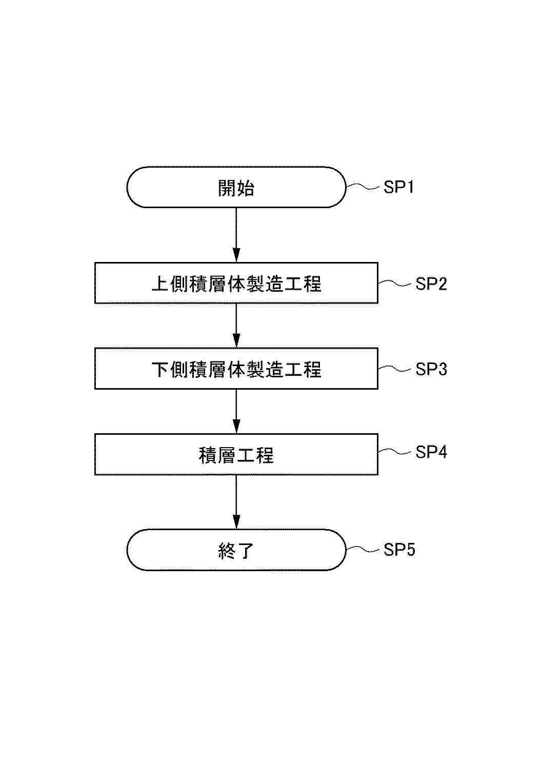
この表1の計測結果では、ビーズスペーサー13A及び13Bが当接する第2の積層体の部位のビッカース硬度値Bが11.8以上35.9以下であり、占有率Aとビッカース硬度値Bとの乗算値A×Bが、0.42以上である場合、フィルム貫入を防止でき、またクラックも発生しないことが確認され、これにより充分にビーズスペーサーに関して信頼性を確保できることが確認された。
In the measurement results of Table 1, the Vickers hardness value B of the second laminate in contact with the
〔製造工程〕
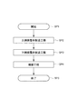
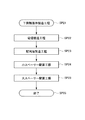
図4は、調光フィルム1の製造工程の説明に供するフローチャートである。この製造工程は、上側積層体製造工程SP2及び下側積層体製造工程SP3において、それぞれ上側積層体6及び下側積層体5が製造される。また積層工程SP4において、液晶層8を間に挟んで、上側積層体6及び下側積層体5を積層した後、シール剤により一体化して調光フィルム1が製造される。
〔Manufacturing process〕
FIG. 4 is a flowchart for explaining the manufacturing process of the
図5は、上側積層体製造工程SP2を詳細に示すフローチャートである。この上側積層体製造工程SP2(SP11)においては、電極製造工程SP12において、透明フィルム材による基材15に、スパッタリング等によりITOによる透明電極16が製造される。また続く配向層製造工程SP13において、配向層17に係る塗工液を塗工して乾燥させ、続いて直線偏光による紫外線の照射により硬化することにより、配向層17を製造する。
FIG. 5 is a flowchart showing the upper laminate manufacturing process SP2 in detail. In the upper laminate manufacturing process SP2 (SP11), in the electrode manufacturing process SP12, the
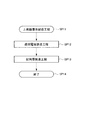
図6は、下側積層体製造工程SP3を詳細に示すフローチャートである。この下側積層体製造工程SP3(SP21)においては、電極製造工程SP22において、透明フィルム材による基材10に、スパッタリングによりITOによる透明電極11が製造される。続いてこの製造工程は、配向層製造工程SP23において、配向層12に係る塗工液を塗工して乾燥、露光することにより、配向層12が形成される。
FIG. 6 is a flowchart showing in detail the lower laminate manufacturing process SP3. In this lower laminate manufacturing process SP3 (SP21), in the electrode manufacturing process SP22, the
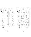
この製造工程では、続く小スペーサー配置工程SP24において、直径の小さい側の第2のスペーサー13Bが配置される。ここでこの実施形態では、配向層12を製造してなる基材10の上空に、第2のスペーサー13Bを分散させた塗工液を噴霧することにより、この塗工液を乾燥させながら第2のスペーサー13Bを基材10に降下させる。ここで第2のスペーサー13Bを分散させた塗工液には接着剤の成分が添加されており、これにより第2のスペーサー13Bは基材10に降下すると、続く紫外線の照射、焼成により、この添加の接着剤成分によって降下位置に第2のスペーサー13Bが保持される。これによりこの製造工程は、図7(A)に示すように、配向層12を製造してなる基材10の全面に、第2のスペーサー13Bをランダムに配置する。
In this manufacturing process, in the subsequent small spacer arrangement step SP24, the
この製造工程では、続く大スペーサー配置工程SP25において、直径の大きい側の第1のスペーサー13Aが配置される。この実施形態では、第1の領域AR1に対応する部位に開口が製造されてなるマスクを、第2のスペーサー13Bをランダムに配置してなる基材10に配置することにより、第1のスペーサー13Bを配置しない部位をマスクする。この状態で、この製造工程は、第2のスペーサー13Aを配置する場合と同様に、マスクした基材10の上空に、第1のスペーサー13Aを分散させた塗工液を噴霧し、この塗工液を乾燥させながら第1のスペーサー13Aを基材10に降下させる。ここで第1のスペーサー13Aを分散させた塗工液にも、接着剤の成分が添加されており、これにより第1のスペーサー13Aは基材10に降下すると、続く硬化、焼成により降下位置に保持される。これによりこの製造工程は、図7(B)に示すように、第1の領域AR1に第1のスペーサー13Aをランダムに配置する。
In this manufacturing process, in the subsequent large spacer arrangement step SP25, the
なお第1及び第2のスペーサー13A、13Bの配置は、種々の手法を適用することができる。
Various methods can be applied to the arrangement of the first and
具体的に大径である第1のスペーサー13Aのみマスクを使用して配置すればよい。すなわち例えば図8(A)に示すように、基材10をマスクした状態で、第1のスペーサー13Aを分散させた塗工液の噴霧により、第1の領域AR1にのみ第1のスペーサー13Aを配置する。続いて図8(B)に示すように、第2のスペーサー13Bを分散させた塗工液の噴霧により、基材10の全面に(第1の領域AR1及び第2の領域AR2に)第2のスペーサー13Bを散布してランダムに配置する。このようにして第1及び第2のスペーサー13A、13Bを配置してもよい。
Specifically, only the
また図9(A)に示すように、基材10をマスクした状態で、第1のスペーサー13Aを分散させた塗工液の噴霧により、第1の領域AR1にのみ第1のスペーサー13Aを配置する。続いて図9(B)に示すように、第2の領域AR2のみ開口を製造したマスクを配置した状態で、第2のスペーサー13Bを分散させた塗工液の噴霧により、第2の領域AR2に第2のスペーサー13Bを散布してランダムに配置する。これにより第1及び第2のスペーサー13A、13Bを配置してもよい。
Further, as shown in FIG. 9A, the
なおこれにより第1の領域AR1は、第1及び第2のスペーサー13A、13Bを混在させるようにしてもよく、径の大きい第1のスペーサー13Aのみ配置するようにしてもよい。
As a result, in the first area AR1, the first and
〔他の実施形態〕
以上、本発明の実施に好適な具体的な構成を詳述したが、本発明は、本発明の趣旨を逸脱しない範囲で、上述の実施形態を組み合わせることができ、さらには上述の実施形態を種々に変更することができる。
[Other Embodiments]
The specific configuration suitable for implementing the present invention has been described in detail above. However, the present invention can be combined with the above-described embodiments without departing from the gist of the present invention, and further, the above-described embodiments can be combined. Various changes can be made.
すなわち上述の実施形態では、ビーズスペーサーを使用する場合について述べたが、本発明はこれに限らず、フォトレジストの露光、現像により柱形状によりスペーサーを製造する場合にも広く適用することができる。 That is, in the above-described embodiment, the case where the bead spacer is used has been described. However, the present invention is not limited to this, and the present invention can be widely applied to the case where the spacer is manufactured in a column shape by exposure and development of a photoresist.
また上述の実施形態では、VA方式によるシングルドメインの調光フィルムに本発明を適用する場合について述べたが、本発明はこれに限らず、VA方式によるマルチドメインの調光フィルムに適用してもよい。このようにすれば、そもそもマルチドメインにより色味の劣化、中間諧調における視野角特性の劣化が改善されている場合に、一段と色味の劣化、中間諧調における視野角特性の劣化を改善することができ、例えば少ないドメイン数によりドメイン数を増大させた場合の光学特性を確保することができる。 In the above-described embodiment, the case where the present invention is applied to a single-domain light control film using the VA method has been described. However, the present invention is not limited thereto, and the present invention may be applied to a multi-domain light control film using the VA method. Good. In this way, when the deterioration of the color tone and the deterioration of the viewing angle characteristic in the intermediate gradation are improved by the multi domain in the first place, the deterioration of the viewing angle characteristic in the intermediate gradation can be further improved. For example, optical characteristics when the number of domains is increased by a small number of domains can be ensured.
また上述の実施形態では、調光を図る部位に、粘着剤層等により調光フィルムを貼り付けて使用する場合について述べたが、本発明はこれに限らず、例えば合わせガラスのように、板ガラス等の透明部材により挟持して積層一体化して使用する場合等にも広く適用することができる。 Further, in the above-described embodiment, the case where the light control film is attached to the part where light control is to be performed by using an adhesive layer or the like has been described, but the present invention is not limited thereto, and for example, a sheet glass such as laminated glass. The present invention can also be widely applied to the case where it is sandwiched by a transparent member such as a laminate and used integrally.
また上述の実施形態では、VA方式によるシングルドメインの調光フィルムに本発明を適用する場合について述べたが、本発明はこれに限らず、VA方式以外のTN方式、IPS方式、FFS方式等によるマルチドメインの調光フィルム、VA方式以外のTN方式、IPS方式、FFS方式等によるシングルドメインの調光フィルムに広く適用することができる。 In the above-described embodiment, the case where the present invention is applied to a single-domain light control film using the VA method has been described. However, the present invention is not limited to this, and the TN method other than the VA method, the IPS method, the FFS method, and the like. The present invention can be widely applied to multi-domain light control films, single-domain light control films by TN methods other than VA methods, IPS methods, FFS methods, and the like.
1 調光フィルム
2、3 直線偏光板
3A 位相差フィルム
4 液晶セル
5 下側積層体(第1の積層体)
6 上側積層体(第2の積層体)
8 液晶層
10、15 基材
11、16 透明電極
12、17 配向層
13A、13B スペーサー
DESCRIPTION OF
6 Upper laminate (second laminate)
8
Claims (7)
前記液晶層の厚み方向における、厚みの差分値が0.1μm以上0.6μm以下である2種類以上のスペーサーの配置によって、前記液晶層において、厚みの異なる第1及び第2の領域が設けられた
調光フィルム。 The liquid crystal layer is sandwiched between the first and second stacked bodies having at least an alignment layer, and the liquid crystal alignment of the liquid crystal layer is controlled by driving with the electrodes provided in the first and second stacked bodies. In the light control film that controls transmitted light,
By arranging two or more types of spacers having a thickness difference value of 0.1 μm or more and 0.6 μm or less in the thickness direction of the liquid crystal layer, first and second regions having different thicknesses are provided in the liquid crystal layer. Light control film.
請求項1に記載の調光フィルム。 The light control film of Claim 1. The said 1st and 2nd area | region is a strip | belt-shaped area | region.
請求項1又は請求項2に記載の調光フィルム。 The light control film according to claim 1, wherein the spacer is a bead spacer.
請求項1又は請求項2に記載の調光フィルム。 The light control film according to claim 1, wherein the spacer is a columnar spacer made of a photoresist.
前記ビーズスペーサーが当接する前記第2の積層体の部位のビッカース硬度値Bが11.8以上35.9以下であり、
前記第1の積層体を平面視した状態で、前記第1の積層体上で前記ビーズスペーサーが占める面積の比率である占有率Aと、前記ビッカース硬度値Bとの乗算値A×Bが、0.42以上である
請求項1又は請求項2に記載の調光フィルム。 The spacer is a bead spacer provided in the first laminate;
The Vickers hardness value B of the portion of the second laminate in contact with the bead spacer is 11.8 or more and 35.9 or less,
In a state where the first laminate is viewed in plan, a multiplication value A × B of an occupation ratio A which is a ratio of an area occupied by the bead spacer on the first laminate and the Vickers hardness value B is: It is 0.42 or more. The light control film of Claim 1 or Claim 2.
透明フィルム材による第2の基材に少なくとも配向層を製造して第2の積層体を製造する第2の積層体製造工程と、
前記第1及び第2の積層体により液晶層を挟持してなる液晶セルを製造する積層工程とを備え、
前記第1の積層体製造工程は、
少なくとも第1のスペーサーを配置した第1の領域と、前記液晶層の厚み方向において、前記第1のスペーサーより0.1μm以上0.6μm以下小さい厚みの第2のスペーサーのみを配置した第2の領域とを、前記第1の基材上に形成するスペーサー配置工程を備える
調光フィルムの製造方法。 A first laminate production process for producing a first laminate by producing at least an orientation layer on a first substrate made of a transparent film material;
A second laminate production process for producing a second laminate by producing at least an orientation layer on a second substrate made of a transparent film material;
A lamination process for producing a liquid crystal cell in which a liquid crystal layer is sandwiched between the first and second laminates,
The first laminate manufacturing process includes:
At least a first region in which the first spacer is arranged and a second region in which only the second spacer having a thickness of 0.1 μm or more and 0.6 μm or less smaller than the first spacer is arranged in the thickness direction of the liquid crystal layer. A method for producing a light control film, comprising a spacer arrangement step of forming a region on the first base material.
前記スペーサー配置工程は、
前記第1の領域に対応する開口を備えたマスクを前記第1の基材に配置して前記第1のスペーサーを散布して、
前記第1のスペーサーを配置した第1の領域と、前記第2のスペーサーのみを配置した第2の領域とを形成する
請求項6に記載の調光フィルムの製造方法。 The first and second spacers are bead spacers;
The spacer arrangement step includes
A mask having an opening corresponding to the first region is disposed on the first base material, and the first spacer is dispersed.
The manufacturing method of the light control film of Claim 6 which forms the 1st area | region which has arrange | positioned the said 1st spacer, and the 2nd area | region which has arrange | positioned only the said 2nd spacer.
Priority Applications (1)
| Application Number | Priority Date | Filing Date | Title |
|---|---|---|---|
| JP2016087417A JP6665661B2 (en) | 2016-04-25 | 2016-04-25 | Light control film, method for manufacturing light control film |
Applications Claiming Priority (1)
| Application Number | Priority Date | Filing Date | Title |
|---|---|---|---|
| JP2016087417A JP6665661B2 (en) | 2016-04-25 | 2016-04-25 | Light control film, method for manufacturing light control film |
Publications (2)
| Publication Number | Publication Date |
|---|---|
| JP2017198744A true JP2017198744A (en) | 2017-11-02 |
| JP6665661B2 JP6665661B2 (en) | 2020-03-13 |
Family
ID=60237835
Family Applications (1)
| Application Number | Title | Priority Date | Filing Date |
|---|---|---|---|
| JP2016087417A Active JP6665661B2 (en) | 2016-04-25 | 2016-04-25 | Light control film, method for manufacturing light control film |
Country Status (1)
| Country | Link |
|---|---|
| JP (1) | JP6665661B2 (en) |
Cited By (4)
| Publication number | Priority date | Publication date | Assignee | Title |
|---|---|---|---|---|
| WO2019142719A1 (en) | 2018-01-17 | 2019-07-25 | 積水化学工業株式会社 | Dimming laminate and resin spacer for dimming laminate |
| JP2019191249A (en) * | 2018-04-19 | 2019-10-31 | 凸版印刷株式会社 | Light control sheet |
| CN112105973A (en) * | 2018-07-02 | 2020-12-18 | 株式会社Lg化学 | Optical modulation element |
| WO2020262219A1 (en) * | 2019-06-28 | 2020-12-30 | 凸版印刷株式会社 | Light-modulating sheet and light-modulating device |
Citations (6)
| Publication number | Priority date | Publication date | Assignee | Title |
|---|---|---|---|---|
| JPS642226U (en) * | 1987-06-23 | 1989-01-09 | ||
| JP2001255539A (en) * | 2000-03-13 | 2001-09-21 | Seiko Epson Corp | Electro-optical device and projection display device |
| JP2004333567A (en) * | 2003-04-30 | 2004-11-25 | Sony Corp | Light control device and imaging device |
| JP2010230759A (en) * | 2009-03-26 | 2010-10-14 | Sekisui Chem Co Ltd | LCD sheet |
| US20120038867A1 (en) * | 2010-08-10 | 2012-02-16 | Samsung Electronics Co., Ltd. | Display substrate, display device including the same, and method of manufacturing the display substrate |
| JP6065143B1 (en) * | 2016-04-25 | 2017-01-25 | 大日本印刷株式会社 | Light control film, laminated glass, and method for manufacturing light control film |
-
2016
- 2016-04-25 JP JP2016087417A patent/JP6665661B2/en active Active
Patent Citations (6)
| Publication number | Priority date | Publication date | Assignee | Title |
|---|---|---|---|---|
| JPS642226U (en) * | 1987-06-23 | 1989-01-09 | ||
| JP2001255539A (en) * | 2000-03-13 | 2001-09-21 | Seiko Epson Corp | Electro-optical device and projection display device |
| JP2004333567A (en) * | 2003-04-30 | 2004-11-25 | Sony Corp | Light control device and imaging device |
| JP2010230759A (en) * | 2009-03-26 | 2010-10-14 | Sekisui Chem Co Ltd | LCD sheet |
| US20120038867A1 (en) * | 2010-08-10 | 2012-02-16 | Samsung Electronics Co., Ltd. | Display substrate, display device including the same, and method of manufacturing the display substrate |
| JP6065143B1 (en) * | 2016-04-25 | 2017-01-25 | 大日本印刷株式会社 | Light control film, laminated glass, and method for manufacturing light control film |
Cited By (18)
| Publication number | Priority date | Publication date | Assignee | Title |
|---|---|---|---|---|
| WO2019142719A1 (en) | 2018-01-17 | 2019-07-25 | 積水化学工業株式会社 | Dimming laminate and resin spacer for dimming laminate |
| KR20200105745A (en) | 2018-01-17 | 2020-09-09 | 세키스이가가쿠 고교가부시키가이샤 | Resin spacer for dimming laminate and dimming laminate |
| US12072583B2 (en) | 2018-01-17 | 2024-08-27 | Sekisui Chemical Co., Ltd. | Dimming laminate and resin spacer for dimming laminate |
| US11644717B2 (en) | 2018-01-17 | 2023-05-09 | Sekisui Chemical Co., Ltd. | Dimming laminate and resin spacer for dimming laminate |
| JP2019191249A (en) * | 2018-04-19 | 2019-10-31 | 凸版印刷株式会社 | Light control sheet |
| JP7206621B2 (en) | 2018-04-19 | 2023-01-18 | 凸版印刷株式会社 | light control sheet |
| US11226519B2 (en) | 2018-07-02 | 2022-01-18 | Lg Chem, Ltd. | Optical modulation element |
| JP2021521491A (en) * | 2018-07-02 | 2021-08-26 | エルジー・ケム・リミテッド | Light modulation element |
| JP7111290B2 (en) | 2018-07-02 | 2022-08-02 | エルジー・ケム・リミテッド | light modulator |
| CN112105973A (en) * | 2018-07-02 | 2020-12-18 | 株式会社Lg化学 | Optical modulation element |
| EP3819686B1 (en) * | 2018-07-02 | 2025-12-03 | Lg Chem, Ltd. | Optical modulation element |
| CN113939765A (en) * | 2019-06-28 | 2022-01-14 | 凸版印刷株式会社 | Dimming sheet and dimming device |
| US20220121054A1 (en) * | 2019-06-28 | 2022-04-21 | Toppan Inc. | Light control sheet and light control device |
| JP2021009188A (en) * | 2019-06-28 | 2021-01-28 | 凸版印刷株式会社 | Light control sheet and light control apparatus |
| WO2020262219A1 (en) * | 2019-06-28 | 2020-12-30 | 凸版印刷株式会社 | Light-modulating sheet and light-modulating device |
| CN113939765B (en) * | 2019-06-28 | 2023-12-12 | 凸版印刷株式会社 | Dimmers and dimming devices |
| JP7434736B2 (en) | 2019-06-28 | 2024-02-21 | Toppanホールディングス株式会社 | Light control sheet and light control device |
| US12078892B2 (en) * | 2019-06-28 | 2024-09-03 | Toppan Inc. | Light control sheet comprising a liquid crystal layer having a liquid crystal composition with a plurality of spacers having a plurality of discrete peaks in a size distribution and light control device |
Also Published As
| Publication number | Publication date |
|---|---|
| JP6665661B2 (en) | 2020-03-13 |
Similar Documents
| Publication | Publication Date | Title |
|---|---|---|
| JP7435667B2 (en) | Light control film and laminated glass | |
| CN109073923B (en) | Light-adjusting film, laminated glass and method for manufacturing light-adjusting film | |
| JP5950014B1 (en) | Light control film | |
| JP2008076950A (en) | Liquid crystal display panel and manufacturing method thereof | |
| JP6665661B2 (en) | Light control film, method for manufacturing light control film | |
| US20230350249A1 (en) | Light control film and laminated glass | |
| JP6065143B1 (en) | Light control film, laminated glass, and method for manufacturing light control film | |
| JP2017194600A (en) | Light control film, laminated glass, and method for manufacturing light control film | |
| JP2018005040A (en) | Light control film and method for forming the light control film | |
| JP6048606B1 (en) | Light control film and method of manufacturing light control film | |
| JP6057012B1 (en) | Light control film | |
| JP6103108B1 (en) | Light control film and method of manufacturing light control film | |
| JP5983852B1 (en) | Light control film and method of manufacturing light control film | |
| JP6183492B1 (en) | Light control film and method of manufacturing light control film | |
| JP2017181826A (en) | Light control film, window | |
| JP2017223809A (en) | Production method of light control film and light control film | |
| JP2017198731A (en) | Lighting control film and manufacturing method of lighting control film | |
| JP2017111422A (en) | Light control film and method for manufacturing light control film | |
| JP2018049232A (en) | Liquid crystal cell | |
| WO2017170578A1 (en) | Light-controlling film and method for manufacturing light-controlling film |
Legal Events
| Date | Code | Title | Description |
|---|---|---|---|
| RD04 | Notification of resignation of power of attorney |
Free format text: JAPANESE INTERMEDIATE CODE: A7424 Effective date: 20160928 |
|
| A621 | Written request for application examination |
Free format text: JAPANESE INTERMEDIATE CODE: A621 Effective date: 20190225 |
|
| A131 | Notification of reasons for refusal |
Free format text: JAPANESE INTERMEDIATE CODE: A131 Effective date: 20191112 |
|
| A521 | Request for written amendment filed |
Free format text: JAPANESE INTERMEDIATE CODE: A523 Effective date: 20200110 |
|
| TRDD | Decision of grant or rejection written | ||
| A01 | Written decision to grant a patent or to grant a registration (utility model) |
Free format text: JAPANESE INTERMEDIATE CODE: A01 Effective date: 20200121 |
|
| A61 | First payment of annual fees (during grant procedure) |
Free format text: JAPANESE INTERMEDIATE CODE: A61 Effective date: 20200203 |
|
| R150 | Certificate of patent or registration of utility model |
Ref document number: 6665661 Country of ref document: JP Free format text: JAPANESE INTERMEDIATE CODE: R150 |