JP2017201300A - 光学モジュールおよび検出方法 - Google Patents
光学モジュールおよび検出方法 Download PDFInfo
- Publication number
- JP2017201300A JP2017201300A JP2017048582A JP2017048582A JP2017201300A JP 2017201300 A JP2017201300 A JP 2017201300A JP 2017048582 A JP2017048582 A JP 2017048582A JP 2017048582 A JP2017048582 A JP 2017048582A JP 2017201300 A JP2017201300 A JP 2017201300A
- Authority
- JP
- Japan
- Prior art keywords
- scintillator
- optical
- refractive index
- output
- optical interface
- Prior art date
- Legal status (The legal status is an assumption and is not a legal conclusion. Google has not performed a legal analysis and makes no representation as to the accuracy of the status listed.)
- Granted
Links
Images





Classifications
-
- G—PHYSICS
- G02—OPTICS
- G02B—OPTICAL ELEMENTS, SYSTEMS OR APPARATUS
- G02B6/00—Light guides; Structural details of arrangements comprising light guides and other optical elements, e.g. couplings
- G02B6/24—Coupling light guides
- G02B6/42—Coupling light guides with opto-electronic elements
- G02B6/4298—Coupling light guides with opto-electronic elements coupling with non-coherent light sources and/or radiation detectors, e.g. lamps, incandescent bulbs, scintillation chambers
-
- G—PHYSICS
- G01—MEASURING; TESTING
- G01T—MEASUREMENT OF NUCLEAR OR X-RADIATION
- G01T1/00—Measuring X-radiation, gamma radiation, corpuscular radiation, or cosmic radiation
- G01T1/02—Dosimeters
- G01T1/10—Luminescent dosimeters
-
- G—PHYSICS
- G02—OPTICS
- G02B—OPTICAL ELEMENTS, SYSTEMS OR APPARATUS
- G02B19/00—Condensers, e.g. light collectors or similar non-imaging optics
- G02B19/0004—Condensers, e.g. light collectors or similar non-imaging optics characterised by the optical means employed
- G02B19/0028—Condensers, e.g. light collectors or similar non-imaging optics characterised by the optical means employed refractive and reflective surfaces, e.g. non-imaging catadioptric systems
-
- G—PHYSICS
- G02—OPTICS
- G02B—OPTICAL ELEMENTS, SYSTEMS OR APPARATUS
- G02B19/00—Condensers, e.g. light collectors or similar non-imaging optics
- G02B19/0033—Condensers, e.g. light collectors or similar non-imaging optics characterised by the use
- G02B19/0076—Condensers, e.g. light collectors or similar non-imaging optics characterised by the use for use with a detector
-
- G—PHYSICS
- G02—OPTICS
- G02B—OPTICAL ELEMENTS, SYSTEMS OR APPARATUS
- G02B27/00—Optical systems or apparatus not provided for by any of the groups G02B1/00 - G02B26/00, G02B30/00
- G02B27/30—Collimators
-
- G—PHYSICS
- G02—OPTICS
- G02B—OPTICAL ELEMENTS, SYSTEMS OR APPARATUS
- G02B6/00—Light guides; Structural details of arrangements comprising light guides and other optical elements, e.g. couplings
- G02B6/24—Coupling light guides
- G02B6/42—Coupling light guides with opto-electronic elements
- G02B6/4201—Packages, e.g. shape, construction, internal or external details
- G02B6/4204—Packages, e.g. shape, construction, internal or external details the coupling comprising intermediate optical elements, e.g. lenses, holograms
- G02B6/4212—Packages, e.g. shape, construction, internal or external details the coupling comprising intermediate optical elements, e.g. lenses, holograms the intermediate optical element being a coupling medium interposed therebetween, e.g. epoxy resin, refractive index matching material, index grease, matching liquid or gel
-
- G—PHYSICS
- G02—OPTICS
- G02B—OPTICAL ELEMENTS, SYSTEMS OR APPARATUS
- G02B6/00—Light guides; Structural details of arrangements comprising light guides and other optical elements, e.g. couplings
- G02B6/24—Coupling light guides
- G02B6/42—Coupling light guides with opto-electronic elements
- G02B6/4201—Packages, e.g. shape, construction, internal or external details
- G02B6/4204—Packages, e.g. shape, construction, internal or external details the coupling comprising intermediate optical elements, e.g. lenses, holograms
- G02B6/4214—Packages, e.g. shape, construction, internal or external details the coupling comprising intermediate optical elements, e.g. lenses, holograms the intermediate optical element having redirecting reflective means, e.g. mirrors, prisms for deflecting the radiation from horizontal to down- or upward direction toward a device
Landscapes
- Physics & Mathematics (AREA)
- General Physics & Mathematics (AREA)
- Optics & Photonics (AREA)
- Health & Medical Sciences (AREA)
- Life Sciences & Earth Sciences (AREA)
- High Energy & Nuclear Physics (AREA)
- Molecular Biology (AREA)
- Spectroscopy & Molecular Physics (AREA)
- Measurement Of Radiation (AREA)
- Optical Couplings Of Light Guides (AREA)
Abstract
Description
a.光学インターフェースが、導光体の少なくとも一部分である。
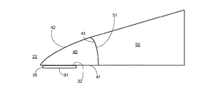
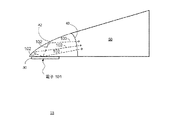
22 光学モジュール
23 光学モジュール
24 光学モジュール
25 光学モジュール
26 光学モジュール
30 シンチレータ
31 別のシンチレータ表面
32 平らな表面
40 光学インターフェース
41 入力表面
42 中間表面
43 出力表面
50 導光体
51 導光体入力界面
60 導光体
61 入力表面
62 中間表面
63 出力表面
70 光学回路
101 電子
102 光線
103 出力光
140 光学インターフェース
150 導光体
240 光学インターフェース
250 導光体
340 光学インターフェース
350 導光体
510 物体
520 システム
531 メモリモジュール
532 コントローラ
533 プロセッサ
540 画像取得モジュール
550 照射モジュール
560 収集および検出モジュール
Claims (15)
- 光学屈折率を有する光学インターフェースであり、入力表面および出力表面を備える光学インターフェースと、
前記光学屈折率に実質的に等しいシンチレータ屈折率を有するシンチレータであり、前記入力表面に光学的に結合された平らな表面を備え、前記シンチレータに荷電粒子が衝突したことに応答して、前記平らな表面を通して放出光を放出するように構成されたシンチレータと
を備え、
前記光学インターフェースが、(i)前記シンチレータからの前記放出光を受け取り、(ii)前記出力表面を通して出力光を出力するように構成されており、
(a)前記光学インターフェースが、導光体の少なくとも一部分であること、
(b)前記入力表面が、光学接触結合によって前記平らな表面に結合されていること、および
(c)前記シンチレータ屈折率に実質的に等しい接着材屈折率を有する接着材によって、前記入力表面が前記平らな表面に取り付けられていること
のうち少なくとも1つが真である光学モジュール。 - 前記出力光が、前記出力表面の領域を通って、前記出力表面の前記領域に対して70度から110度の間の範囲の角度で射出する、請求項1に記載の光学モジュール。
- 前記平らな表面が前記入力表面と接触した、請求項1に記載の光学モジュール。
- 前記光学インターフェースが、前記出力表面に向かう前記放出光を平行にするように構成された放物面鏡を備える、請求項1に記載の光学モジュール。
- 前記出力表面が、3次元球面のセグメントとして形作られた、請求項1に記載の光学モジュール。
- 前記出力表面が直線的形状を有する、請求項1に記載の光学モジュール。
- 前記出力表面が非直線的形状を有する、請求項1に記載の光学モジュール。
- 前記光学インターフェース屈折率が前記シンチレータ屈折率に等しい、請求項1から7のいずれか1項に記載の光学モジュール。
- 前記光学インターフェース屈折率が、前記シンチレータ屈折率と最大10パーセント異なる、請求項1から7のいずれか1項に記載の光学モジュール。
- 前記入力表面が、前記出力表面に関して配向された、請求項1から7のいずれか1項に記載の光学モジュール。
- 前記光学インターフェースおよび前記シンチレータがサファイアでできている、請求項1から7のいずれか1項に記載の光学モジュール。
- シンチレータ屈折率を有するシンチレータの平らな表面を通して放出光を放出するステップであり、前記放出光の前記放出が、前記シンチレータに荷電粒子が衝突したことに対する応答であるステップと、
光学屈折率を有する光学インターフェースの入力表面を通して前記放出光を受け取るステップと、
前記光学インターフェースの出力表面を通して、出力光を、前記出力表面の領域を通して、前記出力表面の前記領域に対して70度から110度の間の範囲の角度で出力するステップと
を含み、
前記光学屈折率が前記シンチレータ屈折率に等しく、または前記シンチレータ屈折率と10パーセント以下だけ異なり、
(a)前記光学インターフェースが、導光体の少なくとも一部分であること、および
(b)前記光学インターフェースの前記出力表面が、前記導光体の一部分と直接に接触していること
のうち少なくとも1つが真である検出方法。 - 前記光学インターフェースが、前記出力表面に向かう前記放出光を平行にするように構成された放物面鏡を備える、請求項12に記載の方法。
- 前記出力光が、前記出力表面の領域を通って、前記出力表面の前記領域に対して70度から110度の間の範囲の角度で射出する、請求項12または13に記載の方法。
- 前記平らな表面が前記入力表面と接触した、請求項12または13に記載の方法。
Applications Claiming Priority (2)
| Application Number | Priority Date | Filing Date | Title |
|---|---|---|---|
| US15/069,496 US9759883B1 (en) | 2016-03-14 | 2016-03-14 | Optical module and a detection method |
| US15/069,496 | 2016-03-14 |
Publications (2)
| Publication Number | Publication Date |
|---|---|
| JP2017201300A true JP2017201300A (ja) | 2017-11-09 |
| JP7053155B2 JP7053155B2 (ja) | 2022-04-12 |
Family
ID=59758611
Family Applications (1)
| Application Number | Title | Priority Date | Filing Date |
|---|---|---|---|
| JP2017048582A Active JP7053155B2 (ja) | 2016-03-14 | 2017-03-14 | 光学モジュールおよび検出方法 |
Country Status (2)
| Country | Link |
|---|---|
| US (1) | US9759883B1 (ja) |
| JP (1) | JP7053155B2 (ja) |
Families Citing this family (1)
| Publication number | Priority date | Publication date | Assignee | Title |
|---|---|---|---|---|
| JP6739207B2 (ja) * | 2016-03-31 | 2020-08-12 | 株式会社日立ハイテク | 荷電粒子線装置 |
Citations (10)
| Publication number | Priority date | Publication date | Assignee | Title |
|---|---|---|---|---|
| JPS5529397A (en) * | 1978-08-24 | 1980-03-01 | Micro Mega Sa | Dental hand piece |
| JPS5529397B1 (ja) * | 1971-02-01 | 1980-08-02 | ||
| US4560882A (en) * | 1984-08-31 | 1985-12-24 | Regents Of The University Of California | High-efficiency X-radiation converters |
| JP2002214349A (ja) * | 2000-11-27 | 2002-07-31 | Koninkl Philips Electronics Nv | X線検出モジュール |
| US6750456B1 (en) * | 2000-05-23 | 2004-06-15 | Southeastern Universities Research Assn., Inc. | Optical coupler |
| JP2011107122A (ja) * | 2009-11-19 | 2011-06-02 | Toshiba Corp | 可変なライトガイド厚を有するガンマ線検出モジュール |
| JP2012037417A (ja) * | 2010-08-09 | 2012-02-23 | Toshiba Corp | 核医学イメージング装置及び解析システム |
| JP2012159360A (ja) * | 2011-01-31 | 2012-08-23 | Toshiba Corp | シンチレーション検出器 |
| JP2012533734A (ja) * | 2009-07-16 | 2012-12-27 | ユニバーシテット ヤギエロンスキ | ガンマ量子反応の位置及び時間を測定するストリップ装置と方法及び陽電子放射断層撮影においてガンマ量子反応の位置及び時間を測定するストリップ装置の使用方法 |
| WO2014128957A1 (ja) * | 2013-02-25 | 2014-08-28 | 株式会社日立製作所 | シンチレータ及び放射線検出器 |
Family Cites Families (2)
| Publication number | Priority date | Publication date | Assignee | Title |
|---|---|---|---|---|
| US7738088B2 (en) * | 2007-10-23 | 2010-06-15 | Gii Acquisition, Llc | Optical method and system for generating calibration data for use in calibrating a part inspection system |
| US8829451B2 (en) * | 2012-06-13 | 2014-09-09 | Hermes Microvision, Inc. | High efficiency scintillator detector for charged particle detection |
-
2016
- 2016-03-14 US US15/069,496 patent/US9759883B1/en active Active
-
2017
- 2017-03-14 JP JP2017048582A patent/JP7053155B2/ja active Active
Patent Citations (10)
| Publication number | Priority date | Publication date | Assignee | Title |
|---|---|---|---|---|
| JPS5529397B1 (ja) * | 1971-02-01 | 1980-08-02 | ||
| JPS5529397A (en) * | 1978-08-24 | 1980-03-01 | Micro Mega Sa | Dental hand piece |
| US4560882A (en) * | 1984-08-31 | 1985-12-24 | Regents Of The University Of California | High-efficiency X-radiation converters |
| US6750456B1 (en) * | 2000-05-23 | 2004-06-15 | Southeastern Universities Research Assn., Inc. | Optical coupler |
| JP2002214349A (ja) * | 2000-11-27 | 2002-07-31 | Koninkl Philips Electronics Nv | X線検出モジュール |
| JP2012533734A (ja) * | 2009-07-16 | 2012-12-27 | ユニバーシテット ヤギエロンスキ | ガンマ量子反応の位置及び時間を測定するストリップ装置と方法及び陽電子放射断層撮影においてガンマ量子反応の位置及び時間を測定するストリップ装置の使用方法 |
| JP2011107122A (ja) * | 2009-11-19 | 2011-06-02 | Toshiba Corp | 可変なライトガイド厚を有するガンマ線検出モジュール |
| JP2012037417A (ja) * | 2010-08-09 | 2012-02-23 | Toshiba Corp | 核医学イメージング装置及び解析システム |
| JP2012159360A (ja) * | 2011-01-31 | 2012-08-23 | Toshiba Corp | シンチレーション検出器 |
| WO2014128957A1 (ja) * | 2013-02-25 | 2014-08-28 | 株式会社日立製作所 | シンチレータ及び放射線検出器 |
Also Published As
| Publication number | Publication date |
|---|---|
| US9759883B1 (en) | 2017-09-12 |
| US20170261713A1 (en) | 2017-09-14 |
| JP7053155B2 (ja) | 2022-04-12 |
Similar Documents
| Publication | Publication Date | Title |
|---|---|---|
| TWI603364B (zh) | 使用電子束系統來檢查關注區域 | |
| JP6191957B2 (ja) | コンプトンカメラ | |
| US7659514B2 (en) | Asymmetric annular detector | |
| JP7053155B2 (ja) | 光学モジュールおよび検出方法 | |
| CN103325708A (zh) | 晶圆缺陷横切观测装置 | |
| Sinitsyna et al. | Supernova remnants: The Crab Nebula, Cassiopeia A, and Tycho as sources of cosmic rays in our galaxy | |
| Austin et al. | Development of a hard x-ray imaging polarimeter | |
| TW201344736A (zh) | 具有延伸動態範圍之光倍增管 | |
| Weekes | The atmospheric Cherenkov imaging technique for very high energy gamma-ray astronomy | |
| Kerrick et al. | Search for TeV Gamma-Ray Emission from AGN's | |
| JP7140902B2 (ja) | 荷電粒子線装置 | |
| Barres de Almeida | Status of the Cherenkov telescope array project | |
| Ward et al. | Light-Trap: a SiPM upgrade for VHE astronomy and beyond | |
| Meyer | The opacity of the universe for high and very high energy {gamma}-rays | |
| CN116594051B (zh) | 一种大面积高空间和时间分辨超硬x射线成像系统 | |
| CN108693550B (zh) | 一种基于光学性能调制的电离辐射检测方法及系统 | |
| CN116300293B (zh) | 基于单束激光的双时刻x射线背光照相系统及方法 | |
| Miyasaka et al. | Development of a small-scale prototype of Fresnel optics for cosmic ray observation | |
| Tsujimoto et al. | Multiwavelength observations of the blazar BL Lacertae in June 2015 | |
| Bloom et al. | Toward a Next Generation High-Energy Gamma-Ray Telescope | |
| Arefiev et al. | Hard x-ray concentrator experiment for Spectrum-X-Gamma mission | |
| Bloom et al. | The Gamma-Ray large Area Space Telescope Mission | |
| CN119916431A (zh) | 一种基于氮化硼薄膜闪烁屏的微米级超高分辨飞行时间中子成像探测器及其制造方法 | |
| Frogget et al. | Atlas Axial Radiography | |
| KR100630575B1 (ko) | 전자기파 영상기기용 오목형 섬광체 |
Legal Events
| Date | Code | Title | Description |
|---|---|---|---|
| A621 | Written request for application examination |
Free format text: JAPANESE INTERMEDIATE CODE: A621 Effective date: 20200305 |
|
| A131 | Notification of reasons for refusal |
Free format text: JAPANESE INTERMEDIATE CODE: A131 Effective date: 20201217 |
|
| A521 | Request for written amendment filed |
Free format text: JAPANESE INTERMEDIATE CODE: A523 Effective date: 20210316 |
|
| A131 | Notification of reasons for refusal |
Free format text: JAPANESE INTERMEDIATE CODE: A131 Effective date: 20210804 |
|
| A521 | Request for written amendment filed |
Free format text: JAPANESE INTERMEDIATE CODE: A523 Effective date: 20211028 |
|
| TRDD | Decision of grant or rejection written | ||
| A01 | Written decision to grant a patent or to grant a registration (utility model) |
Free format text: JAPANESE INTERMEDIATE CODE: A01 Effective date: 20220307 |
|
| A61 | First payment of annual fees (during grant procedure) |
Free format text: JAPANESE INTERMEDIATE CODE: A61 Effective date: 20220331 |
|
| R150 | Certificate of patent or registration of utility model |
Ref document number: 7053155 Country of ref document: JP Free format text: JAPANESE INTERMEDIATE CODE: R150 |
|
| R250 | Receipt of annual fees |
Free format text: JAPANESE INTERMEDIATE CODE: R250 |