JP2017201726A - Semiconductor device and manufacturing method of the same - Google Patents
Semiconductor device and manufacturing method of the same Download PDFInfo
- Publication number
- JP2017201726A JP2017201726A JP2017157093A JP2017157093A JP2017201726A JP 2017201726 A JP2017201726 A JP 2017201726A JP 2017157093 A JP2017157093 A JP 2017157093A JP 2017157093 A JP2017157093 A JP 2017157093A JP 2017201726 A JP2017201726 A JP 2017201726A
- Authority
- JP
- Japan
- Prior art keywords
- circuit pattern
- semiconductor device
- ceramic substrate
- sealing resin
- circuit
- Prior art date
- Legal status (The legal status is an assumption and is not a legal conclusion. Google has not performed a legal analysis and makes no representation as to the accuracy of the status listed.)
- Pending
Links
Images


Classifications
-
- H—ELECTRICITY
- H10—SEMICONDUCTOR DEVICES; ELECTRIC SOLID-STATE DEVICES NOT OTHERWISE PROVIDED FOR
- H10W—GENERIC PACKAGES, INTERCONNECTIONS, CONNECTORS OR OTHER CONSTRUCTIONAL DETAILS OF DEVICES COVERED BY CLASS H10
- H10W72/00—Interconnections or connectors in packages
- H10W72/50—Bond wires
- H10W72/541—Dispositions of bond wires
- H10W72/5445—Dispositions of bond wires being orthogonal to a side surface of the chip, e.g. parallel arrangements
-
- H—ELECTRICITY
- H10—SEMICONDUCTOR DEVICES; ELECTRIC SOLID-STATE DEVICES NOT OTHERWISE PROVIDED FOR
- H10W—GENERIC PACKAGES, INTERCONNECTIONS, CONNECTORS OR OTHER CONSTRUCTIONAL DETAILS OF DEVICES COVERED BY CLASS H10
- H10W72/00—Interconnections or connectors in packages
- H10W72/851—Dispositions of multiple connectors or interconnections
- H10W72/874—On different surfaces
- H10W72/884—Die-attach connectors and bond wires
-
- H—ELECTRICITY
- H10—SEMICONDUCTOR DEVICES; ELECTRIC SOLID-STATE DEVICES NOT OTHERWISE PROVIDED FOR
- H10W—GENERIC PACKAGES, INTERCONNECTIONS, CONNECTORS OR OTHER CONSTRUCTIONAL DETAILS OF DEVICES COVERED BY CLASS H10
- H10W74/00—Encapsulations, e.g. protective coatings
-
- H—ELECTRICITY
- H10—SEMICONDUCTOR DEVICES; ELECTRIC SOLID-STATE DEVICES NOT OTHERWISE PROVIDED FOR
- H10W—GENERIC PACKAGES, INTERCONNECTIONS, CONNECTORS OR OTHER CONSTRUCTIONAL DETAILS OF DEVICES COVERED BY CLASS H10
- H10W90/00—Package configurations
- H10W90/701—Package configurations characterised by the relative positions of pads or connectors relative to package parts
- H10W90/751—Package configurations characterised by the relative positions of pads or connectors relative to package parts of bond wires
- H10W90/754—Package configurations characterised by the relative positions of pads or connectors relative to package parts of bond wires between a chip and a stacked insulating package substrate, interposer or RDL
Landscapes
- Structures Or Materials For Encapsulating Or Coating Semiconductor Devices Or Solid State Devices (AREA)
Abstract
【課題】本発明は半導体装置の小型化と信頼性の向上を低コストで両立させた半導体装置およびその製造方法の提供を目的とする。【解決手段】本発明に係る半導体装置は、セラミック基板1と、セラミック基板1表面に配置された複数の回路パターン1aと、少なくとも1つの回路パターン1aの表面に配置された半導体素子2と、セラミック基板1、複数の回路パターン1aおよび半導体素子2を封止する封止樹脂4と、を備え、隣接する回路パターン1aの対向する側面にはアンダーカット部1aaが形成され、アンダーカット部1aaにおいて、回路パターン1aのセラミック基板1に接する面の端部12よりも、回路パターン1aの表面の端部11の方が当該回路パターン1aの外側に突出しており、アンダーカット部1aaにも封止樹脂4が充填されることを特徴とする。【選択図】図1An object of the present invention is to provide a semiconductor device and a method for manufacturing the semiconductor device, in which miniaturization and improvement in reliability of the semiconductor device are compatible at low cost. A semiconductor device according to the present invention includes a ceramic substrate 1, a plurality of circuit patterns 1a arranged on the surface of the ceramic substrate 1, a semiconductor element 2 arranged on the surface of at least one circuit pattern 1a, and a ceramic. A substrate 1, a plurality of circuit patterns 1 a and a sealing resin 4 for sealing the semiconductor element 2. Undercut portions 1 aa are formed on opposite side surfaces of adjacent circuit patterns 1 a, The end 11 of the surface of the circuit pattern 1a protrudes to the outside of the circuit pattern 1a rather than the end 12 of the surface of the circuit pattern 1a that contacts the ceramic substrate 1. Is filled. [Selection] Figure 1
Description
本発明は半導体装置およびその製造方法に関し、例えば、電気自動車や電車等のモータを制御するインバータや回生用のコンバータに使用される半導体装置およびその製造方法に関する。 The present invention relates to a semiconductor device and a manufacturing method thereof, for example, a semiconductor device used for an inverter for controlling a motor of an electric vehicle, a train or the like, or a converter for regeneration, and a manufacturing method thereof.
従来の半導体装置は、セラミック基板、セラミック基板上に配置された回路パターン、回路パターンに実装された半導体素子、回路パターン間および回路パターンと半導体素子とを接続するボンディングワイヤなどから構成される。半導体装置において、回路パターン間を絶縁するために、セラミック基板が剥き出しとなる絶縁部が設けられていた。セラミック基板のサイズは、回路パターンの面積および絶縁部の幅に依存していた。 A conventional semiconductor device includes a ceramic substrate, a circuit pattern disposed on the ceramic substrate, a semiconductor element mounted on the circuit pattern, a bonding wire connecting the circuit pattern and the semiconductor element, and the like. In a semiconductor device, in order to insulate between circuit patterns, an insulating portion from which a ceramic substrate is exposed is provided. The size of the ceramic substrate depends on the area of the circuit pattern and the width of the insulating portion.
セラミック基板、回路パターン、半導体素子およびボンディングワイヤは、例えばエポキシ樹脂により封止される。セラミック基板および回路パターンと、エポキシ樹脂との密着性が悪いため、セラミック基板にポリイミド系、またはポリアミドイミド系の低ヤング率の樹脂を予め塗布してから樹脂封止を行うことで、エポキシ樹脂の剥離を防止していた(例えば、特許文献1参照)。 The ceramic substrate, circuit pattern, semiconductor element, and bonding wire are sealed with, for example, an epoxy resin. Since the adhesion between the ceramic substrate and the circuit pattern and the epoxy resin is poor, by applying a resin based on a low Young's modulus such as a polyimide or polyamideimide to the ceramic substrate in advance, The peeling was prevented (for example, refer patent document 1).
従来の半導体装置は以上のように構成されているので、セラミック基板を小型化するためには、回路パターンの面積を減らすか、絶縁部の幅を狭める必要があり、組立性の低下および絶縁性の低下の問題があった。 Since the conventional semiconductor device is configured as described above, in order to reduce the size of the ceramic substrate, it is necessary to reduce the area of the circuit pattern or reduce the width of the insulating portion. There was a problem of lowering.
また、エポキシ樹脂の剥離を抑制するには、上述の低ヤング率の樹脂を塗布することが必要であり、塗布のための製造工程が増大するため、製造コストが増大する問題があった。製造コストを削減するために、低ヤング率の樹脂を塗布しなければ、エポキシ樹脂の密着性が悪化することにより剥離が発生する。エポキシ樹脂の剥離により、エポキシ樹脂で保持している構造物(例えばアルミワイヤや端子)の接合寿命低下、また、セラミック基板上の回路パターン間の絶縁性の低下などが生じる問題があった。 Moreover, in order to suppress the peeling of the epoxy resin, it is necessary to apply the above-mentioned resin having a low Young's modulus, and there is a problem that the manufacturing cost increases because the manufacturing process for coating increases. If a low Young's modulus resin is not applied in order to reduce the manufacturing cost, the adhesiveness of the epoxy resin deteriorates and peeling occurs. Due to the peeling of the epoxy resin, there is a problem that the bonding life of the structure (eg, aluminum wire or terminal) held by the epoxy resin is reduced and the insulation between the circuit patterns on the ceramic substrate is reduced.
この発明は以上のような課題を解決するためになされたものであり、半導体装置の小型化と信頼性の向上を低コストで両立させた半導体装置およびその製造方法の提供を目的とする。 The present invention has been made to solve the above-described problems, and an object of the present invention is to provide a semiconductor device and a method for manufacturing the same, which can reduce the size and improve the reliability of the semiconductor device at a low cost.
本発明に係る半導体装置は、セラミック基板と、セラミック基板表面に配置された複数の回路パターンと、少なくとも1つの回路パターンの表面に配置された半導体素子と、セラミック基板、複数の回路パターンおよび半導体素子を封止する封止樹脂と、を備え、隣接する回路パターンの対向する側面にはアンダーカット部が形成され、アンダーカット部において、回路パターンのセラミック基板に接する面の端部よりも、回路パターンの表面の端部の方が回路パターンの外側に突出しており、かつ、回路パターンのセラミック基板に接する面と回路パターンの表面との間に凹部が設けられ、アンダーカット部にも封止樹脂が充填されることを特徴とする。 A semiconductor device according to the present invention includes a ceramic substrate, a plurality of circuit patterns disposed on the surface of the ceramic substrate, a semiconductor element disposed on the surface of at least one circuit pattern, the ceramic substrate, the plurality of circuit patterns, and the semiconductor element. And an undercut portion is formed on the opposite side surface of the adjacent circuit pattern, and the circuit pattern is located at the undercut portion rather than the end of the surface contacting the ceramic substrate of the circuit pattern. The edge of the surface of the circuit pattern protrudes to the outside of the circuit pattern, and a recess is provided between the surface of the circuit pattern that contacts the ceramic substrate and the surface of the circuit pattern. It is filled.
隣接する回路パターンの対向する側面にアンダーカット部を設けることにより、回路パターンの表面の面積を縮小することなく、回路パターンの底面の面積を縮小することが可能である。よって、回路パターン表面の機能的に必要な面積を確保し、かつ、絶縁に必要な回路パターン間の間隔を確保することができる。つまり、絶縁性を低下させることなく、回路パターン間の間隔をより狭くすることが可能なため、回路パターンが形成されるセラミック基板の面積を縮小することが可能となり、半導体装置の小型化が可能である。 By providing the undercut portions on the opposite side surfaces of the adjacent circuit patterns, it is possible to reduce the area of the bottom surface of the circuit pattern without reducing the area of the surface of the circuit pattern. Therefore, a functionally necessary area on the surface of the circuit pattern can be secured, and an interval between circuit patterns necessary for insulation can be secured. In other words, the distance between circuit patterns can be made narrower without degrading insulation, so the area of the ceramic substrate on which the circuit patterns are formed can be reduced, and the semiconductor device can be downsized. It is.
また、回路パターンの側面にアンダーカット部を設けることにより、アンダーカット部にも封止樹脂が充填され、セラミック基板と封止樹脂の密着性が向上するため、封止樹脂の剥離が抑制され、半導体装置の信頼性が向上する。つまり、アンダーカット部を設けることにより、絶縁性の向上による半導体装置の小型化と、剥離の抑制による信頼性の向上の2つの効果を同時に得ることが可能である。 In addition, by providing an undercut portion on the side surface of the circuit pattern, the undercut portion is filled with the sealing resin, and the adhesion between the ceramic substrate and the sealing resin is improved. The reliability of the semiconductor device is improved. That is, by providing the undercut portion, it is possible to simultaneously obtain two effects of downsizing the semiconductor device by improving the insulation and improving reliability by suppressing peeling.
<前提技術>
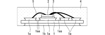
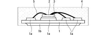
本発明の実施の形態を説明する前に、本発明の前提となる技術について説明する。図10は、前提技術における半導体装置の断面図である。図10に示すように、前提技術における半導体装置のセラミック基板1の表面には複数の回路パターン1aが配置されている。少なくとも1つの回路パターン1aの表面には、半導体素子2がはんだ3により接合されて実装されている。半導体素子2の電極と他の回路パターン1aとは、アルミワイヤ5によって電気的に接続されている。また、回路パターン1aは、図示しない端子とはんだや溶接により接合され外部の端子と電気的に接続されている。セラミック基板1の裏面(即ち回路パターン1aが配置される面と反対側の面)には、裏面パターン1bが形成されている。なお、回路パターン1aの材質は、一般的にアルミニウムや銅である。
<Prerequisite technology>
Prior to the description of the embodiments of the present invention, the technology that is the premise of the present invention will be described. FIG. 10 is a cross-sectional view of a semiconductor device in the base technology. As shown in FIG. 10, a plurality of
セラミック基板1、回路パターン1a、半導体素子2およびアルミワイヤ5は封止樹脂4により封止されている。封止樹脂4とは、例えばエポキシ樹脂である。なお、裏面パターン1bは封止樹脂により封止されず、半導体装置下面に露出している。
The
以上で説明した半導体装置は、例えば電気自動車や電車等のモータを制御するインバータや回生用のコンバータとして使用される。 The semiconductor device described above is used as, for example, an inverter for controlling a motor such as an electric car or a train, or a converter for regeneration.
前提技術における半導体装置は以上のように構成されているので、セラミック基板1を小型化するためには、回路パターン1aの面積を減らすか、回路パターン1a間の絶縁部の幅を狭める必要があり、組立性の悪化および絶縁性の低下の問題があった。
Since the semiconductor device in the base technology is configured as described above, in order to reduce the size of the
また、封止樹脂4と、セラミック基板1および回路パターン1aとの密着性が悪いため剥離が生じる問題があった。封止樹脂4の剥離が生じると、封止樹脂4で保持している構造物(例えばアルミワイヤや端子)の接合寿命低下、また、セラミック基板1上の回路パターン1a間の絶縁性の低下などが生じる問題があった。
Further, there is a problem that peeling occurs because the adhesion between the
<実施の形態1>
<構成>
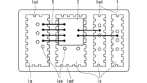
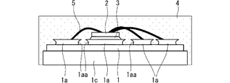
図1は、本実施の形態における半導体装置の断面図である。図2は、本実施の形態における半導体装置の断面の部分拡大図である。図2は、より詳しくは図1の断面図において回路パターン1a側面の断面を拡大した図である。また、図3は、本実施の形態における半導体装置の平面図である。
<
<Configuration>
FIG. 1 is a cross-sectional view of the semiconductor device according to the present embodiment. FIG. 2 is a partially enlarged view of a cross section of the semiconductor device according to the present embodiment. More specifically, FIG. 2 is an enlarged view of the cross section of the side surface of the
本実施の形態の半導体装置において、セラミック基板1の表面には複数の回路パターン1aが配置されている。少なくとも1つの回路パターン1aの表面には、半導体素子2がはんだ3により接合されて実装されている。
In the semiconductor device according to the present embodiment, a plurality of
図1に示すように、互いに隣接する回路パターン1aの対向する側面には、アンダーカット部1aaが形成されている。図2にアンダーカット部1aaの拡大図を示す。アンダーカット部1aaにおいて、回路パターン1aのセラミック基板1に接する面の端部12よりも、回路パターン1aの表面の端部11の方が、回路パターン1aの外側に突出している。アンダーカット部1aaにも封止樹脂4が充填されている。なお、回路パターン1aにおいて、他の回路パターン1aと対向しない側面にもアンダーカット部1aaを形成してもよい。
As shown in FIG. 1, undercut portions 1aa are formed on opposite side surfaces of
図3を用いて、本実施の形態における半導体装置の回路パターン1aの平面形状について説明する。回路パターン1aには、回路パターン1aの外周に沿って平面視で凹凸1adが形成されている。凹凸1adは封止樹脂4で封止されている。また、回路パターン1a表面には穴1aeが形成されており、穴1aeにも封止樹脂4が充填されている。図2に示すように、凹凸1adの側面にはアンダーカット部1aaが形成されている。また、穴1aeの側面にもアンダーカット部1aaを形成してもよい。
The planar shape of the
なお、本実施の形態において半導体素子2は、例えば炭化珪素(SiC)、窒化ガリウム(GaN)などのワイドバンドギャップ半導体を含む絶縁ゲートバイポーラトランジスタ(IGBT)である。
In the present embodiment, the
<製造方法>
本実施の形態における半導体装置の製造方法について説明する。まず、セラミック基板1の表面に金属膜を形成する。金属膜は、厚さが、例えば0.1〜2mmの金属箔をセラミック基板1の表面に貼り付けることで形成される。また、セラミック基板1の裏面には裏面パターン1bが形成される。
<Manufacturing method>
A method for manufacturing a semiconductor device in the present embodiment will be described. First, a metal film is formed on the surface of the
次に、金属膜をエッチングすることにより回路パターン1aを形成する。エッチングを行う際に、回路パターン1aの側面をオーバーエッチングすることにより、アンダーカット部1aaが形成される。エッチングの時間や噴射などの条件を調整することによって、回路パターン1aの側面がR形状にえぐれ、回路パターン1aのセラミック基板1に接する面の端部12よりも、回路パターン1aの表面の端部11の方が外側に突出したアンダーカット部1aaを形成することが可能である。
Next, the
次に、回路パターン1aの所定の位置に、はんだ3を介して半導体素子2が実装される。また、他の回路パターン1aと半導体素子2の電極とは、例えばワイヤボンディング法によってアルミワイヤ5で接続される。
Next, the
さらに、セラミック基板1、回路パターン1a、半導体素子2およびアルミワイヤ5は封止樹脂4(例えばエポキシ樹脂)により封止される。樹脂封止は、例えばトランスファーモールド法により行われる。なお、裏面パターン1bの表面は封止されず、半導体装置下面から露出している。以上の工程により、本実施の形態における半導体装置が製造される。
Further, the
<作用>
以上で述べたように、本実施の形態における半導体装置は、セラミック基板1表面に配置した回路パターン1aに、はんだ3等のロウ材により半導体素子2を接合し、また、半導体素子2と他の回路パターン1aは、アルミワイヤにより接続される。回路パターン1aはセラミック基板上で回路配線されて、外部端子へとはんだやワイヤボンドにより電気的に接続される。
<Action>
As described above, in the semiconductor device according to the present embodiment, the
従って、半導体装置の小型化のためにセラミック基板1の面積を縮小するには、それぞれの回路パターン1aの機能上必要な面積および幅を確保する必要がある。そして、それぞれの回路パターン1a間には、半導体装置の動作時に数百ボルトから千ボルト以上の電位差が生じることがある。封止樹脂4とセラミック基板1との界面での放電を防止するために、回路パターン1a間には、絶縁に必要な間隔を設ける必要がある。
Therefore, in order to reduce the area of the
そこで、本実施の形態では、隣接する回路パターン1aの対向する側面にアンダーカット部1aaを設ける。アンダーカット部1aaを設けることにより、回路パターン1aの表面の面積を縮小することなく、回路パターン1aの底面の面積を縮小することが可能である。つまり、回路パターン1aの底面の面積が縮小することにより、セラミック基板1の表面において、隣接する回路パターン1aの間隔が広くなるため、絶縁性が向上する。よって、アンダーカット部1aaを設けない前提技術と同程度の絶縁性を想定して半導体装置を設計する場合は、前提技術と比較して、複数の回路パターン1aをより近接して配置することが可能となるため、回路パターン1aを配置するセラミック基板1の面積を縮小することが可能となる。
Therefore, in the present embodiment, the undercut portions 1aa are provided on the side surfaces of the
また、一般に、半導体装置は環境温度の変化や半導体素子の発熱によって、半導体装置を構成する部品それぞれが、温度変化量と線膨張係数を掛け合わせた分だけ膨張、収縮をする。そのため、それぞれの部品の界面にはひずみが発生し、特にひずみの大きい部分や接着強度の低い部分には剥離や亀裂が生じる。エポキシ樹脂は、その製造工程において線膨張係数をコントロールすることができるが、例えば、銅(線膨張係数16.7ppm/℃)にエポキシ樹脂の線膨張係数を合わせると、エポキシ樹脂とセラミック(4〜7ppm/℃)との線膨張係数の差は大きくなり、その逆もある。さらに、エポキシ樹脂とセラミック、銅、アルミニウムは元々、接着性が良くないため、接着界面にポリイミド等の低ヤング率樹脂を予め塗布してから樹脂封止を行わないと、冷熱サイクルによって、界面剥離が生じ易い。 In general, in a semiconductor device, each component constituting the semiconductor device expands and contracts by a product of a temperature change amount and a linear expansion coefficient due to a change in environmental temperature and heat generation of a semiconductor element. Therefore, distortion occurs at the interface of each component, and peeling or cracking occurs particularly in a portion where the strain is large or a portion where the adhesive strength is low. The epoxy resin can control the linear expansion coefficient in the production process. For example, when the linear expansion coefficient of the epoxy resin is matched with copper (linear expansion coefficient 16.7 ppm / ° C.), the epoxy resin and the ceramic (4˜ The difference in linear expansion coefficient from 7 ppm / ° C. is large and vice versa. In addition, since epoxy resin and ceramic, copper, and aluminum originally do not have good adhesion, if the resin interface is not sealed after applying a low Young's modulus resin such as polyimide to the bonding interface, the interface will peel off due to the thermal cycle. Is likely to occur.
そこで、本実施の形態における半導体装置では、回路パターン1aの側面にアンダーカット部1aaを設け、アンダーカット部1aaを封止樹脂4(エポキシ樹脂)で充填する。アンダーカット部1aaに封止樹脂が噛み込むことにより、セラミック基板1と封止樹脂4との剥離を防止することができる。セラミック基板1の面積に対し、封止樹脂4を噛み込ませるためのアンダーカット部1aaが多いほど、剥離防止の効果が高くなる。セラミック基板1と封止樹脂4の密着性が向上すれば、外部からの水分やイオンの浸入が抑制されるため、半導体素子2および、アルミワイヤ5の接合部の信頼性も向上するため、半導体装置の信頼性が向上する。
Therefore, in the semiconductor device according to the present embodiment, the undercut portion 1aa is provided on the side surface of the
<第1の変形例>
図4は、本実施の形態における半導体装置の第1の変形例の断面図である。本変形例は、セラミック基板1の裏面に金属ベース1cが一体接合されている。その他の構成は実施の形態1(図1)と同じため、説明を省略する。セラミック基板1の裏面には、裏面パターン1bに代えて金属ベース1cが接合されていても、前述したセラミック基板1の面積縮小および半導体装置の信頼性向上の効果を得ることが可能である。
<First Modification>
FIG. 4 is a cross-sectional view of a first modification of the semiconductor device according to the present embodiment. In this modification, a
<第2の変形例>
図5は、本実施の形態における半導体装置の第2の変形例の断面図である。本変形例は、セラミック基板1の裏面に放熱フィン1dが一体接合されている。その他の構成は実施の形態1(図1)と同じため、説明を省略する。セラミック基板1の裏面には、裏面パターン1bに代えて放熱フィン1dが接合されていても、前述したセラミック基板1の面積縮小および半導体装置の信頼性向上の効果を得ることが可能である。
<Second Modification>
FIG. 5 is a cross-sectional view of a second modification of the semiconductor device according to the present embodiment. In this modification, the
<第3の変形例>
図6は、本実施の形態における半導体装置の第3の変形例の断面図である。本変形例は、実施の形態1(図1)の半導体装置において、裏面パターン1bをはんだ3を介して放熱フィン6に接合したものである。その他の構成は実施の形態1(図1)と同じため、説明を省略する。セラミック基板1の裏面には、裏面パターン1bにさらに放熱フィン1dが接合されていても、前述したセラミック基板1の面積縮小および半導体装置の信頼性向上の効果を得ることが可能である。
<Third Modification>
FIG. 6 is a cross-sectional view of a third modification of the semiconductor device according to the present embodiment. In this modification, in the semiconductor device of the first embodiment (FIG. 1), the
<第4の変形例>
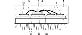
図7は、本実施の形態における半導体装置の第4の変形例の断面図である。本変形例は、セラミック基板1の裏面に放熱フィン1dが一体接合されている。さらに、放熱フィン1dの上面側にはセラミック基板1、回路パターン1a、半導体素子2およびアルミワイヤ5を囲むように樹脂製のケース7が固定されている。
<Fourth Modification>
FIG. 7 is a cross-sectional view of a fourth modification of the semiconductor device in the present embodiment. In this modification, the
ケース7内部に封止樹脂4(例えばエポキシ樹脂)が注入され、硬化することで、セラミック基板1、回路パターン1a、半導体素子2およびアルミワイヤ5が封止樹脂4により封止される。封止樹脂4は、回路パターン1aのアンダーカット部1aaにも充填される。
The sealing resin 4 (for example, epoxy resin) is injected into the
その他の構成は実施の形態1(図1)と同じため、説明を省略する。半導体装置がケース7を備え、ケース7に注入された封止樹脂4によりケース7内部を封止する構成であっても、前述したセラミック基板1の面積縮小および半導体装置の信頼性向上の効果を得ることが可能である。
Since other configurations are the same as those of the first embodiment (FIG. 1), description thereof is omitted. Even if the semiconductor device includes the
<効果>
本実施の形態における半導体装置は、セラミック基板1と、セラミック基板1表面に配置された複数の回路パターン1aと、少なくとも1つの回路パターン1aの表面に配置された半導体素子2と、セラミック基板1、複数の回路パターン1aおよび半導体素子2を封止する封止樹脂4と、を備え、隣接する回路パターン1aの対向する側面にはアンダーカット部1aaが形成され、アンダーカット部1aaにおいて、回路パターン1aのセラミック基板1に接する面の端部12よりも、回路パターン1aの表面の端部11の方が回路パターン1aの外側に突出しており、アンダーカット部1aaにも封止樹脂4が充填されることを特徴とする。
<Effect>
The semiconductor device according to the present embodiment includes a
従って、隣接する回路パターン1aの対向する側面にアンダーカット部1aaを設けることにより、回路パターン1aの表面の面積を縮小することなく、回路パターン1aの底面の面積を縮小することが可能である。よって、回路パターン1a表面の機能的に必要な面積を確保し、かつ、絶縁に必要な回路パターン1a間の間隔を確保することができる。つまり、絶縁性を低下させることなく、隣接する回路パターン1aの間隔をより狭くすることが可能なため、回路パターン1aが形成されるセラミック基板1の面積を縮小することが可能である。セラミック基板1の面積縮小により、半導体装置の小型化が可能である。
Therefore, by providing the undercut portion 1aa on the opposite side surface of the
また、回路パターン1aの側面にアンダーカット部1aaを設けることにより、アンダーカット部1aaに封止樹脂4が充填され、セラミック基板1と封止樹脂4の密着性が向上するため、封止樹脂4の剥離が抑制され、半導体装置の信頼性が向上する。つまり、アンダーカット部1aaを設けることにより、絶縁性の向上による半導体装置の小型化と、剥離の抑制による信頼性の向上の2つの効果を同時に得ることが可能である。
Also, by providing the undercut portion 1aa on the side surface of the
また、本実施の形態における半導体装置の製造方法は、(a)セラミック基板1の表面に金属膜を形成する工程と、(b)金属膜をエッチングして回路パターン1aを形成する工程と、を備え、工程(b)において、回路パターン1aの側面をオーバーエッチングすることにより、アンダーカット部1aaを形成することを特徴とする。
The method for manufacturing a semiconductor device in the present embodiment includes (a) a step of forming a metal film on the surface of the
従って、本実施の形態では、エッチングにより回路パターン1aを形成する工程において、同時にアンダーカット部1aaを形成する。よって、製造工程数を増やすことなくアンダーカット部1aaを形成することが可能である。製造工程を増やすことなく、アンダーカット部1aaを設けることが可能なため、製造コストを増大させることなく、絶縁性の向上による半導体装置の小型化および剥離抑制による半導体装置の信頼性の向上の2つの効果を得ることが可能である。
Accordingly, in the present embodiment, the undercut portion 1aa is simultaneously formed in the step of forming the
また、本実施の形態における半導体装置において、回路パターン1aには、回路パターン1aの外周に沿って平面視で凹凸1adが形成されており、当該凹凸1adも封止樹脂4で封止されることを特徴とする。
Further, in the semiconductor device according to the present embodiment, the
従って、回路パターン1aの外周に沿って凹凸1adを形成することによって、回路パターン1aが封止樹脂4に接触する面積が増大する。接触面積が増大することによって、回路パターン1aと封止樹脂4との密着性が向上するため、半導体装置の信頼性が向上する。
Accordingly, by forming the unevenness 1ad along the outer periphery of the
また、本実施の形態における半導体装置において、回路パターン1a表面に穴1aeが形成されており、当該穴1aeにも封止樹脂4が充填されることを特徴とする。
Further, the semiconductor device according to the present embodiment is characterized in that a hole 1ae is formed on the surface of the
従って、回路パターン1a表面に穴1aeを形成することによって、回路パターン1aが封止樹脂4に接触する面積が増大する。接触面積が増大することによって、回路パターン1aと封止樹脂4との密着性が向上するため、半導体装置の信頼性が向上する。
Therefore, by forming the hole 1ae on the surface of the
また、本実施の形態における半導体装置において、半導体素子2はワイドバンドギャップ半導体を含むことを特徴とする。
In the semiconductor device in this embodiment, the
従って、本実施の形態では、例えば炭化珪素(SiC)、窒化ガリウム(GaN)などのワイドバンドギャップ半導体により半導体素子2を構成する。例えばSiC半導体素子は高温下での高速なスイッチング動作が可能な大電力用途の半導体装置に適用されるため、半導体装置を大型化することなく絶縁性を保てる本発明が特に有効である。また、大電力用途の半導体装置は高温下で動作するため、封止樹脂4の剥離を抑制して半導体装置の信頼性を向上させた本発明が特に有効である。
Therefore, in the present embodiment, the
<実施の形態2>
<構成>
図8は、本実施の形態における半導体装置の断面の部分拡大図である。本実施の形態における半導体装置において、互いに隣接する回路パターン1aの対向する側面には、実施の形態1において説明したアンダーカット部1aa(図2)に類似した形状のアンダーカット部1abが形成されている。図8にアンダーカット部1aaの拡大図を示す。
<
<Configuration>
FIG. 8 is a partial enlarged view of a cross section of the semiconductor device according to the present embodiment. In the semiconductor device according to the present embodiment, undercut portions 1ab having a shape similar to the undercut portion 1aa (FIG. 2) described in the first embodiment are formed on opposing side surfaces of the
図8に示すように、アンダーカット部1abにおいて、回路パターン1aのセラミック基板1に接する面の端部12よりも、回路パターン1aの表面の端部11の方が外側に突出している。アンダーカット部1abにも封止樹脂4が充填されている。実施の形態1におけるアンダーカット部1aaはエッチングにより形成されたR形状であったが、本実施の形態におけるアンダーカット部1abは、プレス加工により形成されるため直線的な形状となる。その他の構成は実施の形態1と同じであるため、同じ部分については説明を省略する。
As shown in FIG. 8, in the undercut portion 1ab, the
<製造方法>
本実施の形態における半導体装置の製造方法について説明する。まず、金属板をプレス加工により打ち抜いて、回路パターン1aを形成する。次に、回路パターン1a下面(即ち、セラミック基板1に接する面)の端部の任意の箇所をプレスすることにより、アンダーカット部1abを形成する。そして、アンダーカット部1abが形成された回路パターン1aをセラミック基板1の表面に貼り付ける。
<Manufacturing method>
A method for manufacturing a semiconductor device in the present embodiment will be described. First, a metal plate is punched out by press working to form a
裏面パターン1bを形成する工程、半導体素子2の実装工程、アルミワイヤ5による配線工程、封止樹脂4による封止工程は実施の形態1と同じため説明を省略する。
Since the step of forming the
<効果>
本実施の形態における半導体装置の製造方法は、(c)金属板を打ち抜いて回路パターン1aを形成する工程と、(d)工程(c)の後、回路パターン1aの端部をプレスすることによりアンダーカット部1abを形成する工程と、(e)工程(d)の後、回路パターン1aをセラミック基板1の表面に貼り付ける工程と、を備える。
<Effect>
The manufacturing method of the semiconductor device in the present embodiment includes (c) a step of punching a metal plate to form a
従って、プレスする箇所を選択することで、回路パターン1aの周囲の全てにアンダーカット部1abを形成するのではなく、回路パターン1aの周囲の任意の箇所にアンダーカット部1abを形成することが可能となる。よって、実施の形態1で述べた効果に加えて、アンダーカット部1abを形成する位置の自由度が向上する。
Therefore, by selecting the place to be pressed, it is possible to form the undercut portion 1ab at any location around the
<実施の形態3>
<構成>
図9は、本実施の形態における半導体装置の断面の部分拡大図である。本実施の形態における半導体装置において、互いに隣接する回路パターン1aの対向する側面には、実施の形態1において説明したアンダーカット部1aa(図2)に類似した形状のアンダーカット部1afが形成されている。図9にアンダーカット部1afの拡大図を示す。
<
<Configuration>
FIG. 9 is a partially enlarged view of a cross section of the semiconductor device according to the present embodiment. In the semiconductor device according to the present embodiment, an undercut portion 1af having a shape similar to the undercut portion 1aa (FIG. 2) described in the first embodiment is formed on the opposing side surfaces of the
図9に示すように、アンダーカット部1afにおいて、回路パターン1aのセラミック基板1に接する面の端部12よりも、回路パターン1aの表面の端部11の方が外側に突出している。アンダーカット部1afにも封止樹脂4が充填されている。
As shown in FIG. 9, in the undercut portion 1af, the
また、回路パターン1aの表面には、回路パターン1aの表面の端部11に沿って溝1acが形成されている。回路パターン1aの表面の端部11から溝1acまでの距離は、回路パターン1aの厚み以下である。なお、溝1acにも封止樹脂4が充填されている。その他の構成は実施の形態1と同じであるため、同じ部分については説明を省略する。
A groove 1ac is formed on the surface of the
<製造方法>
本実施の形態における半導体装置の製造方法について説明する。まず、セラミック基板1の表面に回路パターン1aを形成する。回路パターン1aは、エッチングにより形成してもよいし、金属板をプレス加工により打ち抜いて回路パターン1aを形成してセラミック基板1の表面に貼り付けてもよい。
<Manufacturing method>
A method for manufacturing a semiconductor device in the present embodiment will be described. First, the
次に、回路パターン1aの表面の端部11に沿って、回路パターン1aの表面に対して圧力を加えることで溝1acを形成する。ここで、圧力を加える位置は、回路パターン1aの表面の端部11から回路パターン1aの厚み以下の距離である。
Next, a groove 1ac is formed by applying pressure to the surface of the
端部11から回路パターン1aの厚み以下の距離の位置において圧力を加えることにより、溝1acが形成されるときに、回路パターン1aの表面の端部11が外側に押し出され、アンダーカット部1afが形成される。
By applying pressure at a distance equal to or less than the thickness of the
裏面パターン1bを形成する工程、半導体素子2の実装工程、アルミワイヤ5による配線工程、封止樹脂4による封止工程は実施の形態1と同じため説明を省略する。なお、封止工程において、溝1acにも封止樹脂4が充填される。
Since the step of forming the
<効果>
本実施の形態における半導体装置において、回路パターン1aの表面には、回路パターン1aの表面の端部11に沿って溝1acが形成され、回路パターン1aの表面の端部11から溝1acまでの距離は、回路パターン1aの厚み以下であり、溝1acにも封止樹脂4が充填されることを特徴とする。
<Effect>
In the semiconductor device according to the present embodiment, a groove 1ac is formed on the surface of the
従って、回路パターン1aの側面にアンダーカット部1afを設けることにより、実施の形態1で述べた様に、絶縁性を低下させることなく、回路パターン1a間の間隔をより狭くすることが可能である。よって、回路パターン1aが形成されるセラミック基板1の面積を縮小することが可能であり、半導体装置の小型化が可能となる。
Therefore, by providing the undercut portion 1af on the side surface of the
また、回路パターン1aの側面にアンダーカット部1afを設けることにより、アンダーカット部1afに封止樹脂4が充填され、セラミック基板1と封止樹脂4の密着性が向上するため、封止樹脂4の剥離が抑制され、半導体装置の信頼性が向上する。また、本実施の形態では、回路パターン1aの表面に溝1acが形成されるため、回路パターン1aが封止樹脂4に接触する面積が増大する。接触面積が増大することによって、回路パターン1aと封止樹脂4との密着性が向上するため、半導体装置の信頼性がより向上する。
Further, by providing the undercut portion 1af on the side surface of the
また、本実施の形態における半導体装置の製造方法は、(f)回路パターン1aをセラミック基板1表面に形成する工程と、(g)工程(f)の後、回路パターン1aの表面の端部11に沿って回路パターン1aの表面に対して圧力を加えて溝1acを形成する工程と、を備え、工程(g)において、圧力を加える位置は、回路パターン1aの表面の端部11から回路パターン1aの厚み以下の距離であり、溝1acが形成されるときに、回路パターン1aの表面の端部11が外側に押し出され、アンダーカット部1afが形成されることを特徴とする。
Further, in the method of manufacturing a semiconductor device according to the present embodiment, (f) a step of forming the
従って、溝1acを形成する箇所を選択することで、回路パターン1aの周囲全てにアンダーカット部1afを形成するのではなく、回路パターン1aの周囲の任意の箇所にアンダーカット部1afを形成することが可能となる。さらに、アンダーカット部1afを形成するために、回路パターン1aの表面には溝1acが形成されるため、回路パターン1aが封止樹脂4に接触する面積が増大する。接触面積が増大することによって、回路パターン1aと封止樹脂4との密着性が向上するため、半導体装置の信頼性がより向上する。
Therefore, by selecting a location where the groove 1ac is to be formed, the undercut portion 1af is not formed around the
なお、本発明は、その発明の範囲内において、各実施の形態を自由に組み合わせたり、各実施の形態を適宜、変形、省略することが可能である。 It should be noted that the present invention can be freely combined with each other within the scope of the invention, and each embodiment can be appropriately modified or omitted.
1 セラミック基板、1a 回路パターン、1aa,1ab,1af アンダーカット部、1ac 溝、1ad 凹凸、1ae 穴、1b 裏面パターン、1c 金属ベース、1d,6 放熱フィン、2 半導体素子、3 はんだ、4 封止樹脂、5 アルミワイヤ、7 ケース、11,12 端部。
DESCRIPTION OF
Claims (6)
前記セラミック基板表面に配置された複数の回路パターンと、
少なくとも1つの前記回路パターンの表面に配置された半導体素子と、
前記セラミック基板、前記複数の回路パターンおよび前記半導体素子を封止する封止樹脂と、
を備え、
隣接する前記回路パターンの対向する側面にはアンダーカット部が形成され、
前記アンダーカット部において、前記回路パターンの前記セラミック基板に接する面の端部よりも、前記回路パターンの表面の端部の方が当該回路パターンの外側に突出しており、かつ、前記回路パターンの前記セラミック基板に接する前記面と前記回路パターンの前記表面との間に凹部が設けられ、
前記アンダーカット部にも前記封止樹脂が充填されることを特徴とする、
半導体装置。 A ceramic substrate;
A plurality of circuit patterns disposed on the surface of the ceramic substrate;
A semiconductor element disposed on a surface of at least one of the circuit patterns;
A sealing resin for sealing the ceramic substrate, the plurality of circuit patterns, and the semiconductor element;
With
Undercut portions are formed on the opposite side surfaces of the adjacent circuit patterns,
In the undercut portion, the end portion of the surface of the circuit pattern protrudes outside the circuit pattern rather than the end portion of the surface contacting the ceramic substrate of the circuit pattern, and the circuit pattern A recess is provided between the surface in contact with the ceramic substrate and the surface of the circuit pattern,
The undercut portion is also filled with the sealing resin,
Semiconductor device.
(a)前記セラミック基板の表面に金属膜を形成する工程と、
(b)前記金属膜をエッチングして前記回路パターンを形成する工程と、
を備え、
前記工程(b)において、前記回路パターンの側面をオーバーエッチングすることにより、前記アンダーカット部を形成することを特徴とする、
半導体装置の製造方法。 A manufacturing method for manufacturing the semiconductor device according to claim 1,
(A) forming a metal film on the surface of the ceramic substrate;
(B) etching the metal film to form the circuit pattern;
With
In the step (b), the undercut portion is formed by over-etching the side surface of the circuit pattern.
A method for manufacturing a semiconductor device.
(c)金属板を打ち抜いて前記回路パターンを形成する工程と、
(d)前記工程(c)の後、前記回路パターンの端部をプレスすることにより前記アンダーカット部を形成する工程と、
(e)前記工程(d)の後、前記回路パターンを前記セラミック基板の表面に貼り付ける工程と、
を備える、
半導体装置の製造方法。 A manufacturing method for manufacturing the semiconductor device according to claim 1,
(C) punching a metal plate to form the circuit pattern;
(D) after the step (c), forming the undercut portion by pressing an end portion of the circuit pattern;
(E) After the step (d), a step of attaching the circuit pattern to the surface of the ceramic substrate;
Comprising
A method for manufacturing a semiconductor device.
請求項1に記載の半導体装置。 In the circuit pattern, irregularities are formed in a plan view along the outer periphery of the circuit pattern, and the irregularities are also sealed with the sealing resin,
The semiconductor device according to claim 1.
請求項1又は請求項4に記載の半導体装置。 A hole is formed on the surface of the circuit pattern, and the hole is filled with the sealing resin.
The semiconductor device according to claim 1.
請求項1、請求項4、請求項5のいずれかに記載の半導体装置。 The semiconductor element includes a wide band gap semiconductor,
The semiconductor device according to claim 1, claim 4, or claim 5.
Priority Applications (1)
| Application Number | Priority Date | Filing Date | Title |
|---|---|---|---|
| JP2017157093A JP2017201726A (en) | 2017-08-16 | 2017-08-16 | Semiconductor device and manufacturing method of the same |
Applications Claiming Priority (1)
| Application Number | Priority Date | Filing Date | Title |
|---|---|---|---|
| JP2017157093A JP2017201726A (en) | 2017-08-16 | 2017-08-16 | Semiconductor device and manufacturing method of the same |
Related Parent Applications (1)
| Application Number | Title | Priority Date | Filing Date |
|---|---|---|---|
| JP2013202995A Division JP6210818B2 (en) | 2013-09-30 | 2013-09-30 | Semiconductor device and manufacturing method thereof |
Publications (1)
| Publication Number | Publication Date |
|---|---|
| JP2017201726A true JP2017201726A (en) | 2017-11-09 |
Family
ID=60264751
Family Applications (1)
| Application Number | Title | Priority Date | Filing Date |
|---|---|---|---|
| JP2017157093A Pending JP2017201726A (en) | 2017-08-16 | 2017-08-16 | Semiconductor device and manufacturing method of the same |
Country Status (1)
| Country | Link |
|---|---|
| JP (1) | JP2017201726A (en) |
Citations (8)
| Publication number | Priority date | Publication date | Assignee | Title |
|---|---|---|---|---|
| JPS62252159A (en) * | 1986-04-25 | 1987-11-02 | Hitachi Ltd | Lead frame for semiconductor device |
| JPH0613501A (en) * | 1992-06-29 | 1994-01-21 | Fuji Electric Co Ltd | Resin-sealed semiconductor device |
| JPH0645346U (en) * | 1992-11-24 | 1994-06-14 | 松下電工株式会社 | Semiconductor device |
| JPH06252534A (en) * | 1993-02-23 | 1994-09-09 | Matsushita Electric Works Ltd | Printed wiring board with sealing and its manufacture |
| JPH07161911A (en) * | 1993-12-10 | 1995-06-23 | Nec Corp | Resin-sealed semiconductor device |
| JP2000277809A (en) * | 1999-03-24 | 2000-10-06 | Rohm Co Ltd | Chip type light emitting device |
| JP2006032617A (en) * | 2004-07-15 | 2006-02-02 | Hitachi Ltd | Semiconductor power module |
| JP2015070107A (en) * | 2013-09-30 | 2015-04-13 | 三菱電機株式会社 | Semiconductor device and manufacturing method of the same |
-
2017
- 2017-08-16 JP JP2017157093A patent/JP2017201726A/en active Pending
Patent Citations (8)
| Publication number | Priority date | Publication date | Assignee | Title |
|---|---|---|---|---|
| JPS62252159A (en) * | 1986-04-25 | 1987-11-02 | Hitachi Ltd | Lead frame for semiconductor device |
| JPH0613501A (en) * | 1992-06-29 | 1994-01-21 | Fuji Electric Co Ltd | Resin-sealed semiconductor device |
| JPH0645346U (en) * | 1992-11-24 | 1994-06-14 | 松下電工株式会社 | Semiconductor device |
| JPH06252534A (en) * | 1993-02-23 | 1994-09-09 | Matsushita Electric Works Ltd | Printed wiring board with sealing and its manufacture |
| JPH07161911A (en) * | 1993-12-10 | 1995-06-23 | Nec Corp | Resin-sealed semiconductor device |
| JP2000277809A (en) * | 1999-03-24 | 2000-10-06 | Rohm Co Ltd | Chip type light emitting device |
| JP2006032617A (en) * | 2004-07-15 | 2006-02-02 | Hitachi Ltd | Semiconductor power module |
| JP2015070107A (en) * | 2013-09-30 | 2015-04-13 | 三菱電機株式会社 | Semiconductor device and manufacturing method of the same |
Similar Documents
| Publication | Publication Date | Title |
|---|---|---|
| JP6210818B2 (en) | Semiconductor device and manufacturing method thereof | |
| JP4635564B2 (en) | Semiconductor device | |
| US9171773B2 (en) | Semiconductor device | |
| JP5656907B2 (en) | Power module | |
| JP6300633B2 (en) | Power module | |
| JP6305302B2 (en) | Semiconductor device and manufacturing method thereof | |
| US9754855B2 (en) | Semiconductor module having an embedded metal heat dissipation plate | |
| JP2016018866A (en) | Power module | |
| JP6125089B2 (en) | Power semiconductor module and power unit | |
| JP2019067886A (en) | Semiconductor device | |
| JP2010283053A (en) | Semiconductor device and manufacturing method thereof | |
| CN111354709A (en) | Semiconductor device and method for manufacturing the same | |
| JP5218009B2 (en) | Semiconductor device | |
| JP2012015222A (en) | Semiconductor device | |
| JP6305176B2 (en) | Semiconductor device and manufacturing method | |
| CN111354710B (en) | Semiconductor device and manufacturing method thereof | |
| JP2014013878A (en) | Electronic apparatus | |
| JP4046623B2 (en) | Power semiconductor module and fixing method thereof | |
| JP2010232365A (en) | Semiconductor device | |
| JP7332528B2 (en) | Semiconductor device and method for manufacturing semiconductor device | |
| JP2017201726A (en) | Semiconductor device and manufacturing method of the same | |
| JP7118205B1 (en) | Semiconductor device and semiconductor module using the same | |
| JP2019040955A (en) | Manufacturing method of semiconductor module | |
| JP2023127609A (en) | semiconductor equipment | |
| JP6844166B2 (en) | Semiconductor device |
Legal Events
| Date | Code | Title | Description |
|---|---|---|---|
| A621 | Written request for application examination |
Free format text: JAPANESE INTERMEDIATE CODE: A621 Effective date: 20170816 |
|
| A977 | Report on retrieval |
Free format text: JAPANESE INTERMEDIATE CODE: A971007 Effective date: 20180223 |
|
| A131 | Notification of reasons for refusal |
Free format text: JAPANESE INTERMEDIATE CODE: A131 Effective date: 20180403 |
|
| A521 | Request for written amendment filed |
Free format text: JAPANESE INTERMEDIATE CODE: A523 Effective date: 20180509 |
|
| A02 | Decision of refusal |
Free format text: JAPANESE INTERMEDIATE CODE: A02 Effective date: 20181106 |