JP2017201729A - Side-emitting type light emitting device - Google Patents
Side-emitting type light emitting device Download PDFInfo
- Publication number
- JP2017201729A JP2017201729A JP2017157215A JP2017157215A JP2017201729A JP 2017201729 A JP2017201729 A JP 2017201729A JP 2017157215 A JP2017157215 A JP 2017157215A JP 2017157215 A JP2017157215 A JP 2017157215A JP 2017201729 A JP2017201729 A JP 2017201729A
- Authority
- JP
- Japan
- Prior art keywords
- wall
- cavity
- package body
- light emitting
- emitting device
- Prior art date
- Legal status (The legal status is an assumption and is not a legal conclusion. Google has not performed a legal analysis and makes no representation as to the accuracy of the status listed.)
- Granted
Links
Images



Classifications
-
- H—ELECTRICITY
- H10—SEMICONDUCTOR DEVICES; ELECTRIC SOLID-STATE DEVICES NOT OTHERWISE PROVIDED FOR
- H10H—INORGANIC LIGHT-EMITTING SEMICONDUCTOR DEVICES HAVING POTENTIAL BARRIERS
- H10H20/00—Individual inorganic light-emitting semiconductor devices having potential barriers, e.g. light-emitting diodes [LED]
- H10H20/80—Constructional details
- H10H20/85—Packages
- H10H20/8506—Containers
-
- G—PHYSICS
- G02—OPTICS
- G02B—OPTICAL ELEMENTS, SYSTEMS OR APPARATUS
- G02B6/00—Light guides; Structural details of arrangements comprising light guides and other optical elements, e.g. couplings
- G02B6/0001—Light guides; Structural details of arrangements comprising light guides and other optical elements, e.g. couplings specially adapted for lighting devices or systems
- G02B6/0011—Light guides; Structural details of arrangements comprising light guides and other optical elements, e.g. couplings specially adapted for lighting devices or systems the light guides being planar or of plate-like form
- G02B6/0013—Means for improving the coupling-in of light from the light source into the light guide
- G02B6/0023—Means for improving the coupling-in of light from the light source into the light guide provided by one optical element, or plurality thereof, placed between the light guide and the light source, or around the light source
- G02B6/0031—Reflecting element, sheet or layer
-
- G—PHYSICS
- G02—OPTICS
- G02B—OPTICAL ELEMENTS, SYSTEMS OR APPARATUS
- G02B6/00—Light guides; Structural details of arrangements comprising light guides and other optical elements, e.g. couplings
- G02B6/0001—Light guides; Structural details of arrangements comprising light guides and other optical elements, e.g. couplings specially adapted for lighting devices or systems
- G02B6/0011—Light guides; Structural details of arrangements comprising light guides and other optical elements, e.g. couplings specially adapted for lighting devices or systems the light guides being planar or of plate-like form
- G02B6/0066—Light guides; Structural details of arrangements comprising light guides and other optical elements, e.g. couplings specially adapted for lighting devices or systems the light guides being planar or of plate-like form characterised by the light source being coupled to the light guide
- G02B6/0073—Light emitting diode [LED]
-
- H—ELECTRICITY
- H10—SEMICONDUCTOR DEVICES; ELECTRIC SOLID-STATE DEVICES NOT OTHERWISE PROVIDED FOR
- H10H—INORGANIC LIGHT-EMITTING SEMICONDUCTOR DEVICES HAVING POTENTIAL BARRIERS
- H10H20/00—Individual inorganic light-emitting semiconductor devices having potential barriers, e.g. light-emitting diodes [LED]
- H10H20/80—Constructional details
- H10H20/81—Bodies
- H10H20/822—Materials of the light-emitting regions
- H10H20/824—Materials of the light-emitting regions comprising only Group III-V materials, e.g. GaP
- H10H20/825—Materials of the light-emitting regions comprising only Group III-V materials, e.g. GaP containing nitrogen, e.g. GaN
-
- H—ELECTRICITY
- H10—SEMICONDUCTOR DEVICES; ELECTRIC SOLID-STATE DEVICES NOT OTHERWISE PROVIDED FOR
- H10H—INORGANIC LIGHT-EMITTING SEMICONDUCTOR DEVICES HAVING POTENTIAL BARRIERS
- H10H20/00—Individual inorganic light-emitting semiconductor devices having potential barriers, e.g. light-emitting diodes [LED]
- H10H20/80—Constructional details
- H10H20/85—Packages
- H10H20/851—Wavelength conversion means
- H10H20/8511—Wavelength conversion means characterised by their material, e.g. binder
- H10H20/8512—Wavelength conversion materials
-
- H—ELECTRICITY
- H10—SEMICONDUCTOR DEVICES; ELECTRIC SOLID-STATE DEVICES NOT OTHERWISE PROVIDED FOR
- H10H—INORGANIC LIGHT-EMITTING SEMICONDUCTOR DEVICES HAVING POTENTIAL BARRIERS
- H10H20/00—Individual inorganic light-emitting semiconductor devices having potential barriers, e.g. light-emitting diodes [LED]
- H10H20/80—Constructional details
- H10H20/85—Packages
- H10H20/852—Encapsulations
- H10H20/853—Encapsulations characterised by their shape
-
- H—ELECTRICITY
- H10—SEMICONDUCTOR DEVICES; ELECTRIC SOLID-STATE DEVICES NOT OTHERWISE PROVIDED FOR
- H10H—INORGANIC LIGHT-EMITTING SEMICONDUCTOR DEVICES HAVING POTENTIAL BARRIERS
- H10H20/00—Individual inorganic light-emitting semiconductor devices having potential barriers, e.g. light-emitting diodes [LED]
- H10H20/80—Constructional details
- H10H20/85—Packages
- H10H20/852—Encapsulations
- H10H20/854—Encapsulations characterised by their material, e.g. epoxy or silicone resins
-
- H—ELECTRICITY
- H10—SEMICONDUCTOR DEVICES; ELECTRIC SOLID-STATE DEVICES NOT OTHERWISE PROVIDED FOR
- H10H—INORGANIC LIGHT-EMITTING SEMICONDUCTOR DEVICES HAVING POTENTIAL BARRIERS
- H10H20/00—Individual inorganic light-emitting semiconductor devices having potential barriers, e.g. light-emitting diodes [LED]
- H10H20/80—Constructional details
- H10H20/85—Packages
- H10H20/855—Optical field-shaping means, e.g. lenses
- H10H20/856—Reflecting means
-
- H—ELECTRICITY
- H10—SEMICONDUCTOR DEVICES; ELECTRIC SOLID-STATE DEVICES NOT OTHERWISE PROVIDED FOR
- H10H—INORGANIC LIGHT-EMITTING SEMICONDUCTOR DEVICES HAVING POTENTIAL BARRIERS
- H10H20/00—Individual inorganic light-emitting semiconductor devices having potential barriers, e.g. light-emitting diodes [LED]
- H10H20/80—Constructional details
- H10H20/85—Packages
- H10H20/857—Interconnections, e.g. lead-frames, bond wires or solder balls
-
- H—ELECTRICITY
- H10—SEMICONDUCTOR DEVICES; ELECTRIC SOLID-STATE DEVICES NOT OTHERWISE PROVIDED FOR
- H10H—INORGANIC LIGHT-EMITTING SEMICONDUCTOR DEVICES HAVING POTENTIAL BARRIERS
- H10H20/00—Individual inorganic light-emitting semiconductor devices having potential barriers, e.g. light-emitting diodes [LED]
- H10H20/01—Manufacture or treatment
- H10H20/036—Manufacture or treatment of packages
- H10H20/0361—Manufacture or treatment of packages of wavelength conversion means
-
- H—ELECTRICITY
- H10—SEMICONDUCTOR DEVICES; ELECTRIC SOLID-STATE DEVICES NOT OTHERWISE PROVIDED FOR
- H10H—INORGANIC LIGHT-EMITTING SEMICONDUCTOR DEVICES HAVING POTENTIAL BARRIERS
- H10H20/00—Individual inorganic light-emitting semiconductor devices having potential barriers, e.g. light-emitting diodes [LED]
- H10H20/01—Manufacture or treatment
- H10H20/036—Manufacture or treatment of packages
- H10H20/0362—Manufacture or treatment of packages of encapsulations
-
- H—ELECTRICITY
- H10—SEMICONDUCTOR DEVICES; ELECTRIC SOLID-STATE DEVICES NOT OTHERWISE PROVIDED FOR
- H10H—INORGANIC LIGHT-EMITTING SEMICONDUCTOR DEVICES HAVING POTENTIAL BARRIERS
- H10H20/00—Individual inorganic light-emitting semiconductor devices having potential barriers, e.g. light-emitting diodes [LED]
- H10H20/01—Manufacture or treatment
- H10H20/036—Manufacture or treatment of packages
- H10H20/0363—Manufacture or treatment of packages of optical field-shaping means
-
- H—ELECTRICITY
- H10—SEMICONDUCTOR DEVICES; ELECTRIC SOLID-STATE DEVICES NOT OTHERWISE PROVIDED FOR
- H10H—INORGANIC LIGHT-EMITTING SEMICONDUCTOR DEVICES HAVING POTENTIAL BARRIERS
- H10H20/00—Individual inorganic light-emitting semiconductor devices having potential barriers, e.g. light-emitting diodes [LED]
- H10H20/01—Manufacture or treatment
- H10H20/036—Manufacture or treatment of packages
- H10H20/0364—Manufacture or treatment of packages of interconnections
-
- H—ELECTRICITY
- H10—SEMICONDUCTOR DEVICES; ELECTRIC SOLID-STATE DEVICES NOT OTHERWISE PROVIDED FOR
- H10W—GENERIC PACKAGES, INTERCONNECTIONS, CONNECTORS OR OTHER CONSTRUCTIONAL DETAILS OF DEVICES COVERED BY CLASS H10
- H10W72/00—Interconnections or connectors in packages
- H10W72/071—Connecting or disconnecting
- H10W72/075—Connecting or disconnecting of bond wires
- H10W72/07551—Connecting or disconnecting of bond wires characterised by changes in properties of the bond wires during the connecting
- H10W72/07554—Connecting or disconnecting of bond wires characterised by changes in properties of the bond wires during the connecting changes in dispositions
-
- H—ELECTRICITY
- H10—SEMICONDUCTOR DEVICES; ELECTRIC SOLID-STATE DEVICES NOT OTHERWISE PROVIDED FOR
- H10W—GENERIC PACKAGES, INTERCONNECTIONS, CONNECTORS OR OTHER CONSTRUCTIONAL DETAILS OF DEVICES COVERED BY CLASS H10
- H10W72/00—Interconnections or connectors in packages
- H10W72/50—Bond wires
- H10W72/541—Dispositions of bond wires
- H10W72/547—Dispositions of multiple bond wires
-
- H—ELECTRICITY
- H10—SEMICONDUCTOR DEVICES; ELECTRIC SOLID-STATE DEVICES NOT OTHERWISE PROVIDED FOR
- H10W—GENERIC PACKAGES, INTERCONNECTIONS, CONNECTORS OR OTHER CONSTRUCTIONAL DETAILS OF DEVICES COVERED BY CLASS H10
- H10W90/00—Package configurations
- H10W90/701—Package configurations characterised by the relative positions of pads or connectors relative to package parts
- H10W90/751—Package configurations characterised by the relative positions of pads or connectors relative to package parts of bond wires
- H10W90/756—Package configurations characterised by the relative positions of pads or connectors relative to package parts of bond wires between a chip and a stacked lead frame, conducting package substrate or heat sink
Landscapes
- Physics & Mathematics (AREA)
- General Physics & Mathematics (AREA)
- Optics & Photonics (AREA)
- Engineering & Computer Science (AREA)
- Microelectronics & Electronic Packaging (AREA)
- Led Device Packages (AREA)
Abstract
【課題】発光効率を極大化するための側面発光型発光装置を提供する。【解決手段】発光装置は、樹脂とキャビティを有するパッケージ本体を含み、キャビティは底面と内壁を含み、パッケージ本体は開口部を有する前面と後面を含み、後面はリセスを含み、内壁は、第1内壁乃至第4内壁を含み、第3内壁と第4内壁は下部側壁と上部側壁を含み、キャビティの底面を形成する実装部分と、実装部分からパッケージ本体の外に延長された平坦部分を有するリードフレーム、実装部分の上の発光素子を含み、第1内壁と第2内壁間の角度は第3内壁と第4内壁間の角度と異なり、パッケージの前面からキャビティの底面までの距離は450μmより小さく、キャビティの底面に対する第1内壁の傾斜角はキャビティの底面に対する第3内壁の傾斜角と異なり、パッケージ本体は前面とパッケージ本体の後面との間に延長された側面を含む。【選択図】図11A side-emitting light emitting device for maximizing luminous efficiency is provided. A light emitting device includes a package body having a resin and a cavity, the cavity includes a bottom surface and an inner wall, the package body includes a front surface and a rear surface having an opening, a rear surface includes a recess, and the inner wall includes a first wall. A lead having an inner wall to a fourth inner wall, the third inner wall and the fourth inner wall including a lower side wall and an upper side wall, a mounting portion forming a bottom surface of the cavity, and a flat portion extending from the mounting portion to the outside of the package body. The frame includes a light emitting device on the mounting portion, the angle between the first inner wall and the second inner wall is different from the angle between the third inner wall and the fourth inner wall, and the distance from the front surface of the package to the bottom surface of the cavity is smaller than 450 μm. The inclination angle of the first inner wall with respect to the bottom surface of the cavity is different from the inclination angle of the third inner wall with respect to the bottom surface of the cavity, and the package body is between the front surface and the rear surface of the package body. Including an extended side. [Selection] Figure 11
Description
本発明は、発光効率を極大化するための発光装置及びその製造方法に関する。 The present invention relates to a light emitting device for maximizing luminous efficiency and a method for manufacturing the same.
発光ダイオード(LED:Light Emitting Diode)は、GaAs
系、AlGaAs系、GaN系、InGaN系及びInGaAlP系などの化合物半導体
材料を利用して発光源を構成することによって、多様な色を実現できる。
Light emitting diodes (LEDs) are GaAs
Various colors can be realized by configuring a light emitting source using compound semiconductor materials such as AlGaAs, AlGaAs, GaN, InGaN, and InGaAlP.
このような発光装置は、カラーを表示する点灯表示器、文字表示器及び映像表示器など
の多様な分野において光源として用いられている。
Such a light emitting device is used as a light source in various fields such as a lighting display for displaying color, a character display, and a video display.
前記発光ダイオードは、パッケージ内部にLEDチップが搭載されて発光装置として用
いられている。
The light-emitting diode is used as a light-emitting device with an LED chip mounted inside the package.
このような発光ダイオードパッケージに搭載されたLEDチップにより発生する光は、
パッケージ内部で光吸収及び光散乱により損失されることによって、発光ダイオードパッ
ケージの光度がLEDチップ状態の光度に比べて低くなる。これによって、発光装置の光
効率は落ちる。
The light generated by the LED chip mounted on such a light emitting diode package is
Loss due to light absorption and light scattering inside the package makes the luminous intensity of the light emitting diode package lower than the luminous intensity in the LED chip state. This reduces the light efficiency of the light emitting device.
本発明は、上述の問題点に鑑みてなされたもので、その目的は、発光効率を極大化する
ための発光装置及びその製造方法を提供することにある。
The present invention has been made in view of the above-described problems, and an object of the present invention is to provide a light emitting device for maximizing luminous efficiency and a method for manufacturing the same.
また、本発明の他の目的は、発光素子が搭載されるキャビティの深さを最小化し得るよ
うにした発光装置及びその製造方法を提供することにある。
Another object of the present invention is to provide a light emitting device capable of minimizing the depth of a cavity in which a light emitting element is mounted, and a method for manufacturing the same.
また、本発明のさらに他の目的は、キャビティの側壁が多段に傾斜するように形成され
た発光装置及びその製造方法を提供することにある。
Still another object of the present invention is to provide a light emitting device formed such that the side wall of the cavity is inclined in multiple stages and a method for manufacturing the same.
上記の目的を達成すべく、本発明に係る発光装置は、450μm以下の深さに形成され
たキャビティと、前記キャビティに備えられた一つ以上の発光素子と、を含む。
In order to achieve the above object, a light emitting device according to the present invention includes a cavity formed to a depth of 450 μm or less and one or more light emitting elements provided in the cavity.
また、上記の目的を達成すべく、本発明に係る発光装置は、250〜450μmの深さ
に形成されたキャビティ及び前記キャビティに発光素子が備えられたパッケージ本体と、
一つ以上のパッケージ本体が搭載された基板と、前記パッケージ本体の一側に配置された
導光板と、を含む。
In order to achieve the above object, a light emitting device according to the present invention includes a cavity formed at a depth of 250 to 450 μm, and a package body provided with a light emitting element in the cavity,
A substrate on which one or more package bodies are mounted, and a light guide plate disposed on one side of the package body.
また、上記の目的を達成すべく、本発明に係る発光装置の製造方法は、250〜450
μmの深さに形成されたキャビティ及び前記キャビティの底面に少なくとも一つのリード
フレームを備えたパッケージ本体を形成するステップと、前記リードフレームに発光素子
を搭載するステップと、前記キャビティにモールディング部材がモールディングされるス
テップと、を含む。
In order to achieve the above object, a method for manufacturing a light emitting device according to the present invention includes 250 to 450.
forming a cavity formed to a depth of μm and a package body having at least one lead frame on the bottom surface of the cavity; mounting a light emitting device on the lead frame; and molding a molding member in the cavity. Are included.
本発明の発光装置及びその製造方法によれば、発光効率を極大化することができ、かつ
発光素子が搭載されるキャビティの深さを最小化することができる。
According to the light emitting device and the manufacturing method thereof of the present invention, the light emission efficiency can be maximized, and the depth of the cavity in which the light emitting element is mounted can be minimized.
また、キャビティの側壁が多段に傾斜するように形成された発光装置及びその製造方法
を提供することができる。
Further, it is possible to provide a light emitting device formed so that the side wall of the cavity is inclined in multiple stages and a method for manufacturing the light emitting device.
以下、実施形態について、添付した図面を参照して詳細に説明する。 Hereinafter, embodiments will be described in detail with reference to the accompanying drawings.
図1は、第1の実施形態に係る発光装置の横断面図であり、図2は、第1の実施形態に
係る発光装置の縦断面図である。
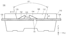
FIG. 1 is a transverse sectional view of the light emitting device according to the first embodiment, and FIG. 2 is a longitudinal sectional view of the light emitting device according to the first embodiment.
図1及び図2に示すように、発光装置100は、側面発光型又は上面発光型パッケージ
で実現されることができ、表示装置のライトユニット(light unit)や照明機
器などに多様に適用され得る。以下では、説明の便宜上、側面発光型LEDパッケージに
ついて説明する。
As shown in FIGS. 1 and 2, the
前記発光装置100は、キャビティ112を備えたパッケージ本体110、発光素子1
20、リードフレーム130を含む。
The
20, including a
前記パッケージ本体110は、樹脂材質を利用して形成され得る。前記パッケージ本体
110は、例えば、一定形状のプレス(Cu/Ni/Ag又はCu/Ag基板)金型にP
PA(高強化プラスチック)などの樹脂材質を利用して射出成形される。前記パッケージ
本体110は、他の例として、リードフレーム130を有する下部基板にキャビティが形
成された上部基板が積層される構造に形成されることができる。
The
Injection molding is performed using a resin material such as PA (highly reinforced plastic). As another example, the
ここで、発光装置100が側面発光型LEDパッケージで実現される場合、パッケージ
本体110の横方向は、パッケージ本体110の長さ方向Xであって長軸になり、パッケ
ージ本体110の縦方向は、パッケージ本体110の厚さ方向Yであって、短軸になる。
Here, when the
このようなパッケージ本体110の一側には、キャビティ112が形成され、前記キャ
ビティ112の下部には、パッケージ本体110の長さ方向Xに挿入されるリードフレー
ム130が形成される。
A
前記リードフレーム130は、複数が電気的にオープン(open)され、各リードフ
レーム130のリード電極132、134は、パッケージ本体110の外部に配置される
。ここで、キャビティ112の下部底面は、前記リードフレーム130の上面になり得る
。
A plurality of the
前記パッケージ本体110のキャビティ112は、一定深さ以下に形成される。前記キ
ャビティ112の深さd1は、キャビティ上段からリードフレーム130の上面までの距
離であり、例えば、250〜450μmに形成されることができる。
The
前記キャビティ112の側壁113、114のうち、少なくとも一側壁は、傾斜するよ
うに形成され得、実施形態では、全ての側壁が傾斜するように形成されるものと説明し、
これに限定しない。
Of the
It is not limited to this.
キャビティ112の側壁113、114は、キャビティ112の底面に垂直な軸Zを基
準に所定角度に傾斜するように形成される。前記Z軸は、キャビティ112の底面又はリ
ードフレーム130の上面に垂直した軸である。
The
図1に示すように、前記キャビティ112の長さ方向に位置した第1側壁113がなす
第1内部角度Θ1は、20〜80゜であり、前記キャビティ112の第1側壁113の角
度Θ11は、Z軸を基準に外側に10〜40゜傾斜するように形成される。図2に示すよ
うに、前記キャビティ112の厚さ方向に位置した第2側壁114がなす第2内部角度Θ
2は、20〜40゜であり、キャビティ112の第2側壁114の角度Θ21は、Z軸を
基準に外側に10〜20゜傾斜するように形成される。
As shown in FIG. 1, the first internal angle Θ1 formed by the
2 is 20 to 40 °, and the angle Θ21 of the
ここで、前記第1及び第2内部角度Θ1、Θ2は、同一又は異なるように形成できる。
また、第1側壁113及び第2側壁114の傾斜した角度Θ11、Θ21は、同一又は異
なるように形成されることができる。
Here, the first and second internal angles Θ1 and Θ2 may be the same or different.
In addition, the inclined angles Θ11 and Θ21 of the
このようなキャビティ112は、傾斜した側壁113、114により、下部直径より上
部直径が大きく形成される。また、前記キャビティ112の各側壁113、114には、
反射物質(例:Ag、Al)がコーティングされるか、又は反射板が付着され得る。前記
キャビティ112の外形状は、多角形形状に形成され得るが、これに限定しない。
The
A reflective material (eg, Ag, Al) can be coated or a reflector can be attached. The outer shape of the
前記キャビティ112には、1つ以上の半導体素子が備えられることができる。前記半
導体素子は、例えば、一つ以上の発光素子120、受光素子及び保護素子を選択的に含む
。
The
前記発光素子120は、例えば、GaAs系、AlGaAs系、GaN系、InGaN
系及びInGaAlP系などの化合物半導体材料を利用したLEDチップを一つ以上含む
。前記LEDチップは、例えば、青色LEDチップ、紫外線LEDチップ、赤色LEDチ
ップ、緑色LEDチップ、黄緑色(Yellow green)LEDチップを含み、P
N接合構造又はNPN接合構造、2つの電極が水平型又は垂直型に配置されるチップを含
むことができる。
The
One or more LED chips using a compound semiconductor material such as an InGaAlP system and an InGaAlP system are included. The LED chips include, for example, a blue LED chip, an ultraviolet LED chip, a red LED chip, a green LED chip, and a yellow green LED chip.
An N-junction structure or an NPN junction structure, and a chip in which two electrodes are arranged in a horizontal type or a vertical type can be included.
前記発光素子120は、少なくとも一つのリードフレーム130の上面に非導電性接着
剤で接着され、ワイヤー(wire)152、154又はフリップチップ(flip c
hip)方式によりリードフレーム130と接続される。
The
The
前記キャビティ112には、モールディング部材140が満たされる。前記モールディ
ング部材140は、透光性樹脂で満たされ、前記透光性樹脂には、蛍光体が添加されるこ
ともできる。前記モールディング部材140は、一液型(One Liquid typ
e)エポキシ、二液型(two liquid type)エポキシ、ハードタイプ(h
ard type)シリコーン、ソフトタイプ(soft type)シリコーンなどの
樹脂材料を利用することができる。ここで、前記モールディング部材140は、モールデ
ィング液又は添加物を使用目的、使用環境及び製品の特性に応じて選択的に使用すること
ができる。
The
e) Epoxy, two-liquid type epoxy, hard type (h
Resin materials such as ard type silicone and soft type silicone can be used. Here, the
このようなモールディング部材140の表面は、フラット(flat)形状、凹レンズ
形状又は凸レンズ形状のうちの何れかの形状に形成されることができ、前記モールディン
グ部材140上に凸レンズがさらに付着されることもできる。
The surface of the
このような発光装置100は、キャビティ112の底面と上面(発光ウィンドウ領域w
1)の広さは、従来のように等しく維持し、かつキャビティ112の深さd1を450μ
m以下に低く形成することによって、キャビティ112の側壁の傾斜角度が増加する。
Such a
The width of 1) is kept the same as before, and the depth d1 of the
By forming it lower than m, the inclination angle of the side wall of the
これにより、発光装置100は、既存より約20%以上の光効率が改善され、ライトユ
ニットの光源として適用される場合、既存より約30%以上の輝度改善効果がある。また
、キャビティの深さを最小化し、かつ側壁の傾斜角度を増加させることによって、側面型
発光ダイオードパッケージでの光度及び光量を増加させることができる。
As a result, the
図3は、図2の発光装置100を利用したライトユニット200の側断面図である。
FIG. 3 is a side sectional view of a
図3に示すように、ライトユニット200は、発光装置100、基板160、導光板1
62、反射部164を含む。
As shown in FIG. 3, the
62, including a
前記基板160上には、一つ以上の発光装置100が搭載される。前記導光板(LGP
:Light Guide Panel)162は、発光装置100の出射方向に配置さ
れ、入射される光を面光源として出射する。
One or more light emitting
: Light Guide Panel) 162 is arranged in the emission direction of the
前記導光板162の下部には、漏れる光を反射させるための反射部164が配置され、
前記導光板162の上部には、一枚以上の光学シート(図示せず)、例えば、拡散シート
、プリズムシートが配置されることができる。ここで、前記基板160は、フレキシブル
基板(FPCB)で実現されることができ、前記反射部164は、反射シートで実現され
ることができる。
Below the
One or more optical sheets (not shown) such as a diffusion sheet and a prism sheet may be disposed on the
前記発光装置100と導光板162との間隔d12は、組立て誤差により約200μm
程度のギャップが発生し得る。このとき、モールディング部材140の表面がフラット形
態であれば、モールディング部材140の表面と導光板162との間の間隔d13は、d
12となる。
The distance d12 between the light emitting
A degree of gap can occur. At this time, if the surface of the
12
又は、モールディング部材140の表面が凹レンズ形状であれば、モールディング部材
140の表面と導光板162との間の間隔は、約300μmとなる。このとき、キャビテ
ィ112の上段とモールディング部材140の表面(凹レンズ形状の高さ)との間隔は、
最大100μmになる。
Alternatively, if the surface of the
The maximum is 100 μm.
そして、キャビティ112の深さが最大450μmの場合、キャビティ112の底面か
ら導光板162との間の間隔d14は、最大650μm(=200μm+450μm)程
度になるので、発光素子120から導光板162までの距離は、従来より最大30%程度
減らすことができる。
When the depth of the
このように発光装置100の発光素子120から発生した光は、モールディング部材1
40を透過するか、キャビティ112の側壁114により反射してパッケージ本体110
の外部に放出される。前記パッケージ本体110から放出した光は、導光板162に入射
されることによって、導光板162から面光源として出力される。
Thus, the light generated from the
40 or reflected by the
Released to the outside. The light emitted from the
ここで、発光素子120からキャビティ112の上段までの間隔と、キャビティ112
の上段から導光板162の入光部までの間隔d12を最小化することによって、光損失区
間を減らして光抽出効果を極大化させることができる。また、導光板162と発光装置1
00との結合による光効率の減少を防止でき、導光板162でのガイド損失を減らし、輝
度の強度を改善することができる。
Here, the distance from the
By minimizing the distance d12 from the upper stage to the light incident part of the
The reduction of the light efficiency due to the coupling with 00 can be prevented, the guide loss in the
ここで、発光装置100から放出される光量は、発光素子120と導光板162との間
の間隔、モールディング部材140の表面形状、キャビティ112の内部角度などのパラ
メートルにより変わることができる。
Here, the amount of light emitted from the
また、上記の発光装置を利用して、携帯端末機などの液晶表示装置のバックライト光源
、照明分野などの面発光装置として構成できる。そして、ライトユニットのような面発光
装置において、発光素子から発生する光の損失区間を最小化し、光抽出効果を最大化でき
る。また、輝度の強度を改善できる。
In addition, the light emitting device described above can be used as a backlight light source of a liquid crystal display device such as a portable terminal or a surface light emitting device in the illumination field. In a surface light emitting device such as a light unit, the light loss generated from the light emitting element can be minimized and the light extraction effect can be maximized. In addition, the intensity of luminance can be improved.
図4は、実施形態に係る発光装置を介して出射された光の分布及び光量を測定するため
の図である。
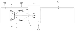
FIG. 4 is a diagram for measuring the distribution and amount of light emitted through the light emitting device according to the embodiment.
図4に示すように、発光素子120から出射される光は、モールディング部材140を
介して発光装置の前方に位置した受光部166及び導光板162に入射される。このとき
、前記受光部166は、前記導光板162に入射される光量(FLUX)を測定する。受
光部166は、5mm×0.6mmの面積で設置される。
As shown in FIG. 4, the light emitted from the
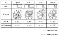
図5は、実施形態に係る発光装置のキャビティ深さ及びモールディング部材140の表
面形状を変更した場合、図4の受光部166に受光された光分布及び光量などを比較した
表である。ここで、試験条件としては、パッケージ本体は、PPA樹脂(Reflect
ance=90%適用)であり、モールディング部材の材質はシリコーン樹脂(refr
active index=1.42)であり、発光素子は容積が250μm×480μ
m×80μmであり、ピーク波長(peak wavelength)は455nmであ
り、半波高全幅値(FWHM)は、22nmのチップを適用する。
FIG. 5 is a table comparing the light distribution and the amount of light received by the
ance = 90% application) and the molding material is silicone resin (refr).
active index = 1.42), and the light emitting element has a volume of 250 μm × 480 μm.
A chip of m × 80 μm, a peak wavelength is 455 nm, and a half-wave height full width value (FWHM) is 22 nm.
ここで、配光分布は、発光装置の長軸方向(又は長さ方向)の配光分布(実線)と短縮
方向(又は厚さ方向)の配光分布(点線)により測定し、総光量は、発光装置から出射さ
れた光量であり、導光板(LGP)の入射光量は、前記受光部(図4の166)により実
際に受光された光量又は導光板に入射された光量である。
Here, the light distribution is measured by the light distribution (solid line) in the major axis direction (or length direction) and the light distribution (dotted line) in the shortening direction (or thickness direction) of the light emitting device. , The amount of light emitted from the light emitting device, and the amount of light incident on the light guide plate (LGP) is the amount of light actually received by the light receiving unit (166 in FIG. 4) or the amount of light incident on the light guide plate.
図5に示すように、第1パッケージタイプ区分1は、キャビティの深さが600μmで
あり、モールディング部材の表面がフラット形状である。このようなパッケージ構造にお
ける配光分布は、指向角度が相対的に狭く分布されており、総光量は、0.154lm、
導光板の入射光量は、0.124lmで測定される。
As shown in FIG. 5, the first package type section 1 has a cavity depth of 600 μm and a molding member having a flat surface. The light distribution in such a package structure is such that the directivity angle is relatively narrow and the total light amount is 0.154 lm,
The incident light quantity of the light guide plate is measured at 0.124 lm.
第2パッケージタイプ区分2は、キャビティの深さが600μmであり、モールディン
グ部材の表面が凹レンズ形状である。このようなパッケージ構造において配光分布は、狭
い指向角度で分布されており、総光量は、0.141lmであり、導光板の入射光量は、
0.102lmで測定される。
In the second package type section 2, the cavity depth is 600 μm, and the surface of the molding member has a concave lens shape. In such a package structure, the light distribution is distributed with a narrow directivity angle, the total light amount is 0.141 lm, and the incident light amount of the light guide plate is
Measured at 0.102 lm.
第3パッケージタイプ区分3は、キャビティの深さが300μmであり、モールディン
グ部材の表面がフラット形状である。このようなパッケージ構造において配光分布は、第
1及び第2パッケージタイプよりは指向特性が広く形成され、総光量は、0.207lm
であり、導光板の入射光量は、0.170lmで測定される。
In the third package type section 3, the cavity depth is 300 μm, and the surface of the molding member is flat. In such a package structure, the light distribution is formed with wider directivity than the first and second package types, and the total light amount is 0.207 lm.
The incident light quantity of the light guide plate is measured at 0.170 lm.
第4パッケージタイプ区分4は、キャビティの深さが300μmであり、モールディン
グ部材の表面が凹レンズ形状である。このようなパッケージ構造において配光分布は、第
1及び第2パッケージタイプよりは指向特性が広く形成され、総光量は、0.182lm
であり、導光板の入射光量は、0.158lmで測定される。
The fourth package type section 4 has a cavity depth of 300 μm, and the molding member surface has a concave lens shape. In such a package structure, the light distribution is formed with wider directivity than the first and second package types, and the total light amount is 0.182 lm.
The incident light quantity of the light guide plate is measured at 0.158 lm.
ここで、このようなパッケージタイプは、キャビティの深さ及びモールディング部材の
表面を変更したものである。実施形態の第3及び第4パッケージタイプ区分3、区分4と
第1及び第2パッケージタイプ区分1、区分2とを比較する場合、第3及び第4パッケー
ジタイプ区分3、区分4は、第1及び第2パッケージタイプ区分1、区分2よりは配光分
布の指向特性が広く、総光量及び導光板の入射光量が増加する。
Here, such a package type is obtained by changing the depth of the cavity and the surface of the molding member. When comparing the third and fourth package type category 3 and category 4 with the first and second package type category 1 and category 2, the third and fourth package type category 3 and category 4 are the first In addition, the directional characteristics of the light distribution are wider than those of the second package type category 1 and category 2, and the total light amount and the incident light amount of the light guide plate are increased.
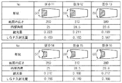
図6は、実施形態に係る発光装置において、キャビティの第2内部角度(Inside
angle)Θ7、Θ8、Θ9と前記キャビティの底面の広さとモールディング部材の
表面形状を異なるようにして、総光量と導光板の入射光量を測定した図である。ここで、
試験条件は、図5と同じ条件を適用する。
FIG. 6 illustrates a second internal angle (Inside) of the cavity in the light emitting device according to the embodiment.
angle) Θ7, Θ8, Θ9, and the width of the bottom surface of the cavity and the surface shape of the molding member are different, and the total light amount and the incident light amount of the light guide plate are measured. here,
The test conditions are the same as in FIG.
第11〜第13パッケージタイプ区分11、区分12、区分13は、モールディング部
材の表面がフラット形状であり、キャビティの内部角度Θ7、Θ8、Θ9及び底面の広さ
を変更して測定する。第14〜第16パッケージタイプ区分14、区分15、区分16は
、モールディング部材の表面が凹レンズ形状であり、キャビティの内部角度Θ7、Θ8、
Θ9及び底面の広さを変更して測定するようになる。ここで、第11〜第16パッケージ
タイプ区分11〜区分16のキャビティの深さは、全て同じ深さであり、実施形態で提供
する250〜450μmの範囲内にある。
In the 11th to 13th
Measurement is performed by changing Θ9 and the width of the bottom surface. Here, the depths of the cavities of the 11th to 16th
前記第11パッケージタイプ区分11及び第14パッケージタイプ区分14は、キャビ
ティの内部角度Θ7が25゜であり、キャビティの底面の広さは350μmである。第1
2パッケージタイプ区分12及び第15パッケージタイプ区分15は、キャビティの内部
角度Θ8が28.5゜であり、キャビティの底面の広さは、310μmである。第13パ
ッケージタイプ区分13及び第16パッケージタイプ区分16は、キャビティの内部角度
Θ9が20.6゜であり、キャビティの底面の広さは、380μmである。ここで、前記
キャビティの内部角度Θ7、Θ8、Θ9は、該当キャビティの底面の広さと反比例する。
In the eleventh
In the second
総光量を見れば、第11パッケージタイプ区分11は0.233lm、第12パッケー
ジタイプ区分12は0.211lm、第13パッケージタイプ区分13は0.199lm
、第14パッケージタイプ区分14は0.212lm、第15パッケージタイプ区分15
は0.188lm、そして第16パッケージタイプ区分16は0.212lmで測定され
る。
Looking at the total light quantity, the eleventh
14th package type section 14 is 0.212 lm, 15th package type section 15
0.188 lm, and the 16th package type section 16 is measured at 0.212 lm.
導光板LGPの入射光量を見れば、第11パッケージタイプ区分11は0.169lm
、第12パッケージタイプ区分12は0.160lm、第13パッケージタイプ区分13
は0.147lm、第14パッケージタイプ区分14は0.166lm、第15パッケー
ジタイプ区分15は0.149lm、第16パッケージタイプ区分16は0.166lm
である。
Looking at the amount of light incident on the light guide plate LGP, the eleventh
The 12th
0.147lm, 14th package type section 14 is 0.166lm, 15th package type section 15 is 0.149lm, 16th package type section 16 is 0.166lm
It is.
ここで、前記第11〜第16パッケージタイプ区分11〜区分16は、図5の第1及び
第2パッケージタイプ区分1、区分2よりは光量特性が全て高く現れている。また、第1
1パッケージタイプ区分11は、総光量や導光板の入射光量が他のパッケージタイプに比
べて最も高く現れている。すなわち、同一深さのキャビティでは、キャビティの内部角度
と底面の広さに応じて、総光量や導光板の入射光量に差があるようになる。
Here, the 11th to 16th
In the one
このような発光装置では、キャビティの深さを最小化し、かつ側壁の傾斜角度を増加さ
せることによって、側面型発光ダイオードパッケージでの光度及び光量を増加させること
ができる。
In such a light emitting device, it is possible to increase the luminous intensity and the amount of light in the side surface type light emitting diode package by minimizing the depth of the cavity and increasing the inclination angle of the side wall.
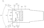
図7は、第2の実施形態であって、発光装置101の縦断面図である。
FIG. 7 is a longitudinal sectional view of the
図7に示すように、パッケージ本体110は、キャビティ112の側壁114が2回以
上折り曲げられた構造である。前記キャビティ112の側壁114は、下部側壁115及
び上部側壁116を含み、下部側壁115の第3内部角度Θ3は、上部側壁116の第4
内部角度Θ4より大きく形成される。前記キャビティ112の深さ(=d5+d6)は、
450μm以下に形成され、上部側壁116の高さd6は、下部側壁115の高さd5よ
り高く形成される。
As shown in FIG. 7, the
It is formed larger than the internal angle Θ4. The depth of the cavity 112 (= d5 + d6) is
The height d6 of the
例えば、キャビティ112の下部側壁115は、キャビティ112の底面から70〜2
50μm地点までであり、第3内部角度Θ3は、30〜50゜に傾斜する。上部側壁11
6は、上部側壁116が始まる地点からキャビティ上段までの高さd6であって、200
〜380μmに形成され、上部側壁の第4内部角度Θ4は、約0〜20゜程度に傾斜する
。ここで、下部側壁115の第3内部角度Θ3内で両側壁115の角度Θ31、Θ32は
、互いに同一又は異なることができる。また、上部側壁116の角度Θ4内で両側壁の角
度Θ41、Θ42は、互いに同一又は異なることができる。
For example, the
The third internal angle Θ3 is inclined at 30 to 50 °.
6 is a height d6 from the point where the
The fourth inner angle Θ4 of the upper side wall is inclined to about 0 to 20 °. Here, the angles Θ31 and Θ32 of the
前記キャビティ112の下部側壁115は、発光素子120から発生した光が最大限上
側に反射できる高さ、例えば、発光素子120の高さ(例、70〜130μm)より高く
形成されることができる。このとき、キャビティ112の下部側壁115の角度Θ3によ
って発光素子120と下部側壁115との間の距離d7がより遠ざかるようになることに
よって、発光素子120から発生する熱又は光により、射出樹脂が変色(すなわち、側壁
の変色)することを防止できる。
The
また、キャビティ112の側壁114に対した傾斜角度を調節することによって、他の
キャビティに比べて光効率を最大限高めることができる。
Further, by adjusting the inclination angle of the
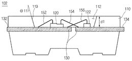
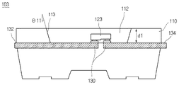
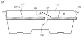
図8〜図10は、第1の実施形態に係る発光装置において、半導体素子の多様な実装例
を示した断面図である。
8 to 10 are cross-sectional views showing various mounting examples of semiconductor elements in the light emitting device according to the first embodiment.
図8に示すように、発光装置102には、一つ以上の発光素子120と保護素子122
が搭載される。パッケージ本体110のキャビティ112には、一つ以上の発光素子12
0及び保護素子122がリードフレーム130にチップ形態で実装される。前記発光素子
120は、一側のリードフレーム130に接着され、ワイヤー152、154により接続
される。前記保護素子122は、他側のリードフレーム130に接着され、他のリードフ
レームとワイヤー156により接続される。又は、キャビティ内でワイヤーの高さを減ら
すために、半導体素子をリバース(reverse)方式により搭載することもできる。
As shown in FIG. 8, the
Is installed. In the
0 and the protection element 122 are mounted on the
図9に示すように、発光装置103は、一つ以上の発光素子123がフリップチップ方
式により搭載される。このために、発光素子123の両電極が2つのリードフレーム13
0にソルダーバンプを利用してフリップチップ方式により接続される。
As shown in FIG. 9, in the
0 is connected by a flip chip method using a solder bump.
図10に示すように、発光装置104は、一つ以上の垂直型発光素子124を含む。こ
のために、垂直型発光素子124の第1電極は、一側のリードフレーム130に導電性接
着剤により接着され、垂直型発光素子124の第2電極は、他側のリードフレーム130
にワイヤー154により接続される。
As shown in FIG. 10, the
Are connected by
そして、図8〜図10のパッケージ本体110の外部には、二つのリードフレーム13
0のリード電極132、134が形成される。
8 to 10, two lead frames 13 are provided outside the
Zero
図11は、実施形態に係る発光装置のパッケージ構造を示した図であって、半導体素子
が搭載される前の図である。図11(a)は、パッケージ本体の横断面図であり、図11
(b)は、パッケージ本体の正面図であり、図11(c)は、パッケージ本体の底面図で
ある。
FIG. 11 is a view showing a package structure of the light emitting device according to the embodiment, and is a view before a semiconductor element is mounted. FIG. 11A is a cross-sectional view of the package body, and FIG.
(B) is a front view of a package main body, FIG.11 (c) is a bottom view of a package main body.
図11の(a)に示すように、パッケージ本体110のキャビティ112の下部に位置
したリードフレーム130は、キャビティ112の底面に対応する高さd1でベースライ
ンを構成する。
As shown in FIG. 11A, the
図11の(b)、(c)に示すように、リードフレーム130の第1及び第2リード電
極132、134は、パッケージ本体110の外部から側面方向へ1次フォーミング(f
orming)され、パッケージ本体110の底面の両側に形成された溝118に2次フ
ォーミングされる。前記第1及び第2リード電極132、134の両端133、135は
、パッケージ本体110の底面の両側に配置されて、基板上に表面実装技術(SMT)に
より実装され得る。
As shown in FIGS. 11B and 11C, the first and second
and secondarily formed in
上述した本発明の好ましい実施の形態は、例示の目的のために開示されたものであり、
本発明の属する技術の分野における通常の知識を有する者であれば、本発明の技術的思想
を逸脱しない範囲内で、様々な置換、変形、及び変更が可能であり、このような置換、変
更などは、特許請求の範囲に属するものである。
The preferred embodiments of the invention described above have been disclosed for purposes of illustration,
Anyone who has ordinary knowledge in the technical field to which the present invention pertains can make various substitutions, modifications, and changes without departing from the technical idea of the present invention. And the like belong to the scope of the claims.
100 発光装置、 110 パッケージ本体、 112 キャビティ、 113、1
14 側壁、 120 発光素子、 130 リードフレーム、 132、134 リー
ド電極、 140 モールディング部材、 152 154,ワイヤー。
100 light emitting device, 110 package body, 112 cavity, 113, 1
14 side wall, 120 light emitting element, 130 lead frame, 132, 134 lead electrode, 140 molding member, 152 154, wire.
Claims (12)
前記キャビティの前記底面を形成する実装部分と、前記実装部分から前記パッケージ本体の外に延長された平坦部分を有するリードフレーム、前記リードフレームの前記実装部分の上に配置された発光素子、を含み、
前記キャビティの前記第1内壁と前記キャビティの前記第2内壁との間の第1角度は、前記キャビティの前記第3内壁と前記キャビティの前記第4内壁との間の第2角度と異なり、
前記パッケージの前記前面から前記キャビティの前記底面までの距離は、450μmより小さく、
前記キャビティの前記底面に対する前記キャビティの前記第1内壁の傾斜角は、前記キャビティの前記底面に対する前記キャビティの前記第3内壁の傾斜角と異なり、
前記パッケージ本体は、前記パッケージ本体の横面から前記前面と前記パッケージ本体の前記後面との間に延長された側面を含み、
前記側面は、前記キャビティの近くに前記パッケージ本体の前記前面に垂直な方向に配置された第1側面と、前記第1側面から延長された第2側面を含み、
前記パッケージ本体の前記第2側面は、前記パッケージ本体の前記前面に垂直な軸に対して傾斜するように配置され、
前記パッケージ本体の前記前面に対する前記第1側面の傾斜角は、前記パッケージ本体の前記前面に対する前記第2側面の傾斜角と異なる、発光装置。 A package body including a resin and a cavity, the cavity including a bottom surface and an inner wall surrounding the bottom surface, the package body serving as an upper surface of the cavity and having an opening; and the package with respect to the front surface A rear surface disposed on an opposite surface of the main body, the rear surface including a recess recessed in the front surface direction, the inner wall includes a first inner wall, a second inner wall facing the first inner wall, a third inner wall, Including a fourth inner wall facing the third inner wall, wherein at least one of the third inner wall and the fourth inner wall includes a lower sidewall and an upper sidewall;
A mounting portion forming the bottom surface of the cavity; a lead frame having a flat portion extending from the mounting portion to the outside of the package body; and a light emitting device disposed on the mounting portion of the lead frame. ,
A first angle between the first inner wall of the cavity and the second inner wall of the cavity is different from a second angle between the third inner wall of the cavity and the fourth inner wall of the cavity;
The distance from the front surface of the package to the bottom surface of the cavity is less than 450 μm,
The inclination angle of the first inner wall of the cavity with respect to the bottom surface of the cavity is different from the inclination angle of the third inner wall of the cavity with respect to the bottom surface of the cavity,
The package body includes a side surface extending from a lateral surface of the package body between the front surface and the rear surface of the package body,
The side surface includes a first side surface disposed in a direction perpendicular to the front surface of the package body near the cavity, and a second side surface extending from the first side surface,
The second side surface of the package body is disposed to be inclined with respect to an axis perpendicular to the front surface of the package body;
The light emitting device, wherein an inclination angle of the first side surface with respect to the front surface of the package body is different from an inclination angle of the second side surface with respect to the front surface of the package body.
前記第3内壁の前記下部側壁と前記第4内壁の前記下部側壁との間の角度は、前記第3内壁の前記上部側壁と前記第4内壁の前記上部側壁との間の角度より大きい、請求項1に記載の発光装置。 Each of the third inner wall and the fourth inner wall includes a lower sidewall and an upper sidewall,
The angle between the lower side wall of the third inner wall and the lower side wall of the fourth inner wall is greater than an angle between the upper side wall of the third inner wall and the upper side wall of the fourth inner wall. Item 4. The light emitting device according to Item 1.
前記キャビティの前記第3内壁の前記下部側壁の傾斜角が、前記キャビティの前記第4内壁の前記下部側壁の傾斜角と異なるか、前記キャビティの前記第3内壁の前記上部側壁の傾斜角が、前記キャビティの前記第4内壁の前記上部側壁の傾斜角と異なる、請求項1に記載の発光装置。 The third inner wall of the cavity and the fourth inner wall of the cavity each include a lower sidewall and an upper sidewall;
The inclination angle of the lower side wall of the third inner wall of the cavity is different from the inclination angle of the lower side wall of the fourth inner wall of the cavity, or the inclination angle of the upper side wall of the third inner wall of the cavity is The light emitting device according to claim 1, wherein the light emitting device is different from an inclination angle of the upper side wall of the fourth inner wall of the cavity.
前記キャビティの前記第3内壁の前記下部側壁の傾斜角が、前記キャビティの前記第4内壁の前記下部側壁の傾斜角と異なり、
前記キャビティの前記第3内壁の前記上部側壁の傾斜角が、前記キャビティの前記第4内壁の前記上部側壁の傾斜角と異なる、請求項1に記載の発光装置。 The third inner wall of the cavity and the fourth inner wall of the cavity each include a lower sidewall and an upper sidewall,
The inclination angle of the lower side wall of the third inner wall of the cavity is different from the inclination angle of the lower side wall of the fourth inner wall of the cavity,
The light emitting device according to claim 1, wherein an inclination angle of the upper side wall of the third inner wall of the cavity is different from an inclination angle of the upper side wall of the fourth inner wall of the cavity.
Applications Claiming Priority (2)
| Application Number | Priority Date | Filing Date | Title |
|---|---|---|---|
| KR1020060042199A KR100820529B1 (en) | 2006-05-11 | 2006-05-11 | Light emitting device and manufacturing method thereof, surface light emitting device |
| KR10-2006-0042199 | 2006-05-11 |
Related Parent Applications (1)
| Application Number | Title | Priority Date | Filing Date |
|---|---|---|---|
| JP2016094429A Division JP6195956B2 (en) | 2006-05-11 | 2016-05-10 | Side-emitting type light emitting device |
Related Child Applications (1)
| Application Number | Title | Priority Date | Filing Date |
|---|---|---|---|
| JP2018242218A Division JP6681970B2 (en) | 2006-05-11 | 2018-12-26 | Side-emitting light-emitting device |
Publications (2)
| Publication Number | Publication Date |
|---|---|
| JP2017201729A true JP2017201729A (en) | 2017-11-09 |
| JP6462065B2 JP6462065B2 (en) | 2019-01-30 |
Family
ID=38684294
Family Applications (9)
| Application Number | Title | Priority Date | Filing Date |
|---|---|---|---|
| JP2007126415A Active JP5242945B2 (en) | 2006-05-11 | 2007-05-11 | LIGHT EMITTING DEVICE AND LIGHT EMITTING DEVICE MANUFACTURING METHOD |
| JP2012039856A Active JP5225480B2 (en) | 2006-05-11 | 2012-02-27 | LIGHT EMITTING DEVICE AND LIGHT EMITTING DEVICE MANUFACTURING METHOD |
| JP2012039857A Expired - Fee Related JP5236823B2 (en) | 2006-05-11 | 2012-02-27 | LIGHT EMITTING DEVICE AND LIGHT EMITTING DEVICE MANUFACTURING METHOD |
| JP2012001044U Expired - Lifetime JP3175535U (en) | 2006-05-11 | 2012-02-27 | Light emitting device and method for manufacturing light emitting device |
| JP2013078354A Expired - Fee Related JP5563693B2 (en) | 2006-05-11 | 2013-04-04 | LIGHT EMITTING DEVICE AND LIGHT EMITTING DEVICE MANUFACTURING METHOD |
| JP2014121535A Expired - Fee Related JP5936650B2 (en) | 2006-05-11 | 2014-06-12 | LIGHT EMITTING DEVICE AND LIGHT EMITTING DEVICE MANUFACTURING METHOD |
| JP2016094429A Expired - Fee Related JP6195956B2 (en) | 2006-05-11 | 2016-05-10 | Side-emitting type light emitting device |
| JP2017157215A Expired - Fee Related JP6462065B2 (en) | 2006-05-11 | 2017-08-16 | Side-emitting type light emitting device |
| JP2018242218A Expired - Fee Related JP6681970B2 (en) | 2006-05-11 | 2018-12-26 | Side-emitting light-emitting device |
Family Applications Before (7)
| Application Number | Title | Priority Date | Filing Date |
|---|---|---|---|
| JP2007126415A Active JP5242945B2 (en) | 2006-05-11 | 2007-05-11 | LIGHT EMITTING DEVICE AND LIGHT EMITTING DEVICE MANUFACTURING METHOD |
| JP2012039856A Active JP5225480B2 (en) | 2006-05-11 | 2012-02-27 | LIGHT EMITTING DEVICE AND LIGHT EMITTING DEVICE MANUFACTURING METHOD |
| JP2012039857A Expired - Fee Related JP5236823B2 (en) | 2006-05-11 | 2012-02-27 | LIGHT EMITTING DEVICE AND LIGHT EMITTING DEVICE MANUFACTURING METHOD |
| JP2012001044U Expired - Lifetime JP3175535U (en) | 2006-05-11 | 2012-02-27 | Light emitting device and method for manufacturing light emitting device |
| JP2013078354A Expired - Fee Related JP5563693B2 (en) | 2006-05-11 | 2013-04-04 | LIGHT EMITTING DEVICE AND LIGHT EMITTING DEVICE MANUFACTURING METHOD |
| JP2014121535A Expired - Fee Related JP5936650B2 (en) | 2006-05-11 | 2014-06-12 | LIGHT EMITTING DEVICE AND LIGHT EMITTING DEVICE MANUFACTURING METHOD |
| JP2016094429A Expired - Fee Related JP6195956B2 (en) | 2006-05-11 | 2016-05-10 | Side-emitting type light emitting device |
Family Applications After (1)
| Application Number | Title | Priority Date | Filing Date |
|---|---|---|---|
| JP2018242218A Expired - Fee Related JP6681970B2 (en) | 2006-05-11 | 2018-12-26 | Side-emitting light-emitting device |
Country Status (3)
| Country | Link |
|---|---|
| US (5) | US8680545B2 (en) |
| JP (9) | JP5242945B2 (en) |
| KR (1) | KR100820529B1 (en) |
Families Citing this family (25)
| Publication number | Priority date | Publication date | Assignee | Title |
|---|---|---|---|---|
| JP2901278B2 (en) | 1989-09-27 | 1999-06-07 | 新日本製鐵株式会社 | Water treatment filter and method for producing the same |
| KR100820529B1 (en) | 2006-05-11 | 2008-04-08 | 엘지이노텍 주식회사 | Light emitting device and manufacturing method thereof, surface light emitting device |
| KR20080065451A (en) * | 2007-01-09 | 2008-07-14 | 삼성전기주식회사 | LED Package |
| JP5084365B2 (en) * | 2007-06-21 | 2012-11-28 | シャープ株式会社 | LED light emitting device and liquid crystal backlight device using the same as light source |
| JP5416975B2 (en) | 2008-03-11 | 2014-02-12 | ローム株式会社 | Semiconductor light emitting device |
| KR101028852B1 (en) | 2008-03-26 | 2011-04-12 | 서울반도체 주식회사 | Side view LED package and backlight module including the same |
| KR20100003320A (en) * | 2008-06-24 | 2010-01-08 | 엘지이노텍 주식회사 | Light emitting diode package |
| KR101093249B1 (en) * | 2008-09-30 | 2011-12-14 | 서울반도체 주식회사 | Light emitting element |
| KR101509760B1 (en) * | 2008-10-16 | 2015-04-08 | 엘지이노텍 주식회사 | Light emitting diode package and fabrication method thereof, light emitting apparatus having the same |
| EP2448023B1 (en) | 2009-06-22 | 2016-08-31 | Nichia Corporation | Light-emitting device |
| KR101118988B1 (en) * | 2010-03-11 | 2012-03-12 | (주)티에스티아이테크 | Back light unit and liquid crystal display device using the same |
| JP5777879B2 (en) * | 2010-12-27 | 2015-09-09 | ローム株式会社 | Light emitting device, light emitting device unit, and light emitting device package |
| KR101714073B1 (en) * | 2011-08-10 | 2017-03-08 | 엘지이노텍 주식회사 | The light emitting device package and the light emitting system |
| JP2013179271A (en) | 2012-01-31 | 2013-09-09 | Rohm Co Ltd | Light emitting device and manufacturing method of the same |
| KR20130118552A (en) * | 2012-04-20 | 2013-10-30 | 엘지이노텍 주식회사 | Light emitting device package and light emitting apparatus having the same |
| KR101949387B1 (en) * | 2012-09-12 | 2019-02-19 | 엘지디스플레이 주식회사 | LED package and method of manufacturing the same and liquid crystal display device including LED package |
| KR102076243B1 (en) * | 2013-09-04 | 2020-02-12 | 엘지이노텍 주식회사 | A light emitting device package |
| JP6414427B2 (en) * | 2013-10-03 | 2018-10-31 | 日亜化学工業株式会社 | Light emitting device mounting structure |
| WO2016035508A1 (en) * | 2014-09-01 | 2016-03-10 | シャープ株式会社 | Light emitting device |
| JP6730017B2 (en) * | 2014-11-10 | 2020-07-29 | エルジー イノテック カンパニー リミテッド | Light emitting device package and lighting system including the same |
| JP6651699B2 (en) * | 2015-02-27 | 2020-02-19 | 日亜化学工業株式会社 | Manufacturing method of side emission type light emitting device |
| DE102015105137A1 (en) * | 2015-04-02 | 2016-10-06 | Osram Opto Semiconductors Gmbh | Optoelectronic component |
| JP6793139B2 (en) * | 2018-01-25 | 2020-12-02 | 日機装株式会社 | Semiconductor light emitting device |
| KR102490162B1 (en) * | 2018-02-14 | 2023-01-19 | 쑤저우 레킨 세미컨덕터 컴퍼니 리미티드 | Light emitting device and light emitting device package including the same |
| KR101970938B1 (en) * | 2019-02-11 | 2019-04-19 | 진재언 | Light emitting device package having a controlled beam angle and light emitting apparatus using the same |
Citations (13)
| Publication number | Priority date | Publication date | Assignee | Title |
|---|---|---|---|---|
| JPH0497366U (en) * | 1991-01-17 | 1992-08-24 | ||
| JPH11121809A (en) * | 1997-10-16 | 1999-04-30 | Matsushita Electron Corp | Semiconductor light emitting device |
| JP2000012894A (en) * | 1998-06-17 | 2000-01-14 | Matsushita Electron Corp | Semiconductor light emitting device |
| JP2000269551A (en) * | 1999-03-18 | 2000-09-29 | Rohm Co Ltd | Chip type light emitting device |
| JP2004228550A (en) * | 2002-11-25 | 2004-08-12 | Kyocera Corp | Light emitting element storage package and light emitting device |
| JP2004311917A (en) * | 2003-02-19 | 2004-11-04 | Kyocera Corp | Light emitting element storage package and light emitting device |
| JP2005109382A (en) * | 2003-10-02 | 2005-04-21 | Citizen Electronics Co Ltd | Light emitting diode |
| JP2005252168A (en) * | 2004-03-08 | 2005-09-15 | Nichia Chem Ind Ltd | Surface mount light emitting device |
| JP2006019676A (en) * | 2003-10-15 | 2006-01-19 | Nichia Chem Ind Ltd | Heat sink and semiconductor device provided with heat sink |
| JP2006019313A (en) * | 2004-06-30 | 2006-01-19 | Sanyo Electric Co Ltd | LED display housing, LED display, and LED display connecting member |
| US20060027826A1 (en) * | 2004-08-09 | 2006-02-09 | Joel Lee Goodrich | Light emitting diode package |
| JP2006058327A (en) * | 2004-08-17 | 2006-03-02 | Sony Corp | Optical waveguide device and optical coupling device |
| JP2007150315A (en) * | 2005-11-25 | 2007-06-14 | Samsung Electro Mech Co Ltd | Side-emitting LED package |
Family Cites Families (48)
| Publication number | Priority date | Publication date | Assignee | Title |
|---|---|---|---|---|
| JPH01168079A (en) | 1987-12-23 | 1989-07-03 | Ibiden Co Ltd | Led mounting board |
| US6274890B1 (en) * | 1997-01-15 | 2001-08-14 | Kabushiki Kaisha Toshiba | Semiconductor light emitting device and its manufacturing method |
| JP3421621B2 (en) | 1999-12-24 | 2003-06-30 | 三洋電機株式会社 | Surface light source device |
| JP2002009349A (en) | 2000-06-26 | 2002-01-11 | Koha Co Ltd | LED surface light emitting device and method of manufacturing the same |
| JP2002033520A (en) | 2000-07-14 | 2002-01-31 | Toshiba Electronic Engineering Corp | Semiconductor light emitting device |
| JP2002093202A (en) * | 2000-09-13 | 2002-03-29 | Ryoden Trading Co Ltd | Manufacturing method of surface emitting backlight device and surface emitting backlight device |
| US6547416B2 (en) * | 2000-12-21 | 2003-04-15 | Koninklijke Philips Electronics N.V. | Faceted multi-chip package to provide a beam of uniform white light from multiple monochrome LEDs |
| JP2002217459A (en) | 2001-01-16 | 2002-08-02 | Stanley Electric Co Ltd | Light emitting diode and backlight device for liquid crystal display using light emitting diode as light source |
| JP2002299698A (en) * | 2001-03-30 | 2002-10-11 | Sumitomo Electric Ind Ltd | Light emitting device |
| EP1416219B1 (en) * | 2001-08-09 | 2016-06-22 | Everlight Electronics Co., Ltd | Led illuminator and card type led illuminating light source |
| JP2003234008A (en) | 2002-02-06 | 2003-08-22 | Nichia Chem Ind Ltd | Surface emitting device |
| JP2003347600A (en) | 2002-05-28 | 2003-12-05 | Matsushita Electric Works Ltd | LED mounting board |
| JP2004053807A (en) | 2002-07-18 | 2004-02-19 | Renesas Technology Corp | Mask manufacturer selection method |
| TWI292961B (en) * | 2002-09-05 | 2008-01-21 | Nichia Corp | Semiconductor device and an optical device using the semiconductor device |
| JP4081394B2 (en) | 2003-03-18 | 2008-04-23 | 京セラ株式会社 | Light emitting element storage package and light emitting device |
| KR20040087566A (en) | 2003-04-08 | 2004-10-14 | 엘지전자 주식회사 | Vibration mode setting method for mobile communication device |
| JP4070208B2 (en) | 2003-04-21 | 2008-04-02 | 京セラ株式会社 | Light emitting element storage package and light emitting device |
| JP2004327504A (en) | 2003-04-21 | 2004-11-18 | Kyocera Corp | Light emitting element storage package and light emitting device |
| JP4645071B2 (en) * | 2003-06-20 | 2011-03-09 | 日亜化学工業株式会社 | Package molded body and semiconductor device using the same |
| JP2005078937A (en) | 2003-08-29 | 2005-03-24 | Ichikoh Ind Ltd | Thin light emitting device |
| US20050133808A1 (en) * | 2003-09-11 | 2005-06-23 | Kyocera Corporation | Package for housing light-emitting element, light-emitting apparatus and illumination apparatus |
| TWI245436B (en) * | 2003-10-30 | 2005-12-11 | Kyocera Corp | Package for housing light-emitting element, light-emitting apparatus and illumination apparatus |
| JP2005136349A (en) | 2003-10-31 | 2005-05-26 | Toyoda Gosei Co Ltd | Light emitting device and reflection mirror thereof |
| JP3906199B2 (en) | 2003-11-27 | 2007-04-18 | 京セラ株式会社 | Light emitting device |
| JP2005191530A (en) * | 2003-12-03 | 2005-07-14 | Sumitomo Electric Ind Ltd | Light emitting device |
| JP4654670B2 (en) * | 2003-12-16 | 2011-03-23 | 日亜化学工業株式会社 | Light emitting device and manufacturing method thereof |
| JP4309242B2 (en) * | 2003-12-19 | 2009-08-05 | Necライティング株式会社 | Red phosphor material, white light emitting diode using red phosphor material, and lighting device using white light emitting diode |
| JP4325412B2 (en) | 2004-01-21 | 2009-09-02 | 日亜化学工業株式会社 | LIGHT EMITTING DEVICE AND LIGHT EMITTING DEVICE MANUFACTURING METHOD |
| KR100583159B1 (en) * | 2004-02-16 | 2006-05-23 | 엘지이노텍 주식회사 | Light emitting diode package |
| US7009285B2 (en) * | 2004-03-19 | 2006-03-07 | Lite-On Technology Corporation | Optoelectronic semiconductor component |
| JP2005285874A (en) | 2004-03-26 | 2005-10-13 | Kyocera Corp | Light emitting element storage package, light emitting device, and lighting device |
| JP4544619B2 (en) | 2004-06-08 | 2010-09-15 | ローム株式会社 | Light emitting diode lamp |
| KR20060000544A (en) * | 2004-06-29 | 2006-01-06 | 삼성전자주식회사 | Backlight for display device, Light source for display device, Light emitting diode for light source |
| JP4521227B2 (en) * | 2004-07-14 | 2010-08-11 | 株式会社東芝 | Method for producing phosphor containing nitrogen |
| KR100674827B1 (en) * | 2004-07-28 | 2007-01-25 | 삼성전기주식회사 | LED package for backlight unit |
| JP5081370B2 (en) | 2004-08-31 | 2012-11-28 | 日亜化学工業株式会社 | Light emitting device |
| JP2006100575A (en) | 2004-09-29 | 2006-04-13 | Hitachi Cable Precision Co Ltd | Surface mount light emitting device |
| US7385227B2 (en) * | 2005-04-12 | 2008-06-10 | Avago Technologies Ecbu Ip Pte Ltd | Compact light emitting device package with enhanced heat dissipation and method for making the package |
| KR100650191B1 (en) * | 2005-05-31 | 2006-11-27 | 삼성전기주식회사 | High brightness LEDs with built-in protection against electrostatic discharge shock |
| JP2006351773A (en) | 2005-06-15 | 2006-12-28 | Rohm Co Ltd | Semiconductor light emitting device |
| US7279722B2 (en) * | 2005-10-21 | 2007-10-09 | Avago Technologies Ecbu Ip (Singapore) Pte Ltd | Light emitting device with adjustable reflector cup |
| US7943946B2 (en) * | 2005-11-21 | 2011-05-17 | Sharp Kabushiki Kaisha | Light emitting device |
| KR100820529B1 (en) * | 2006-05-11 | 2008-04-08 | 엘지이노텍 주식회사 | Light emitting device and manufacturing method thereof, surface light emitting device |
| JP4729441B2 (en) * | 2006-06-09 | 2011-07-20 | スタンレー電気株式会社 | Vehicle lighting |
| JP2008016565A (en) * | 2006-07-04 | 2008-01-24 | Shinko Electric Ind Co Ltd | LIGHT EMITTING ELEMENT CONTAINER, MANUFACTURING METHOD THEREOF, AND LIGHT EMITTING DEVICE |
| US7968900B2 (en) * | 2007-01-19 | 2011-06-28 | Cree, Inc. | High performance LED package |
| US8030674B2 (en) * | 2008-04-28 | 2011-10-04 | Lextar Electronics Corp. | Light-emitting diode package with roughened surface portions of the lead-frame |
| JP4530082B2 (en) * | 2008-07-31 | 2010-08-25 | エプソンイメージングデバイス株式会社 | Backlight unit, electro-optical device and electronic apparatus |
-
2006
- 2006-05-11 KR KR1020060042199A patent/KR100820529B1/en not_active Expired - Lifetime
-
2007
- 2007-05-10 US US11/746,783 patent/US8680545B2/en not_active Expired - Fee Related
- 2007-05-11 JP JP2007126415A patent/JP5242945B2/en active Active
-
2012
- 2012-02-27 JP JP2012039856A patent/JP5225480B2/en active Active
- 2012-02-27 JP JP2012039857A patent/JP5236823B2/en not_active Expired - Fee Related
- 2012-02-27 JP JP2012001044U patent/JP3175535U/en not_active Expired - Lifetime
-
2013
- 2013-04-04 JP JP2013078354A patent/JP5563693B2/en not_active Expired - Fee Related
- 2013-07-09 US US13/937,899 patent/US9564556B2/en not_active Expired - Fee Related
-
2014
- 2014-06-12 JP JP2014121535A patent/JP5936650B2/en not_active Expired - Fee Related
-
2016
- 2016-05-10 JP JP2016094429A patent/JP6195956B2/en not_active Expired - Fee Related
- 2016-12-20 US US15/385,355 patent/US9882095B2/en not_active Expired - Fee Related
-
2017
- 2017-08-16 JP JP2017157215A patent/JP6462065B2/en not_active Expired - Fee Related
- 2017-12-13 US US15/840,967 patent/US10243112B2/en active Active
-
2018
- 2018-12-26 JP JP2018242218A patent/JP6681970B2/en not_active Expired - Fee Related
-
2019
- 2019-02-07 US US16/269,935 patent/US10580943B2/en active Active
Patent Citations (13)
| Publication number | Priority date | Publication date | Assignee | Title |
|---|---|---|---|---|
| JPH0497366U (en) * | 1991-01-17 | 1992-08-24 | ||
| JPH11121809A (en) * | 1997-10-16 | 1999-04-30 | Matsushita Electron Corp | Semiconductor light emitting device |
| JP2000012894A (en) * | 1998-06-17 | 2000-01-14 | Matsushita Electron Corp | Semiconductor light emitting device |
| JP2000269551A (en) * | 1999-03-18 | 2000-09-29 | Rohm Co Ltd | Chip type light emitting device |
| JP2004228550A (en) * | 2002-11-25 | 2004-08-12 | Kyocera Corp | Light emitting element storage package and light emitting device |
| JP2004311917A (en) * | 2003-02-19 | 2004-11-04 | Kyocera Corp | Light emitting element storage package and light emitting device |
| JP2005109382A (en) * | 2003-10-02 | 2005-04-21 | Citizen Electronics Co Ltd | Light emitting diode |
| JP2006019676A (en) * | 2003-10-15 | 2006-01-19 | Nichia Chem Ind Ltd | Heat sink and semiconductor device provided with heat sink |
| JP2005252168A (en) * | 2004-03-08 | 2005-09-15 | Nichia Chem Ind Ltd | Surface mount light emitting device |
| JP2006019313A (en) * | 2004-06-30 | 2006-01-19 | Sanyo Electric Co Ltd | LED display housing, LED display, and LED display connecting member |
| US20060027826A1 (en) * | 2004-08-09 | 2006-02-09 | Joel Lee Goodrich | Light emitting diode package |
| JP2006058327A (en) * | 2004-08-17 | 2006-03-02 | Sony Corp | Optical waveguide device and optical coupling device |
| JP2007150315A (en) * | 2005-11-25 | 2007-06-14 | Samsung Electro Mech Co Ltd | Side-emitting LED package |
Also Published As
| Publication number | Publication date |
|---|---|
| US20180102462A1 (en) | 2018-04-12 |
| JP5225480B2 (en) | 2013-07-03 |
| JP5236823B2 (en) | 2013-07-17 |
| JP6195956B2 (en) | 2017-09-13 |
| JP5936650B2 (en) | 2016-06-22 |
| KR20070109348A (en) | 2007-11-15 |
| JP2016167628A (en) | 2016-09-15 |
| JP3175535U (en) | 2012-05-17 |
| JP6681970B2 (en) | 2020-04-15 |
| US9564556B2 (en) | 2017-02-07 |
| JP2007306002A (en) | 2007-11-22 |
| JP2019062237A (en) | 2019-04-18 |
| JP2014160883A (en) | 2014-09-04 |
| KR100820529B1 (en) | 2008-04-08 |
| JP5563693B2 (en) | 2014-07-30 |
| US20170104136A1 (en) | 2017-04-13 |
| JP2013131784A (en) | 2013-07-04 |
| US10580943B2 (en) | 2020-03-03 |
| US10243112B2 (en) | 2019-03-26 |
| JP6462065B2 (en) | 2019-01-30 |
| US20190172981A1 (en) | 2019-06-06 |
| US20070262332A1 (en) | 2007-11-15 |
| JP2012134530A (en) | 2012-07-12 |
| US8680545B2 (en) | 2014-03-25 |
| JP2012134529A (en) | 2012-07-12 |
| JP5242945B2 (en) | 2013-07-24 |
| US20130334554A1 (en) | 2013-12-19 |
| US9882095B2 (en) | 2018-01-30 |
Similar Documents
| Publication | Publication Date | Title |
|---|---|---|
| JP6462065B2 (en) | Side-emitting type light emitting device | |
| US8360593B2 (en) | LED package and back light unit using the same | |
| US8704263B2 (en) | Light emitting apparatus with an opening part, manufacturing method thereof, and light unit | |
| JP2012134531A (en) | Light emitting device | |
| US20100258825A1 (en) | Light emitting device | |
| JP2006108333A (en) | lamp | |
| TWI435467B (en) | Light-emitting diode package | |
| CN103066183A (en) | Light-emitting device | |
| KR100890950B1 (en) | Back light emitting device | |
| KR20130014755A (en) | Light emitting device package and lighting system | |
| KR102425618B1 (en) | Light-Emitting Package for Display Device and Backlight Unit having the same | |
| KR101078031B1 (en) | Side-emitting type light emitting device package and backlight module | |
| KR20080089058A (en) | Side-emitting LED package and manufacturing method thereof | |
| KR100998232B1 (en) | Side light emitting diode package and LED module using the same | |
| KR101370791B1 (en) | Light emitting device | |
| KR101078030B1 (en) | LED package and backlight unit having the same | |
| KR101503502B1 (en) | Inclined type led package and back light unit comprising the same |
Legal Events
| Date | Code | Title | Description |
|---|---|---|---|
| A621 | Written request for application examination |
Free format text: JAPANESE INTERMEDIATE CODE: A621 Effective date: 20170816 |
|
| A977 | Report on retrieval |
Free format text: JAPANESE INTERMEDIATE CODE: A971007 Effective date: 20180620 |
|
| A131 | Notification of reasons for refusal |
Free format text: JAPANESE INTERMEDIATE CODE: A131 Effective date: 20180703 |
|
| A521 | Request for written amendment filed |
Free format text: JAPANESE INTERMEDIATE CODE: A523 Effective date: 20180921 |
|
| TRDD | Decision of grant or rejection written | ||
| A01 | Written decision to grant a patent or to grant a registration (utility model) |
Free format text: JAPANESE INTERMEDIATE CODE: A01 Effective date: 20181127 |
|
| A61 | First payment of annual fees (during grant procedure) |
Free format text: JAPANESE INTERMEDIATE CODE: A61 Effective date: 20181226 |
|
| R150 | Certificate of patent or registration of utility model |
Ref document number: 6462065 Country of ref document: JP Free format text: JAPANESE INTERMEDIATE CODE: R150 |
|
| S531 | Written request for registration of change of domicile |
Free format text: JAPANESE INTERMEDIATE CODE: R313531 |
|
| S111 | Request for change of ownership or part of ownership |
Free format text: JAPANESE INTERMEDIATE CODE: R313113 |
|
| R350 | Written notification of registration of transfer |
Free format text: JAPANESE INTERMEDIATE CODE: R350 |
|
| R350 | Written notification of registration of transfer |
Free format text: JAPANESE INTERMEDIATE CODE: R350 |
|
| R250 | Receipt of annual fees |
Free format text: JAPANESE INTERMEDIATE CODE: R250 |
|
| R250 | Receipt of annual fees |
Free format text: JAPANESE INTERMEDIATE CODE: R250 |
|
| R250 | Receipt of annual fees |
Free format text: JAPANESE INTERMEDIATE CODE: R250 |
|
| LAPS | Cancellation because of no payment of annual fees |