JP2017204516A - 半導体装置 - Google Patents
半導体装置 Download PDFInfo
- Publication number
- JP2017204516A JP2017204516A JP2016094296A JP2016094296A JP2017204516A JP 2017204516 A JP2017204516 A JP 2017204516A JP 2016094296 A JP2016094296 A JP 2016094296A JP 2016094296 A JP2016094296 A JP 2016094296A JP 2017204516 A JP2017204516 A JP 2017204516A
- Authority
- JP
- Japan
- Prior art keywords
- ground potential
- potential line
- bidirectional diode
- analog
- circuit
- Prior art date
- Legal status (The legal status is an assumption and is not a legal conclusion. Google has not performed a legal analysis and makes no representation as to the accuracy of the status listed.)
- Granted
Links
Images


Classifications
-
- H—ELECTRICITY
- H10—SEMICONDUCTOR DEVICES; ELECTRIC SOLID-STATE DEVICES NOT OTHERWISE PROVIDED FOR
- H10D—INORGANIC ELECTRIC SEMICONDUCTOR DEVICES
- H10D89/00—Aspects of integrated devices not covered by groups H10D84/00 - H10D88/00
- H10D89/60—Integrated devices comprising arrangements for electrical or thermal protection, e.g. protection circuits against electrostatic discharge [ESD]
- H10D89/601—Integrated devices comprising arrangements for electrical or thermal protection, e.g. protection circuits against electrostatic discharge [ESD] for devices having insulated gate electrodes, e.g. for IGFETs or IGBTs
- H10D89/921—Integrated devices comprising arrangements for electrical or thermal protection, e.g. protection circuits against electrostatic discharge [ESD] for devices having insulated gate electrodes, e.g. for IGFETs or IGBTs characterised by the configuration of the interconnections connecting the protective arrangements, e.g. ESD buses
-
- H—ELECTRICITY
- H10—SEMICONDUCTOR DEVICES; ELECTRIC SOLID-STATE DEVICES NOT OTHERWISE PROVIDED FOR
- H10D—INORGANIC ELECTRIC SEMICONDUCTOR DEVICES
- H10D89/00—Aspects of integrated devices not covered by groups H10D84/00 - H10D88/00
- H10D89/60—Integrated devices comprising arrangements for electrical or thermal protection, e.g. protection circuits against electrostatic discharge [ESD]
- H10D89/601—Integrated devices comprising arrangements for electrical or thermal protection, e.g. protection circuits against electrostatic discharge [ESD] for devices having insulated gate electrodes, e.g. for IGFETs or IGBTs
- H10D89/611—Integrated devices comprising arrangements for electrical or thermal protection, e.g. protection circuits against electrostatic discharge [ESD] for devices having insulated gate electrodes, e.g. for IGFETs or IGBTs using diodes as protective elements
-
- H—ELECTRICITY
- H02—GENERATION; CONVERSION OR DISTRIBUTION OF ELECTRIC POWER
- H02H—EMERGENCY PROTECTIVE CIRCUIT ARRANGEMENTS
- H02H9/00—Emergency protective circuit arrangements for limiting excess current or voltage without disconnection
- H02H9/04—Emergency protective circuit arrangements for limiting excess current or voltage without disconnection responsive to excess voltage
- H02H9/044—Physical layout, materials not provided for elsewhere
-
- H—ELECTRICITY
- H10—SEMICONDUCTOR DEVICES; ELECTRIC SOLID-STATE DEVICES NOT OTHERWISE PROVIDED FOR
- H10D—INORGANIC ELECTRIC SEMICONDUCTOR DEVICES
- H10D84/00—Integrated devices formed in or on semiconductor substrates that comprise only semiconducting layers, e.g. on Si wafers or on GaAs-on-Si wafers
- H10D84/01—Manufacture or treatment
- H10D84/0123—Integrating together multiple components covered by H10D12/00 or H10D30/00, e.g. integrating multiple IGBTs
- H10D84/0126—Integrating together multiple components covered by H10D12/00 or H10D30/00, e.g. integrating multiple IGBTs the components including insulated gates, e.g. IGFETs
- H10D84/0165—Integrating together multiple components covered by H10D12/00 or H10D30/00, e.g. integrating multiple IGBTs the components including insulated gates, e.g. IGFETs the components including complementary IGFETs, e.g. CMOS devices
-
- H—ELECTRICITY
- H10—SEMICONDUCTOR DEVICES; ELECTRIC SOLID-STATE DEVICES NOT OTHERWISE PROVIDED FOR
- H10D—INORGANIC ELECTRIC SEMICONDUCTOR DEVICES
- H10D89/00—Aspects of integrated devices not covered by groups H10D84/00 - H10D88/00
- H10D89/60—Integrated devices comprising arrangements for electrical or thermal protection, e.g. protection circuits against electrostatic discharge [ESD]
- H10D89/601—Integrated devices comprising arrangements for electrical or thermal protection, e.g. protection circuits against electrostatic discharge [ESD] for devices having insulated gate electrodes, e.g. for IGFETs or IGBTs
- H10D89/811—Integrated devices comprising arrangements for electrical or thermal protection, e.g. protection circuits against electrostatic discharge [ESD] for devices having insulated gate electrodes, e.g. for IGFETs or IGBTs using FETs as protective elements
Landscapes
- Semiconductor Integrated Circuits (AREA)
- Metal-Oxide And Bipolar Metal-Oxide Semiconductor Integrated Circuits (AREA)
- Logic Circuits (AREA)
Abstract
Description
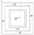
図1に示されるように、半導体装置1は、外周領域に設けられる入出力回路(IO)領域2と、内側領域に配置され、所定の機能を有するASIC(application specific integrated circuit)として構成されるコアロジック領域3と、IO領域2の外側に設けられたパッド5とを備える。
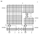
図2に示されるように、各領域にそれぞれ独立に接地電位線が設けられている。
本例においては、デジタル系同士の接地電位線DVSS1と、接地電位線DVSS2との間には、1段の双方向ダイオード素子10が設けられる。
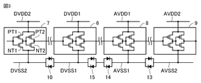
図3に示されるように、デジタルIO回路領域7には、一例として、入力信号を受けて動作するインバータが2段設けられている。
本例においては、それぞれが独立した接地電位線に関して、放電経路を設ける必要があるため双方向ダイオード素子を設けている。たとえば、接地電位線DVSS1と、接地電位線DVSS2との間には、双方向ダイオード素子10が設けられている。
図4は、実施形態の変形例1に従う各回路領域の構成の概念を示す図である。
具体的には、インバータの入力ゲートに対して、ESD破壊防止用のNチャネルMOSトランジスタ50をクランプ回路として設けた点が異なる。
図5は、実施形態の変形例2に従う各回路領域の構成の概念を示す図である。
Claims (7)
- 第1および第2デジタル回路と、
前記第1および第2デジタル回路にそれぞれ対応して設けられた第1および第2接地電位線と、
第1および第2アナログ回路と、
前記第1および第2アナログ回路にそれぞれ対応して設けられた第3および第4接地電位線と、
前記第1接地電位線と前記第2接地電位線との間に設けられた第1双方向ダイオード群と、
前記第3接地電位線と前記第4接地電位線との間に設けられた第2双方向ダイオード群と、
前記第1接地電位線と前記第3接地電位線との間に設けられた第3双方向ダイオード群とを備え、
前記第3双方向ダイオード群は、前記第1および第2双方向ダイオード群がそれぞれ有する双方向ダイオード段数よりも多い、半導体装置。 - 前記第1および第2双方向ダイオード群は、1段で構成され、前記第3双方向ダイオード群は、2段以上で構成される、請求項1記載の半導体装置。
- 前記第1双方向ダイオード群は、前記第1デジタル回路が設けられるデジタルコア領域と、前記第2デジタル回路が設けられるデジタル入出力領域との間に設けられ、
前記第2双方向ダイオード群は、前記第1アナログ回路が設けられるアナログコア領域と、前記第2アナログ回路が設けられるアナログ入出力領域との間に設けられ、
前記第3双方向ダイオード群は、前記デジタルコア領域と、前記アナログコア領域との間に設けられる、請求項1記載の半導体装置。 - 前記第2接地電位線と前記第4接地電位線との間に設けられ、前記第1および第2双方向ダイオード群がそれぞれ有する双方向ダイオード段数よりも多い第4双方向ダイオード群をさらに備え、
前記第4双方向ダイオード群は、前記デジタル入出力領域と前記アナログ入出力領域との間に設けられる、請求項3記載の半導体装置。 - 前記第1アナログ回路は、入力ゲートを含む第1トランジスタ素子と、前記入力ゲートと前記第3接地電位線との間に設けられる第1クランプ素子とをさらに含む、請求項1記載の半導体装置。
- 前記第2アナログ回路は、入力ゲートを含む第2トランジスタ素子と、前記入力ゲートと前記第4接地電位線との間に設けられる第2クランプ素子とをさらに含み、
前記第1クランプ素子のサイズは、前記第2クランプ素子よりも大きい、請求項5記載の半導体装置。 - 前記第1クランプ素子は、前記入力ゲートと前記第3接地電位線との間に接続され、ゲートが前記第3接地電位線と接続されたNチャネルMOSトランジスタで構成される、請求項5記載の半導体装置。
Priority Applications (6)
| Application Number | Priority Date | Filing Date | Title |
|---|---|---|---|
| JP2016094296A JP6595948B2 (ja) | 2016-05-10 | 2016-05-10 | 半導体装置 |
| US15/469,450 US10424920B2 (en) | 2016-05-10 | 2017-03-24 | Semiconductor device |
| TW106113542A TW201806125A (zh) | 2016-05-10 | 2017-04-24 | 半導體裝置 |
| CN201710271669.8A CN107359161B (zh) | 2016-05-10 | 2017-04-24 | 半导体器件 |
| KR1020170056860A KR20170126797A (ko) | 2016-05-10 | 2017-05-04 | 반도체 장치 |
| US16/522,879 US11201465B2 (en) | 2016-05-10 | 2019-07-26 | Semiconductor device |
Applications Claiming Priority (1)
| Application Number | Priority Date | Filing Date | Title |
|---|---|---|---|
| JP2016094296A JP6595948B2 (ja) | 2016-05-10 | 2016-05-10 | 半導体装置 |
Publications (2)
| Publication Number | Publication Date |
|---|---|
| JP2017204516A true JP2017204516A (ja) | 2017-11-16 |
| JP6595948B2 JP6595948B2 (ja) | 2019-10-23 |
Family
ID=60271519
Family Applications (1)
| Application Number | Title | Priority Date | Filing Date |
|---|---|---|---|
| JP2016094296A Active JP6595948B2 (ja) | 2016-05-10 | 2016-05-10 | 半導体装置 |
Country Status (5)
| Country | Link |
|---|---|
| US (2) | US10424920B2 (ja) |
| JP (1) | JP6595948B2 (ja) |
| KR (1) | KR20170126797A (ja) |
| CN (1) | CN107359161B (ja) |
| TW (1) | TW201806125A (ja) |
Cited By (1)
| Publication number | Priority date | Publication date | Assignee | Title |
|---|---|---|---|---|
| JP7596236B2 (ja) | 2020-12-25 | 2024-12-09 | 株式会社東芝 | 半導体装置 |
Families Citing this family (1)
| Publication number | Priority date | Publication date | Assignee | Title |
|---|---|---|---|---|
| CN117254682B (zh) * | 2023-11-20 | 2024-03-12 | 成都芯翼科技有限公司 | 一种抗干扰电压转换电路 |
Citations (4)
| Publication number | Priority date | Publication date | Assignee | Title |
|---|---|---|---|---|
| JPH0855965A (ja) * | 1994-06-13 | 1996-02-27 | Symbios Logic Inc | 過電圧保護機構を有する集積回路およびその保護方法 |
| JP2001185686A (ja) * | 1999-12-24 | 2001-07-06 | Seiko Epson Corp | 半導体集積装置 |
| JP2006319267A (ja) * | 2005-05-16 | 2006-11-24 | Sanyo Electric Co Ltd | 半導体集積回路 |
| JP2011082544A (ja) * | 2003-02-27 | 2011-04-21 | Renesas Electronics Corp | 半導体集積回路装置、半導体集積回路装置の設計方法 |
Family Cites Families (9)
| Publication number | Priority date | Publication date | Assignee | Title |
|---|---|---|---|---|
| US6075686A (en) * | 1997-07-09 | 2000-06-13 | Industrial Technology Research Institute | ESD protection circuit for mixed mode integrated circuits with separated power pins |
| US5991135A (en) * | 1998-05-11 | 1999-11-23 | Vlsi Technology, Inc. | System including ESD protection |
| US7649214B2 (en) * | 2005-10-17 | 2010-01-19 | Taiwan Semiconductor Manufacturing Co., Ltd. | ESD protection system for multiple-domain integrated circuits |
| JP5532566B2 (ja) | 2008-09-24 | 2014-06-25 | セイコーエプソン株式会社 | 半導体装置 |
| JP2011096879A (ja) * | 2009-10-30 | 2011-05-12 | Panasonic Corp | 半導体集積回路 |
| CN102208407A (zh) * | 2010-03-31 | 2011-10-05 | 上海宏力半导体制造有限公司 | 复合电源电路以及双向晶闸管 |
| JP5719126B2 (ja) * | 2010-06-16 | 2015-05-13 | ルネサスエレクトロニクス株式会社 | 内部回路と静電保護回路を具備する半導体集積回路 |
| JP2013030573A (ja) * | 2011-07-28 | 2013-02-07 | Elpida Memory Inc | 半導体装置 |
| EP3054481A1 (en) * | 2015-02-04 | 2016-08-10 | Nxp B.V. | Semiconductor device comprising an ESD protection circuit |
-
2016
- 2016-05-10 JP JP2016094296A patent/JP6595948B2/ja active Active
-
2017
- 2017-03-24 US US15/469,450 patent/US10424920B2/en active Active
- 2017-04-24 TW TW106113542A patent/TW201806125A/zh unknown
- 2017-04-24 CN CN201710271669.8A patent/CN107359161B/zh active Active
- 2017-05-04 KR KR1020170056860A patent/KR20170126797A/ko not_active Withdrawn
-
2019
- 2019-07-26 US US16/522,879 patent/US11201465B2/en active Active
Patent Citations (4)
| Publication number | Priority date | Publication date | Assignee | Title |
|---|---|---|---|---|
| JPH0855965A (ja) * | 1994-06-13 | 1996-02-27 | Symbios Logic Inc | 過電圧保護機構を有する集積回路およびその保護方法 |
| JP2001185686A (ja) * | 1999-12-24 | 2001-07-06 | Seiko Epson Corp | 半導体集積装置 |
| JP2011082544A (ja) * | 2003-02-27 | 2011-04-21 | Renesas Electronics Corp | 半導体集積回路装置、半導体集積回路装置の設計方法 |
| JP2006319267A (ja) * | 2005-05-16 | 2006-11-24 | Sanyo Electric Co Ltd | 半導体集積回路 |
Cited By (1)
| Publication number | Priority date | Publication date | Assignee | Title |
|---|---|---|---|---|
| JP7596236B2 (ja) | 2020-12-25 | 2024-12-09 | 株式会社東芝 | 半導体装置 |
Also Published As
| Publication number | Publication date |
|---|---|
| US20190348835A1 (en) | 2019-11-14 |
| JP6595948B2 (ja) | 2019-10-23 |
| US20170331284A1 (en) | 2017-11-16 |
| KR20170126797A (ko) | 2017-11-20 |
| CN107359161B (zh) | 2023-06-23 |
| US10424920B2 (en) | 2019-09-24 |
| US11201465B2 (en) | 2021-12-14 |
| TW201806125A (zh) | 2018-02-16 |
| CN107359161A (zh) | 2017-11-17 |
Similar Documents
| Publication | Publication Date | Title |
|---|---|---|
| JP3990352B2 (ja) | 半導体集積回路装置 | |
| US8830640B2 (en) | Electrostatic discharge protection circuit | |
| US7755870B2 (en) | Semiconductor integrated circuit device | |
| US20190140641A1 (en) | Semiconductor device including electrostatic protection circuit | |
| CN110767649A (zh) | 集成电路的静电放电防护装置 | |
| US20130114169A1 (en) | Cmos adjustable over voltage esd and surge protection for led application | |
| JP5165356B2 (ja) | 半導体集積回路装置 | |
| TW201203509A (en) | Semiconductor integrated circuit device | |
| US7420789B2 (en) | ESD protection system for multi-power domain circuitry | |
| TW201841334A (zh) | 半導體裝置 | |
| JP2013030573A (ja) | 半導体装置 | |
| JP6595948B2 (ja) | 半導体装置 | |
| US10361557B2 (en) | Semiconductor device | |
| US9154133B2 (en) | ESD robust level shifter | |
| JP2011254100A (ja) | 半導体集積回路装置 | |
| US20070091523A1 (en) | ESD protection system for multi-power domain circuitry | |
| JP2011119415A (ja) | 半導体集積装置 | |
| JP2015095541A (ja) | サージ保護装置 | |
| US6052269A (en) | Electrostatic discharge protection circuit using point discharge | |
| JP5819489B2 (ja) | 半導体装置 | |
| KR100631957B1 (ko) | 정전기 방전 보호 회로 | |
| JP2006093598A (ja) | 半導体集積回路 | |
| JP7455016B2 (ja) | 半導体装置 | |
| KR20080111670A (ko) | 정전기 방전 보호 회로 및 이를 포함하는 반도체 장치 | |
| KR20140119943A (ko) | 정전기 보호 기능을 갖는 반도체 소자 및 정전기 방지 소자 |
Legal Events
| Date | Code | Title | Description |
|---|---|---|---|
| A621 | Written request for application examination |
Free format text: JAPANESE INTERMEDIATE CODE: A621 Effective date: 20181112 |
|
| A977 | Report on retrieval |
Free format text: JAPANESE INTERMEDIATE CODE: A971007 Effective date: 20190827 |
|
| TRDD | Decision of grant or rejection written | ||
| A01 | Written decision to grant a patent or to grant a registration (utility model) |
Free format text: JAPANESE INTERMEDIATE CODE: A01 Effective date: 20190903 |
|
| A61 | First payment of annual fees (during grant procedure) |
Free format text: JAPANESE INTERMEDIATE CODE: A61 Effective date: 20190927 |
|
| R150 | Certificate of patent or registration of utility model |
Ref document number: 6595948 Country of ref document: JP Free format text: JAPANESE INTERMEDIATE CODE: R150 |