JP2017204528A - Solid-state image pickup device - Google Patents
Solid-state image pickup device Download PDFInfo
- Publication number
- JP2017204528A JP2017204528A JP2016094610A JP2016094610A JP2017204528A JP 2017204528 A JP2017204528 A JP 2017204528A JP 2016094610 A JP2016094610 A JP 2016094610A JP 2016094610 A JP2016094610 A JP 2016094610A JP 2017204528 A JP2017204528 A JP 2017204528A
- Authority
- JP
- Japan
- Prior art keywords
- diffusion layer
- photodiode
- distance
- gate electrode
- solid
- Prior art date
- Legal status (The legal status is an assumption and is not a legal conclusion. Google has not performed a legal analysis and makes no representation as to the accuracy of the status listed.)
- Withdrawn
Links
Images
Classifications
-
- H—ELECTRICITY
- H10—SEMICONDUCTOR DEVICES; ELECTRIC SOLID-STATE DEVICES NOT OTHERWISE PROVIDED FOR
- H10F—INORGANIC SEMICONDUCTOR DEVICES SENSITIVE TO INFRARED RADIATION, LIGHT, ELECTROMAGNETIC RADIATION OF SHORTER WAVELENGTH OR CORPUSCULAR RADIATION
- H10F39/00—Integrated devices, or assemblies of multiple devices, comprising at least one element covered by group H10F30/00, e.g. radiation detectors comprising photodiode arrays
- H10F39/80—Constructional details of image sensors
- H10F39/802—Geometry or disposition of elements in pixels, e.g. address-lines or gate electrodes
- H10F39/8023—Disposition of the elements in pixels, e.g. smaller elements in the centre of the imager compared to larger elements at the periphery
-
- H—ELECTRICITY
- H10—SEMICONDUCTOR DEVICES; ELECTRIC SOLID-STATE DEVICES NOT OTHERWISE PROVIDED FOR
- H10F—INORGANIC SEMICONDUCTOR DEVICES SENSITIVE TO INFRARED RADIATION, LIGHT, ELECTROMAGNETIC RADIATION OF SHORTER WAVELENGTH OR CORPUSCULAR RADIATION
- H10F39/00—Integrated devices, or assemblies of multiple devices, comprising at least one element covered by group H10F30/00, e.g. radiation detectors comprising photodiode arrays
- H10F39/80—Constructional details of image sensors
- H10F39/803—Pixels having integrated switching, control, storage or amplification elements
- H10F39/8033—Photosensitive area
-
- H—ELECTRICITY
- H10—SEMICONDUCTOR DEVICES; ELECTRIC SOLID-STATE DEVICES NOT OTHERWISE PROVIDED FOR
- H10F—INORGANIC SEMICONDUCTOR DEVICES SENSITIVE TO INFRARED RADIATION, LIGHT, ELECTROMAGNETIC RADIATION OF SHORTER WAVELENGTH OR CORPUSCULAR RADIATION
- H10F39/00—Integrated devices, or assemblies of multiple devices, comprising at least one element covered by group H10F30/00, e.g. radiation detectors comprising photodiode arrays
- H10F39/10—Integrated devices
- H10F39/12—Image sensors
- H10F39/18—Complementary metal-oxide-semiconductor [CMOS] image sensors; Photodiode array image sensors
-
- H—ELECTRICITY
- H10—SEMICONDUCTOR DEVICES; ELECTRIC SOLID-STATE DEVICES NOT OTHERWISE PROVIDED FOR
- H10F—INORGANIC SEMICONDUCTOR DEVICES SENSITIVE TO INFRARED RADIATION, LIGHT, ELECTROMAGNETIC RADIATION OF SHORTER WAVELENGTH OR CORPUSCULAR RADIATION
- H10F39/00—Integrated devices, or assemblies of multiple devices, comprising at least one element covered by group H10F30/00, e.g. radiation detectors comprising photodiode arrays
- H10F39/80—Constructional details of image sensors
- H10F39/803—Pixels having integrated switching, control, storage or amplification elements
- H10F39/8037—Pixels having integrated switching, control, storage or amplification elements the integrated elements comprising a transistor
Landscapes
- Solid State Image Pick-Up Elements (AREA)
- Transforming Light Signals Into Electric Signals (AREA)
Abstract
【課題】電荷転送の経路の転送トランジスターからフローティングディフュージョンまでのポテンシャル分布の同一性を向上させた固体撮像素子を提供する。【解決手段】本発明は、PD1と第1ゲート電極15と第1FD21を含む第1転送トランジスターTX1と、PD2と第2ゲート電極16と第2FD22を含む第2転送トランジスターTX2と、PD3と第3ゲート電極17と第3FD23を含む第3転送トランジスターTX3と、ソースまたはドレイン領域の拡散層25とリセットゲート27を含むリセットトランジスターRSTと、を有し、前記第1〜第3FD及び前記拡散層25は、互いに離間しており、前記第1〜第3FD及び前記拡散層25は、互いに配線34を介して電気的に接続されており、前記PD1、前記PD2及び前記PD3は一次元状に配列されている固体撮像素子である。【選択図】図1Kind Code: A1 A solid-state imaging device is provided in which uniformity of potential distribution from a transfer transistor in a charge transfer path to a floating diffusion is improved. A first transfer transistor TX1 including a PD1, a first gate electrode 15 and a first FD21; a second transfer transistor TX2 including a PD2, a second gate electrode 16 and a second FD22; A third transfer transistor TX3 including a gate electrode 17 and a third FD 23, and a reset transistor RST including a diffusion layer 25 in a source or drain region and a reset gate 27, wherein the first to third FDs and the diffusion layer 25 are , are separated from each other, the first to third FDs and the diffusion layer 25 are electrically connected to each other through a wiring 34, and the PD1, the PD2, and the PD3 are arranged one-dimensionally. It is a solid-state imaging device with [Selection drawing] Fig. 1
Description
本発明は、固体撮像装置に関する。 The present invention relates to a solid-state imaging device.
CMOSラインセンサーの画素は、フォトダイオード(PD)、転送トランジスター(TX)、増幅トランジスター(Amp)、リセットトランジスター(RST)を基本構成とする。市場からの小型化、多画素化の要請により、画素ピッチは年々微細化されてきたが、画素構成にトランジスターの数が多いCMOSセンサーは、微細化に伴い、PDの開口率が低下し、感度が低下する問題があった。 The pixel of the CMOS line sensor has a basic configuration of a photodiode (PD), a transfer transistor (TX), an amplification transistor (Amp), and a reset transistor (RST). The pixel pitch has been miniaturized year by year due to the demand for miniaturization and multi-pixels from the market. However, the CMOS sensor with a large number of transistors in the pixel configuration has decreased the aperture ratio of the PD and the sensitivity. There was a problem that decreased.
そこで、PDの開口率を上げるために、特許文献1には、隣接する2画素のPDから電荷を転送するTXのフローティングディフュージョン(FD)と、このFDに接続されるRSTを共有させることが記載されている。この場合、TXからFDの中心までの距離は、いずれの画素でも同一になる。 Therefore, in order to increase the aperture ratio of the PD, Patent Document 1 describes that the TX floating diffusion (FD) that transfers charges from the PDs of two adjacent pixels and the RST connected to the FD are shared. Has been. In this case, the distance from TX to the center of the FD is the same for any pixel.
しかしながら、特許文献1に記載の共有方法を延長して、一次元状に並んだ3画素以上のPDに適用しようとすると、TXからFDの中心までの距離を同一にすることができない。そのため、電荷転送の流れ(経路)の上流側にあるTXからFDの中心までのポテンシャル分布が異なり、転送度合に影響を与えてしまう。その結果、特性の画素間ばらつきに影響を与えることがある。つまり、一次元状に並んだ3画素以上のPDの出力部を画素間で共有する場合、TXからFDの中心までの距離が変わってしまうという問題が生じ、このような場合、画素間の特性ばらつきが生じることがある。 However, if the sharing method described in Patent Document 1 is extended and applied to a PD having three or more pixels arranged in a one-dimensional shape, the distance from TX to the center of the FD cannot be made the same. Therefore, the potential distribution from TX to the center of the FD on the upstream side of the charge transfer flow (path) is different, which affects the transfer degree. As a result, it may affect the variation in characteristics between pixels. That is, when the output portion of a PD having three or more pixels arranged in a one-dimensional manner is shared between the pixels, there arises a problem that the distance from the TX to the center of the FD changes. Variations may occur.
本発明の幾つかの態様は、一次元状に配列した3画素以上のフォトダイオードを共有しても、電荷転送の経路の上流側にある転送トランジスターからフローティングディフュージョンまでのポテンシャル分布の同一性を向上させた固体撮像素子に関連している。 Some aspects of the present invention improve the identity of the potential distribution from the transfer transistor on the upstream side of the charge transfer path to the floating diffusion even if the photodiodes of three or more pixels arranged in one dimension are shared Related to the solid-state imaging device.
本発明の第1の態様は、第1フォトダイオードと第1ゲート電極と第1拡散層を含む第1転送トランジスターと、第2フォトダイオードと第2ゲート電極と第2拡散層を含む第2転送トランジスターと、第3フォトダイオードと第3ゲート電極と第3拡散層を含む第3転送トランジスターと、第4拡散層と第4ゲート電極を含むリセットトランジスターと、を有し、前記第1拡散層、前記第2拡散層、前記第3拡散層及び前記第4拡散層は、互いに離間しており、前記第1拡散層、前記第2拡散層、前記第3拡散層及び前記第4拡散層は、互いに配線を介して電気的に接続されており、前記第1フォトダイオード、前記第2フォトダイオード及び前記第3フォトダイオードは一次元状に配列されている固体撮像素子である。 According to a first aspect of the present invention, a first transfer transistor including a first photodiode, a first gate electrode, and a first diffusion layer, a second transfer including a second photodiode, a second gate electrode, and a second diffusion layer are provided. A first transfer layer comprising: a transistor; a third transfer transistor including a third photodiode, a third gate electrode, and a third diffusion layer; and a reset transistor including a fourth diffusion layer and a fourth gate electrode. The second diffusion layer, the third diffusion layer, and the fourth diffusion layer are separated from each other, and the first diffusion layer, the second diffusion layer, the third diffusion layer, and the fourth diffusion layer are: The first photodiode, the second photodiode, and the third photodiode are solid-state imaging elements that are electrically connected to each other via a wiring, and are arranged in a one-dimensional manner.
本発明の第1の態様によれば、第1〜第4拡散層を互いに離間して配置し、第1〜第4拡散層を互いに配線を介して電気的に接続させる。このため、一次元状に配列されたフォトダイオードを共有しても、電荷転送の経路の上流側にある転送トランジスターから拡散層までのポテンシャル分布の同一性を向上させることができる。 According to the first aspect of the present invention, the first to fourth diffusion layers are arranged apart from each other, and the first to fourth diffusion layers are electrically connected to each other via the wiring. For this reason, even if photodiodes arranged one-dimensionally are shared, it is possible to improve the identity of the potential distribution from the transfer transistor on the upstream side of the charge transfer path to the diffusion layer.
本発明の第2の態様は、本発明の第1の態様において、前記第1拡散層、前記第2拡散層及び前記第3拡散層それぞれは形状と面積が略等しいとよい。これにより、電荷転送の経路の上流側にある転送トランジスターから拡散層までのポテンシャル分布の同一性をより向上させることができる。 According to a second aspect of the present invention, in the first aspect of the present invention, each of the first diffusion layer, the second diffusion layer, and the third diffusion layer may have substantially the same shape and area. Thereby, the identity of the potential distribution from the transfer transistor on the upstream side of the charge transfer path to the diffusion layer can be further improved.
本発明の第3の態様は、本発明の第1または第2の態様において、平面視で、前記第1ゲート電極の前記第1フォトダイオード側の端部から前記第1拡散層の中心までの距離と、前記第2ゲート電極の前記第2フォトダイオード側の端部から前記第2拡散層の中心までの距離と、前記第3ゲート電極の前記第3フォトダイオード側の端部から前記第3拡散層の中心までの距離が略等しいとよい。これにより、電荷転送の経路の上流側にある転送トランジスターから拡散層までのポテンシャル分布の同一性をさらに向上させることができる。 According to a third aspect of the present invention, in the first or second aspect of the present invention, from the end of the first gate electrode on the first photodiode side to the center of the first diffusion layer in a plan view. The distance from the end of the second gate electrode on the second photodiode side to the center of the second diffusion layer, and the end of the third gate electrode on the third photodiode side The distances to the center of the diffusion layer are preferably substantially equal. Thereby, the identity of the potential distribution from the transfer transistor on the upstream side of the charge transfer path to the diffusion layer can be further improved.
本発明の第4の態様は、第1フォトダイオードと第1ゲート電極と第1拡散層を含む第1転送トランジスターと、第2フォトダイオードと第2ゲート電極と前記第1拡散層を含む第2転送トランジスターと、第3フォトダイオードと第3ゲート電極と第2拡散層を含む第3転送トランジスターと、第3拡散層と第4ゲート電極を含むリセットトランジスターと、を有し、前記第1拡散層、前記第2拡散層及び前記第3拡散層は、互いに離間しており、前記第1拡散層、前記第2拡散層及び前記第3拡散層は、互いに配線を介して電気的に接続されており、前記第1フォトダイオード、前記第2フォトダイオード及び前記第3フォトダイオードは一次元状に配列されている固体撮像素子である。 According to a fourth aspect of the present invention, there is provided a first transfer transistor including a first photodiode, a first gate electrode, and a first diffusion layer, a second photodiode, a second gate electrode, and a second transfer layer including the first diffusion layer. A transfer transistor; a third transfer transistor including a third photodiode, a third gate electrode, and a second diffusion layer; and a reset transistor including a third diffusion layer and a fourth gate electrode. The second diffusion layer and the third diffusion layer are separated from each other, and the first diffusion layer, the second diffusion layer, and the third diffusion layer are electrically connected to each other through a wiring. The first photodiode, the second photodiode, and the third photodiode are solid-state imaging elements arranged in a one-dimensional manner.
本発明の第4の態様によれば、第1〜第3拡散層を互いに離間して配置し、第1〜第3拡散層を互いに配線を介して接続させる。このため、一次元状に配列されたフォトダイオードを共有しても、電荷転送の経路の上流側にある転送トランジスターから拡散層までのポテンシャル分布の同一性を向上させることができる。 According to the fourth aspect of the present invention, the first to third diffusion layers are arranged apart from each other, and the first to third diffusion layers are connected to each other via the wiring. For this reason, even if photodiodes arranged one-dimensionally are shared, it is possible to improve the identity of the potential distribution from the transfer transistor on the upstream side of the charge transfer path to the diffusion layer.
本発明の第5の態様は、本発明の第4の態様において、前記第1拡散層及び前記第2拡散層それぞれは形状と面積が略等しいとよい。これにより、電荷転送の経路の上流側にある転送トランジスターから拡散層までのポテンシャル分布の同一性をより向上させることができる。 According to a fifth aspect of the present invention, in the fourth aspect of the present invention, each of the first diffusion layer and the second diffusion layer may have substantially the same shape and area. Thereby, the identity of the potential distribution from the transfer transistor on the upstream side of the charge transfer path to the diffusion layer can be further improved.
本発明の第6の態様は、本発明の第4または第5の態様において、第4フォトダイオードと第4ゲート電極と前記第2拡散層を含む第4転送トランジスターを有し、前記第1フォトダイオード、前記第2フォトダイオード、前記第3フォトダイオード及び前記第4フォトダイオードは一次元状に配列されているとよい。 According to a sixth aspect of the present invention, in the fourth or fifth aspect of the present invention, the sixth aspect includes a fourth transfer transistor including a fourth photodiode, a fourth gate electrode, and the second diffusion layer. The diode, the second photodiode, the third photodiode, and the fourth photodiode may be arranged one-dimensionally.
本発明の第7の態様は、本発明の第4乃至第6の態様のいずれか一の態様において、平面視で、前記第1ゲート電極の前記第1フォトダイオード側の端部から前記第1拡散層の中心までの距離と、前記第2ゲート電極の前記第2フォトダイオード側の端部から前記第1拡散層の中心までの距離と、前記第3ゲート電極の前記第3フォトダイオード側の端部から前記第2拡散層の中心までの距離が略等しいとよい。これにより、電荷転送の経路の上流側にある転送トランジスターから拡散層までのポテンシャル分布の同一性をさらに向上させることができる。 According to a seventh aspect of the present invention, in any one of the fourth to sixth aspects of the present invention, the first gate electrode from the end on the first photodiode side in the plan view. The distance to the center of the diffusion layer, the distance from the end of the second gate electrode on the second photodiode side to the center of the first diffusion layer, and the third gate electrode on the third photodiode side The distance from the end to the center of the second diffusion layer is preferably substantially equal. Thereby, the identity of the potential distribution from the transfer transistor on the upstream side of the charge transfer path to the diffusion layer can be further improved.
本発明の第8の態様は、本発明の第6の態様において、平面視で、前記第1ゲート電極の前記第1フォトダイオード側の端部から前記第1拡散層の中心までの距離と、前記第2ゲート電極の前記第2フォトダイオード側の端部から前記第1拡散層の中心までの距離と、前記第3ゲート電極の前記第3フォトダイオード側の端部から前記第2拡散層の中心までの距離と、前記第4ゲート電極の前記第4フォトダイオード側の端部から前記第2拡散層の中心までの距離が等しいとよい。これにより、電荷転送の経路の上流側にある転送トランジスターから拡散層までのポテンシャル分布の同一性をさらに向上させることができる。 According to an eighth aspect of the present invention, in the sixth aspect of the present invention, the distance from the end of the first gate electrode on the first photodiode side to the center of the first diffusion layer in plan view, The distance from the end of the second gate electrode on the second photodiode side to the center of the first diffusion layer, and the end of the third gate electrode on the third photodiode side of the second diffusion layer The distance to the center is preferably equal to the distance from the end of the fourth gate electrode on the fourth photodiode side to the center of the second diffusion layer. Thereby, the identity of the potential distribution from the transfer transistor on the upstream side of the charge transfer path to the diffusion layer can be further improved.
以下、本発明の実施形態について、図面を参照しながら詳細に説明する。ただし、本発明は以下の説明に限定されず、本発明の趣旨及びその範囲から逸脱することなくその形態及び詳細を様々に変更し得ることは、当業者であれば容易に理解される。従って、本発明は以下に示す実施形態の記載内容に限定して解釈されるものではない。 Hereinafter, embodiments of the present invention will be described in detail with reference to the drawings. However, the present invention is not limited to the following description, and it will be easily understood by those skilled in the art that modes and details can be variously changed without departing from the spirit and scope of the present invention. Therefore, the present invention should not be construed as being limited to the description of the embodiments below.
[実施の形態1]
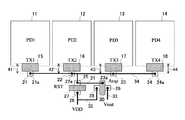
図1は、本発明の一態様に係る固体撮像装置を模式的に示す平面図である。
この固体撮像装置は、一次元状に配列された第1フォトダイオード(PD1)11、第2フォトダイオード(PD2)12、第3フォトダイオード(PD3)13及び第4フォトダイオード(PD4)14を有している。
[Embodiment 1]
FIG. 1 is a plan view schematically showing a solid-state imaging device according to one aspect of the present invention.
This solid-state imaging device has a first photodiode (PD1) 11, a second photodiode (PD2) 12, a third photodiode (PD3) 13, and a fourth photodiode (PD4) 14 arranged in a one-dimensional manner. doing.
また、固体撮像装置は、第1〜第4転送トランジスターTX1,TX2,TX3,TX4、リセットトランジスターRST及び増幅トランジスターAmpを有している。 The solid-state imaging device includes first to fourth transfer transistors TX1, TX2, TX3, TX4, a reset transistor RST, and an amplification transistor Amp.
第1転送トランジスターTX1は、第1フォトダイオード11と第1転送ゲート(第1ゲート電極ともいう。)15と第1フローティングディフュージョン(第1拡散層ともいう。)21によって構成されている。
The first transfer transistor TX1 includes a
第2転送トランジスターTX2は、第2フォトダイオード12と第2転送ゲート(第2ゲート電極ともいう。)16と第2フローティングディフュージョン(第2拡散層ともいう。)22によって構成されている。
The second transfer transistor TX2 includes a
第3転送トランジスターTX3は、第3フォトダイオード13と第3転送ゲート(第3ゲート電極ともいう。)17と第3フローティングディフュージョン(第3拡散層ともいう。)23によって構成されている。
The third transfer transistor TX3 includes a
第4転送トランジスターTX4は、第4フォトダイオード14と第4転送ゲート18と第4フローティングディフュージョン24によって構成されている。
The fourth transfer transistor TX4 includes a
なお、本実施の形態では、4つのフォトダイオードを有する固体撮像装置について説明するが、少なくとも3つのフォトダイオードを有する固体撮像装置であればよく、5つ以上のフォトダイオードを有する固体撮像装置であってもよい。3つのフォトダイオードを有する固体撮像装置の場合は、図1の第4フォトダイオード14及び第4転送トランジスターを削除した構成であればよく、5つ以上のフォトダイオードを有する固体撮像装置の場合は、図1の第4フォトダイオード14及び第4転送トランジスターの隣に5つ目以降のフォトダイオード及び転送トランジスターを同様に一次元状に配列すればよい。
Note that although a solid-state imaging device having four photodiodes is described in this embodiment mode, any solid-state imaging device having at least three photodiodes may be used, and the solid-state imaging device having five or more photodiodes. May be. In the case of a solid-state imaging device having three photodiodes, it is sufficient that the
第1フローティングディフュージョン21、第2フローティングディフュージョン22、第3フローティングディフュージョン23及び第4フローティングディフュージョン24それぞれは形状と面積が略等しい。ここでいう「それぞれは形状と面積が略等しい」とは、第1〜第4フローティングディフュージョン21〜24を所定の形状と面積に設定した場合、その所定の形状と面積に対して±10%以内の範囲に第1〜第4フローティングディフュージョン21〜24が含まれていることを意味する。
Each of the first floating
また、平面視で、第1距離41と第2距離42と第3距離43と第4距離44は略等しい。ここでいう「第1距離41と第2距離42と第3距離43と第4距離44は略等しい」とは、第1〜第4距離41〜44を所定の距離に設定した場合、その所定の距離に対して±10%以内の範囲に第1〜第4距離41〜44が含まれていることを意味する。
Further, the
第1距離41は、第1転送ゲート15の第1フォトダイオード11側の端部から第1フローティングディフュージョン21の中心21aまでの距離である。第2距離42は、第2転送ゲート16の第2フォトダイオード12側の端部から第2フローティングディフュージョン22の中心22aまでの距離である。第3距離43は、第3転送ゲート17の第3フォトダイオード13側の端部から第3フローティングディフュージョン23の中心23aまでの距離である。第4距離44は、第4転送ゲート18の第4フォトダイオード14側の端部から第4フローティングディフュージョン24の中心24aまでの距離である。
The
リセットトランジスターRSTは、ソースまたはドレイン領域の拡散層(第4拡散層ともいう)25とリセットゲート(第4ゲート電極ともいう。)27とドレインまたはソース領域の拡散層26によって構成されている。
The reset transistor RST includes a diffusion layer (also referred to as a fourth diffusion layer) 25 in the source or drain region, a reset gate (also referred to as a fourth gate electrode) 27, and a
第1フローティングディフュージョン(第1FD)21、第2フローティングディフュージョン(第2FD)22、第3フローティングディフュージョン(第3FD)23、第4フローティングディフュージョン(第4FD)24及びソースまたはドレイン領域の拡散層25は、互いに離間している。そして、第1FD21、第2FD22、第3FD23、第4FD24及びソースまたはドレイン領域の拡散層25は、互いに配線34を介して電気的に接続されている。
The first floating diffusion (first FD) 21, the second floating diffusion (second FD) 22, the third floating diffusion (third FD) 23, the fourth floating diffusion (fourth FD) 24, and the
増幅トランジスターAmpは、ソースまたはドレイン領域の拡散層28と増幅ゲート30とドレインまたはソース領域の拡散層29によって構成されている。リセットトランジスターRSTのソースまたはドレイン領域の拡散層25は、配線31を介して増幅ゲート30に電気的に接続されている。Ampのソースまたはドレイン領域の拡散層28は、配線32を介してRSTのドレインまたはソース領域の拡散層26及びVDDに電気的に接続されている。Ampのドレインまたはソース領域の拡散層29は、配線33を介してVoutに電気的に接続されている。
The amplification transistor Amp includes a
本実施の形態によれば、第1〜第4FD21,22,23,24及びソースまたはドレイン領域の拡散層25を互いに離間して配置し、第1〜第4FD21〜24及びソースまたはドレイン領域の拡散層25を互いに配線34を介して接続させる。このため、一次元状に配列した3画素以上のフォトダイオードの出力部を画素間で共有しても、電荷転送の経路の上流側にある転送トランジスターからフローティングディフュージョンまでのポテンシャル分布の同一性を向上させることができる。つまり、転送トランジスターからフローティングディフュージョンにかけてのポテンシャル分布が画素のフォトダイオードによって異なることがなく、特性の画素間ばらつきを抑制することができる。
According to the present embodiment, the first to
また、本実施の形態では、第1FD21、第2FD22、第3FD23及び第4FD24それぞれの形状と面積を略等しくすることで、電荷転送の経路の上流側にある転送トランジスターからフローティングディフュージョンまでのポテンシャル分布の同一性をより向上させることができる。その結果、特性の画素間ばらつきをより抑制することができる。 In the present embodiment, the shape and area of each of the first FD21, the second FD22, the third FD23, and the fourth FD24 are substantially equal, so that the potential distribution from the transfer transistor on the upstream side of the charge transfer path to the floating diffusion is increased. Identity can be further improved. As a result, variation in characteristics between pixels can be further suppressed.
また、本実施の形態では、平面視で、第1距離41と第2距離42と第3距離43と第4距離44を略等しくすることで、電荷転送の経路の上流側にある転送トランジスターからフローティングディフュージョンまでのポテンシャル分布の同一性をさらに向上させることができる。その結果、特性の画素間ばらつきをさらに抑制することができる。
In the present embodiment, the
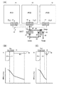
次に、フローティングディフュージョン(FD)70を離間して配置しない比較例について図2を参照しつつ説明する。図2(A)は、比較例としての固体撮像装置を模式的に示す平面図である。図2(B)は、図2(A)に示すA−C間のポテンシャル分布を示す図であり、図2(C)は、図2(A)に示すB−C間のポテンシャル分布を示す図である。 Next, a comparative example in which the floating diffusion (FD) 70 is not arranged separately will be described with reference to FIG. FIG. 2A is a plan view schematically showing a solid-state imaging device as a comparative example. 2B is a diagram showing the potential distribution between A and C shown in FIG. 2A, and FIG. 2C shows the potential distribution between B and C shown in FIG. 2A. FIG.
図2に示す固体撮像装置は、図1に示す固体撮像装置の第4フォトダイオード14及び第4転送トランジスターTX4が無い点と、FD70を離間して配置しない点が図1と相違する。
The solid-state imaging device shown in FIG. 2 is different from FIG. 1 in that the
FD70のポテンシャルの最も低いところは、幾何学的に中心70aとなる地点Cである。リセットトランジスターRSTのソースまたはドレイン領域の拡散層25とFD70を配線によって電気的に接続する際に、FD70へコンタクトを配置する箇所という意味でも、地点Cが最もポテンシャルの低い地点になる。そして、第1転送トランジスターTx1の第1フォトダイオード11側からFD70までの電荷の通過する経路はA−C間となり、第2転送トランジスターTx2の第2フォトダイオード12側からFD70までの電荷の通過する経路はB−C間となる。従って、フローティングディフュージョン(FD)70を図1に示す固体撮像装置のように離間して配置しないと、A−C間とB−C間の経路長(距離)は異なる。
The place where the potential of the
つまり、第1転送ゲート15の第1フォトダイオード11側の端部AからFD70の中心70aの地点CまでのA−C間の経路長は、第2転送ゲート16の第2フォトダイオード12側の端部BからFD70の中心70aの地点CまでのB−C間の経路長より長くなる。そのため、図2(B),(C)に示すように、電位勾配(ポテンシャルスロープ)もA−C間がなだらかとなり、B−C間が急峻となる。その結果、電荷転送の経路の転送トランジスターからFD70までのポテンシャル分布の同一性が低下する。それにより、画素間での特性差が大きくなってしまう。これに対し、図1に示す固体撮像装置では、電荷転送の経路の転送トランジスターからフローティングディフュージョンまでのポテンシャル分布の同一性を向上させているため、画素間での特性差を抑制できる。
That is, the path length between A and C from the end A of the
[実施の形態2]
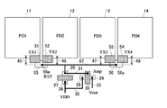
図3は、本発明の一態様に係る固体撮像装置を模式的に示す平面図であり、図1と同一部分には同一符合を付し、同一部分の説明は省略する。
[Embodiment 2]
FIG. 3 is a plan view schematically showing a solid-state imaging device according to an aspect of the present invention. The same parts as those in FIG. 1 are denoted by the same reference numerals, and description of the same parts is omitted.
第1転送トランジスターTX1は、第1フォトダイオード11と第1転送ゲート(第1ゲート電極ともいう。)51と第1フローティングディフュージョン(第1拡散層ともいう。)55によって構成されている。
The first transfer transistor TX <b> 1 includes a
第2転送トランジスターTX2は、第2フォトダイオード12と第2転送ゲート(第2ゲート電極ともいう。)52と第1フローティングディフュージョン55によって構成されている。
The second transfer transistor TX2 includes a
第3転送トランジスターTX3は、第3フォトダイオード13と第3転送ゲート(第3ゲート電極ともいう。)53と第2フローティングディフュージョン(第2拡散層ともいう。)56によって構成されている。
The third transfer transistor TX3 includes a
第4転送トランジスターTX4は、第4フォトダイオード14と第4転送ゲート54と第2フローティングディフュージョン56によって構成されている。
The fourth transfer transistor TX4 includes the
なお、本実施の形態では、4つのフォトダイオードを有する固体撮像装置について説明するが、少なくとも3つのフォトダイオードを有する固体撮像装置であればよく、5つ以上のフォトダイオードを有する固体撮像装置であってもよい。3つのフォトダイオードを有する固体撮像装置の場合は、図3の第4フォトダイオード14及び第4転送ゲート54を削除した構成であればよく、5つ以上のフォトダイオードを有する固体撮像装置の場合は、図3の第4フォトダイオード14及び第4転送トランジスターの隣に5つ目以降のフォトダイオード及び転送トランジスターを同様に一次元状に配列すればよい。
Note that although a solid-state imaging device having four photodiodes is described in this embodiment mode, any solid-state imaging device having at least three photodiodes may be used, and the solid-state imaging device having five or more photodiodes. May be. In the case of a solid-state imaging device having three photodiodes, the configuration may be such that the
第1フローティングディフュージョン(第1FD)55及び第2フローティングディフュージョン(第2FD)56それぞれは形状と面積が略等しい。ここでいう「それぞれは形状と面積が略等しい」とは、第1及び第2FD55,56を所定の形状と面積に設定した場合、その所定の形状と面積に対して±10%以内の範囲に第1及び第2FD55,56が含まれていることを意味する。
Each of the first floating diffusion (first FD) 55 and the second floating diffusion (second FD) 56 has substantially the same shape and area. Here, “each has substantially the same shape and area” means that when the first and
また、平面視で、第1距離45と第2距離46と第3距離47と第4距離48は略等しい。ここでいう「第1距離45と第2距離46と第3距離47と第4距離48は略等しい」とは、第1〜第4距離45〜48を所定の距離に設定した場合、その所定の距離に対して±10%以内の範囲に第1〜第4距離45〜48が含まれていることを意味する。
Further, the
第1距離45は、第1転送ゲート51の第1フォトダイオード11側の端部から第1FD55の中心55aまでの距離である。第2距離46は、第2転送ゲート52の第2フォトダイオード12側の端部から第1FD55の中心55aまでの距離である。第3距離47は、第3転送ゲート53の第3フォトダイオード13側の端部から第2FD56の中心56aまでの距離である。第4距離48は、第4転送ゲート18の第4フォトダイオード14側の端部から第2FD56の中心56aまでの距離である。
The
第1FD55、第2FD56及びソースまたはドレイン領域の拡散層25は、互いに離間している。そして、第1FD55、第2FD56及びソースまたはドレイン領域の拡散層25は、互いに配線57を介して電気的に接続されている。
The first FD 55, the
本実施の形態によれば、第1及び第2FD55,56及びソースまたはドレイン領域の拡散層25を互いに離間して配置し、第1及び第2FD55,56及びソースまたはドレイン領域の拡散層25を互いに配線57を介して接続させる。このため、一次元状に配列した3画素以上のフォトダイオードの出力部を画素間で共有しても、電荷転送の経路の上流側にある転送トランジスターからフローティングディフュージョンまでのポテンシャル分布の同一性を向上させることができる。つまり、転送トランジスターからフローティングディフュージョンにかけてのポテンシャル分布が画素のフォトダイオードによって異なることがなく、特性の画素間ばらつきを抑制することができる。
According to the present embodiment, the first and
また、本実施の形態では、第1FD55及び第2FD56それぞれの形状と面積を略等しくすることで、電荷転送の経路の上流側にある転送トランジスターからフローティングディフュージョンまでのポテンシャル分布の同一性をより向上させることができる。その結果、特性の画素間ばらつきをより抑制することができる。
In the present embodiment, by making the shape and area of each of the first FD 55 and the
また、本実施の形態では、平面視で、第1距離45と第2距離46と第3距離47と第4距離48を略等しくすることで、電荷転送の経路の上流側にある転送トランジスターからフローティングディフュージョンまでのポテンシャル分布の同一性をさらに向上させることができる。その結果、特性の画素間ばらつきをさらに抑制することができる。
In the present embodiment, the
また、上記の実施の形態1〜2を適宜組合せて実施することも可能である。 It is also possible to implement a combination of the above first and second embodiments as appropriate.
11…第1フォトダイオード(PD1)、12…第2フォトダイオード(PD2)、13…第3フォトダイオード(PD3)、14…第4フォトダイオード(PD4)、15…第1転送ゲート、16…第2転送ゲート、17…第3転送ゲート、18…第4転送ゲート、21…第1フローティングディフュージョン、21a…第1フローティングディフュージョンの中心、22…第2フローティングディフュージョン、22a…第2フローティングディフュージョンの中心、23…第3フローティングディフュージョン、23a…第3フローティングディフュージョンの中心、24…第4フローティングディフュージョン、24a…第4フローティングディフュージョンの中心、25…ソースまたはドレイン領域の拡散層、26…ドレインまたはソース領域の拡散層、27…リセットゲート、28…ソースまたはドレイン領域の拡散層、29…ドレインまたはソース領域の拡散層、30…増幅ゲート、31〜34…配線、41…第1距離、42…第2距離、43…第3距離、44…第4距離、45…第1距離、46…第2距離、47…第3距離、48…第4距離、
51…第1転送ゲート、52…第2転送ゲート、53…第3転送ゲート、54…第4転送ゲート、55…第1フローティングディフュージョン、55a…第1フローティングディフュージョンの中心、56…第2フローティングディフュージョン、56a…第2フローティングディフュージョンの中心、57…配線、TX1…第1転送トランジスター、TX2…第2転送トランジスター、TX3…第3転送トランジスター、TX4…第4転送トランジスター、RST…リセットトランジスター、Amp…増幅トランジスター。
DESCRIPTION OF
DESCRIPTION OF
Claims (8)
第2フォトダイオードと第2ゲート電極と第2拡散層を含む第2転送トランジスターと、
第3フォトダイオードと第3ゲート電極と第3拡散層を含む第3転送トランジスターと、
第4拡散層と第4ゲート電極を含むリセットトランジスターと、
を有し、
前記第1拡散層、前記第2拡散層、前記第3拡散層及び前記第4拡散層は、互いに離間しており、
前記第1拡散層、前記第2拡散層、前記第3拡散層及び前記第4拡散層は、互いに配線を介して電気的に接続されており、
前記第1フォトダイオード、前記第2フォトダイオード及び前記第3フォトダイオードは一次元状に配列されている固体撮像素子。 A first transfer transistor including a first photodiode, a first gate electrode, and a first diffusion layer;
A second transfer transistor including a second photodiode, a second gate electrode, and a second diffusion layer;
A third transfer transistor including a third photodiode, a third gate electrode, and a third diffusion layer;
A reset transistor including a fourth diffusion layer and a fourth gate electrode;
Have
The first diffusion layer, the second diffusion layer, the third diffusion layer, and the fourth diffusion layer are spaced apart from each other;
The first diffusion layer, the second diffusion layer, the third diffusion layer, and the fourth diffusion layer are electrically connected to each other via a wiring,
The solid-state imaging device in which the first photodiode, the second photodiode, and the third photodiode are arranged one-dimensionally.
第2フォトダイオードと第2ゲート電極と前記第1拡散層を含む第2転送トランジスターと、
第3フォトダイオードと第3ゲート電極と第2拡散層を含む第3転送トランジスターと、
第3拡散層と第4ゲート電極を含むリセットトランジスターと、
を有し、
前記第1拡散層、前記第2拡散層及び前記第3拡散層は、互いに離間しており、
前記第1拡散層、前記第2拡散層及び前記第3拡散層は、互いに配線を介して電気的に接続されており、
前記第1フォトダイオード、前記第2フォトダイオード及び前記第3フォトダイオードは一次元状に配列されている固体撮像素子。 A first transfer transistor including a first photodiode, a first gate electrode, and a first diffusion layer;
A second transfer transistor including a second photodiode, a second gate electrode, and the first diffusion layer;
A third transfer transistor including a third photodiode, a third gate electrode, and a second diffusion layer;
A reset transistor including a third diffusion layer and a fourth gate electrode;
Have
The first diffusion layer, the second diffusion layer and the third diffusion layer are spaced apart from each other;
The first diffusion layer, the second diffusion layer, and the third diffusion layer are electrically connected to each other via a wiring,
The solid-state imaging device in which the first photodiode, the second photodiode, and the third photodiode are arranged one-dimensionally.
前記第1フォトダイオード、前記第2フォトダイオード、前記第3フォトダイオード及び前記第4フォトダイオードは一次元状に配列されている請求項4または5に記載の固体撮像素子。 A fourth transfer transistor including a fourth photodiode, a fourth gate electrode, and the second diffusion layer;
6. The solid-state imaging device according to claim 4, wherein the first photodiode, the second photodiode, the third photodiode, and the fourth photodiode are arranged one-dimensionally.
Priority Applications (3)
| Application Number | Priority Date | Filing Date | Title |
|---|---|---|---|
| JP2016094610A JP2017204528A (en) | 2016-05-10 | 2016-05-10 | Solid-state image pickup device |
| CN201710220833.2A CN107359171B (en) | 2016-05-10 | 2017-04-06 | solid state imaging device |
| US15/581,812 US10020333B2 (en) | 2016-05-10 | 2017-04-28 | Solid-state imaging device |
Applications Claiming Priority (1)
| Application Number | Priority Date | Filing Date | Title |
|---|---|---|---|
| JP2016094610A JP2017204528A (en) | 2016-05-10 | 2016-05-10 | Solid-state image pickup device |
Publications (2)
| Publication Number | Publication Date |
|---|---|
| JP2017204528A true JP2017204528A (en) | 2017-11-16 |
| JP2017204528A5 JP2017204528A5 (en) | 2019-05-30 |
Family
ID=60271468
Family Applications (1)
| Application Number | Title | Priority Date | Filing Date |
|---|---|---|---|
| JP2016094610A Withdrawn JP2017204528A (en) | 2016-05-10 | 2016-05-10 | Solid-state image pickup device |
Country Status (3)
| Country | Link |
|---|---|
| US (1) | US10020333B2 (en) |
| JP (1) | JP2017204528A (en) |
| CN (1) | CN107359171B (en) |
Cited By (1)
| Publication number | Priority date | Publication date | Assignee | Title |
|---|---|---|---|---|
| US10797100B2 (en) | 2018-09-12 | 2020-10-06 | Kabushiki Kaisha Toshiba | Imaging device |
Citations (4)
| Publication number | Priority date | Publication date | Assignee | Title |
|---|---|---|---|---|
| JP2006073733A (en) * | 2004-09-01 | 2006-03-16 | Canon Inc | Solid-state imaging device and solid-state imaging system |
| JP2007180336A (en) * | 2005-12-28 | 2007-07-12 | Fujitsu Ltd | Semiconductor imaging device |
| JP2012199760A (en) * | 2011-03-22 | 2012-10-18 | Panasonic Corp | Solid-state imaging device |
| JP2013048383A (en) * | 2011-08-29 | 2013-03-07 | Canon Inc | Imaging element and imaging apparatus |
Family Cites Families (10)
| Publication number | Priority date | Publication date | Assignee | Title |
|---|---|---|---|---|
| JP3031606B2 (en) | 1995-08-02 | 2000-04-10 | キヤノン株式会社 | Solid-state imaging device and image imaging device |
| JP3988189B2 (en) | 2002-11-20 | 2007-10-10 | ソニー株式会社 | Solid-state imaging device |
| US7964929B2 (en) * | 2007-08-23 | 2011-06-21 | Aptina Imaging Corporation | Method and apparatus providing imager pixels with shared pixel components |
| JP4760915B2 (en) | 2009-01-08 | 2011-08-31 | ソニー株式会社 | Solid-state image sensor |
| JP5537172B2 (en) * | 2010-01-28 | 2014-07-02 | ソニー株式会社 | Solid-state imaging device and electronic apparatus |
| JP2011159757A (en) * | 2010-01-29 | 2011-08-18 | Sony Corp | Solid-state imaging device and manufacturing method thereof, driving method of solid-state imaging device, and electronic device |
| JP5547150B2 (en) | 2011-09-16 | 2014-07-09 | 株式会社東芝 | Solid-state image sensor |
| JP5911767B2 (en) * | 2012-07-13 | 2016-04-27 | 株式会社東芝 | Solid-state imaging device |
| JP5700106B2 (en) | 2013-12-18 | 2015-04-15 | ソニー株式会社 | Solid-state imaging device and electronic device |
| JP6254048B2 (en) * | 2014-06-05 | 2017-12-27 | ルネサスエレクトロニクス株式会社 | Semiconductor device |
-
2016
- 2016-05-10 JP JP2016094610A patent/JP2017204528A/en not_active Withdrawn
-
2017
- 2017-04-06 CN CN201710220833.2A patent/CN107359171B/en active Active
- 2017-04-28 US US15/581,812 patent/US10020333B2/en active Active
Patent Citations (4)
| Publication number | Priority date | Publication date | Assignee | Title |
|---|---|---|---|---|
| JP2006073733A (en) * | 2004-09-01 | 2006-03-16 | Canon Inc | Solid-state imaging device and solid-state imaging system |
| JP2007180336A (en) * | 2005-12-28 | 2007-07-12 | Fujitsu Ltd | Semiconductor imaging device |
| JP2012199760A (en) * | 2011-03-22 | 2012-10-18 | Panasonic Corp | Solid-state imaging device |
| JP2013048383A (en) * | 2011-08-29 | 2013-03-07 | Canon Inc | Imaging element and imaging apparatus |
Cited By (1)
| Publication number | Priority date | Publication date | Assignee | Title |
|---|---|---|---|---|
| US10797100B2 (en) | 2018-09-12 | 2020-10-06 | Kabushiki Kaisha Toshiba | Imaging device |
Also Published As
| Publication number | Publication date |
|---|---|
| US10020333B2 (en) | 2018-07-10 |
| US20170330904A1 (en) | 2017-11-16 |
| CN107359171B (en) | 2023-04-21 |
| CN107359171A (en) | 2017-11-17 |
Similar Documents
| Publication | Publication Date | Title |
|---|---|---|
| US9026972B2 (en) | Solid-state imaging device, camera, and design method for solid-state imaging device | |
| US9818794B2 (en) | Solid-state image sensor and camera | |
| JP5539104B2 (en) | Photoelectric conversion device and imaging system using the same | |
| TWI566390B (en) | CMOS image sensor that improves pixel dynamic range | |
| US9236406B2 (en) | Photoelectric conversion apparatus with gate control lines and wiring at same height | |
| US10833111B2 (en) | Solid-state imaging apparatus | |
| CN110061026B (en) | Image sensor with shared structure pixel layout | |
| JP2009252782A (en) | Solid-state imaging device | |
| JP2018014409A (en) | Solid state image sensor, method for manufacturing solid state image sensor, and imaging system | |
| US9190439B2 (en) | Solid-state image pickup device | |
| US10276614B2 (en) | Methods and apparatus for an image sensor with a multi-branch transistor | |
| CN104054176A (en) | Image pickup apparatus | |
| US8952476B2 (en) | Solid-state image pickup device | |
| US9654714B2 (en) | Shared pixel with fixed conversion gain | |
| TWI546947B (en) | Shared active pixel sensor | |
| JP2017204528A (en) | Solid-state image pickup device | |
| JP2014146820A (en) | Solid-state image pickup device | |
| KR102944229B1 (en) | Photoelectric conversion device | |
| US9871068B1 (en) | Methods and apparatus for an image sensor with a multi-branch transistor | |
| JP6178835B2 (en) | Solid-state imaging device and camera | |
| JP2017212456A (en) | Solid state image sensor and camera | |
| KR101248805B1 (en) | Solid-state imaging apparatus and method for producing the same | |
| JP2015185699A (en) | Solid-state imaging device and manufacturing method thereof |
Legal Events
| Date | Code | Title | Description |
|---|---|---|---|
| A521 | Request for written amendment filed |
Free format text: JAPANESE INTERMEDIATE CODE: A821 Effective date: 20190411 |
|
| RD04 | Notification of resignation of power of attorney |
Free format text: JAPANESE INTERMEDIATE CODE: A7424 Effective date: 20190411 |
|
| A521 | Request for written amendment filed |
Free format text: JAPANESE INTERMEDIATE CODE: A821 Effective date: 20190412 |
|
| A521 | Request for written amendment filed |
Free format text: JAPANESE INTERMEDIATE CODE: A523 Effective date: 20190416 |
|
| A621 | Written request for application examination |
Free format text: JAPANESE INTERMEDIATE CODE: A621 Effective date: 20190416 |
|
| RD03 | Notification of appointment of power of attorney |
Free format text: JAPANESE INTERMEDIATE CODE: A7423 Effective date: 20190416 |
|
| A977 | Report on retrieval |
Free format text: JAPANESE INTERMEDIATE CODE: A971007 Effective date: 20200310 |
|
| A131 | Notification of reasons for refusal |
Free format text: JAPANESE INTERMEDIATE CODE: A131 Effective date: 20200317 |
|
| A761 | Written withdrawal of application |
Free format text: JAPANESE INTERMEDIATE CODE: A761 Effective date: 20200518 |