JP2017501573A - 光の取り出しが高められた発光ダイオードを備えている光電子デバイス - Google Patents
光の取り出しが高められた発光ダイオードを備えている光電子デバイス Download PDFInfo
- Publication number
- JP2017501573A JP2017501573A JP2016539256A JP2016539256A JP2017501573A JP 2017501573 A JP2017501573 A JP 2017501573A JP 2016539256 A JP2016539256 A JP 2016539256A JP 2016539256 A JP2016539256 A JP 2016539256A JP 2017501573 A JP2017501573 A JP 2017501573A
- Authority
- JP
- Japan
- Prior art keywords
- optoelectronic device
- light emitting
- layer
- wire
- emitting diode
- Prior art date
- Legal status (The legal status is an assumption and is not a legal conclusion. Google has not performed a legal analysis and makes no representation as to the accuracy of the status listed.)
- Granted
Links
Images








Classifications
-
- H—ELECTRICITY
- H10—SEMICONDUCTOR DEVICES; ELECTRIC SOLID-STATE DEVICES NOT OTHERWISE PROVIDED FOR
- H10H—INORGANIC LIGHT-EMITTING SEMICONDUCTOR DEVICES HAVING POTENTIAL BARRIERS
- H10H20/00—Individual inorganic light-emitting semiconductor devices having potential barriers, e.g. light-emitting diodes [LED]
- H10H20/80—Constructional details
- H10H20/81—Bodies
- H10H20/813—Bodies having a plurality of light-emitting regions, e.g. multi-junction LEDs or light-emitting devices having photoluminescent regions within the bodies
-
- H—ELECTRICITY
- H10—SEMICONDUCTOR DEVICES; ELECTRIC SOLID-STATE DEVICES NOT OTHERWISE PROVIDED FOR
- H10H—INORGANIC LIGHT-EMITTING SEMICONDUCTOR DEVICES HAVING POTENTIAL BARRIERS
- H10H20/00—Individual inorganic light-emitting semiconductor devices having potential barriers, e.g. light-emitting diodes [LED]
- H10H20/01—Manufacture or treatment
- H10H20/011—Manufacture or treatment of bodies, e.g. forming semiconductor layers
- H10H20/013—Manufacture or treatment of bodies, e.g. forming semiconductor layers having light-emitting regions comprising only Group III-V materials
- H10H20/0137—Manufacture or treatment of bodies, e.g. forming semiconductor layers having light-emitting regions comprising only Group III-V materials the light-emitting regions comprising nitride materials
-
- H—ELECTRICITY
- H10—SEMICONDUCTOR DEVICES; ELECTRIC SOLID-STATE DEVICES NOT OTHERWISE PROVIDED FOR
- H10H—INORGANIC LIGHT-EMITTING SEMICONDUCTOR DEVICES HAVING POTENTIAL BARRIERS
- H10H20/00—Individual inorganic light-emitting semiconductor devices having potential barriers, e.g. light-emitting diodes [LED]
- H10H20/80—Constructional details
- H10H20/81—Bodies
-
- H—ELECTRICITY
- H10—SEMICONDUCTOR DEVICES; ELECTRIC SOLID-STATE DEVICES NOT OTHERWISE PROVIDED FOR
- H10H—INORGANIC LIGHT-EMITTING SEMICONDUCTOR DEVICES HAVING POTENTIAL BARRIERS
- H10H20/00—Individual inorganic light-emitting semiconductor devices having potential barriers, e.g. light-emitting diodes [LED]
- H10H20/80—Constructional details
- H10H20/81—Bodies
- H10H20/811—Bodies having quantum effect structures or superlattices, e.g. tunnel junctions
- H10H20/812—Bodies having quantum effect structures or superlattices, e.g. tunnel junctions within the light-emitting regions, e.g. having quantum confinement structures
-
- H—ELECTRICITY
- H10—SEMICONDUCTOR DEVICES; ELECTRIC SOLID-STATE DEVICES NOT OTHERWISE PROVIDED FOR
- H10H—INORGANIC LIGHT-EMITTING SEMICONDUCTOR DEVICES HAVING POTENTIAL BARRIERS
- H10H20/00—Individual inorganic light-emitting semiconductor devices having potential barriers, e.g. light-emitting diodes [LED]
- H10H20/80—Constructional details
- H10H20/81—Bodies
- H10H20/816—Bodies having carrier transport control structures, e.g. highly-doped semiconductor layers or current-blocking structures
- H10H20/8162—Current-blocking structures
-
- H—ELECTRICITY
- H10—SEMICONDUCTOR DEVICES; ELECTRIC SOLID-STATE DEVICES NOT OTHERWISE PROVIDED FOR
- H10H—INORGANIC LIGHT-EMITTING SEMICONDUCTOR DEVICES HAVING POTENTIAL BARRIERS
- H10H20/00—Individual inorganic light-emitting semiconductor devices having potential barriers, e.g. light-emitting diodes [LED]
- H10H20/80—Constructional details
- H10H20/81—Bodies
- H10H20/819—Bodies characterised by their shape, e.g. curved or truncated substrates
-
- H—ELECTRICITY
- H10—SEMICONDUCTOR DEVICES; ELECTRIC SOLID-STATE DEVICES NOT OTHERWISE PROVIDED FOR
- H10H—INORGANIC LIGHT-EMITTING SEMICONDUCTOR DEVICES HAVING POTENTIAL BARRIERS
- H10H20/00—Individual inorganic light-emitting semiconductor devices having potential barriers, e.g. light-emitting diodes [LED]
- H10H20/80—Constructional details
- H10H20/81—Bodies
- H10H20/819—Bodies characterised by their shape, e.g. curved or truncated substrates
- H10H20/821—Bodies characterised by their shape, e.g. curved or truncated substrates of the light-emitting regions, e.g. non-planar junctions
-
- H—ELECTRICITY
- H10—SEMICONDUCTOR DEVICES; ELECTRIC SOLID-STATE DEVICES NOT OTHERWISE PROVIDED FOR
- H10H—INORGANIC LIGHT-EMITTING SEMICONDUCTOR DEVICES HAVING POTENTIAL BARRIERS
- H10H20/00—Individual inorganic light-emitting semiconductor devices having potential barriers, e.g. light-emitting diodes [LED]
- H10H20/80—Constructional details
- H10H20/81—Bodies
- H10H20/822—Materials of the light-emitting regions
- H10H20/824—Materials of the light-emitting regions comprising only Group III-V materials, e.g. GaP
- H10H20/825—Materials of the light-emitting regions comprising only Group III-V materials, e.g. GaP containing nitrogen, e.g. GaN
-
- H—ELECTRICITY
- H10—SEMICONDUCTOR DEVICES; ELECTRIC SOLID-STATE DEVICES NOT OTHERWISE PROVIDED FOR
- H10H—INORGANIC LIGHT-EMITTING SEMICONDUCTOR DEVICES HAVING POTENTIAL BARRIERS
- H10H20/00—Individual inorganic light-emitting semiconductor devices having potential barriers, e.g. light-emitting diodes [LED]
- H10H20/80—Constructional details
- H10H20/83—Electrodes
- H10H20/832—Electrodes characterised by their material
- H10H20/833—Transparent materials
-
- H—ELECTRICITY
- H10—SEMICONDUCTOR DEVICES; ELECTRIC SOLID-STATE DEVICES NOT OTHERWISE PROVIDED FOR
- H10H—INORGANIC LIGHT-EMITTING SEMICONDUCTOR DEVICES HAVING POTENTIAL BARRIERS
- H10H20/00—Individual inorganic light-emitting semiconductor devices having potential barriers, e.g. light-emitting diodes [LED]
- H10H20/80—Constructional details
- H10H20/84—Coatings, e.g. passivation layers or antireflective coatings
-
- H—ELECTRICITY
- H10—SEMICONDUCTOR DEVICES; ELECTRIC SOLID-STATE DEVICES NOT OTHERWISE PROVIDED FOR
- H10H—INORGANIC LIGHT-EMITTING SEMICONDUCTOR DEVICES HAVING POTENTIAL BARRIERS
- H10H20/00—Individual inorganic light-emitting semiconductor devices having potential barriers, e.g. light-emitting diodes [LED]
- H10H20/80—Constructional details
- H10H20/84—Coatings, e.g. passivation layers or antireflective coatings
- H10H20/841—Reflective coatings, e.g. dielectric Bragg reflectors
-
- H—ELECTRICITY
- H10—SEMICONDUCTOR DEVICES; ELECTRIC SOLID-STATE DEVICES NOT OTHERWISE PROVIDED FOR
- H10H—INORGANIC LIGHT-EMITTING SEMICONDUCTOR DEVICES HAVING POTENTIAL BARRIERS
- H10H20/00—Individual inorganic light-emitting semiconductor devices having potential barriers, e.g. light-emitting diodes [LED]
- H10H20/80—Constructional details
- H10H20/85—Packages
- H10H20/852—Encapsulations
-
- H—ELECTRICITY
- H10—SEMICONDUCTOR DEVICES; ELECTRIC SOLID-STATE DEVICES NOT OTHERWISE PROVIDED FOR
- H10H—INORGANIC LIGHT-EMITTING SEMICONDUCTOR DEVICES HAVING POTENTIAL BARRIERS
- H10H20/00—Individual inorganic light-emitting semiconductor devices having potential barriers, e.g. light-emitting diodes [LED]
- H10H20/80—Constructional details
- H10H20/85—Packages
- H10H20/852—Encapsulations
- H10H20/853—Encapsulations characterised by their shape
-
- H—ELECTRICITY
- H10—SEMICONDUCTOR DEVICES; ELECTRIC SOLID-STATE DEVICES NOT OTHERWISE PROVIDED FOR
- H10H—INORGANIC LIGHT-EMITTING SEMICONDUCTOR DEVICES HAVING POTENTIAL BARRIERS
- H10H20/00—Individual inorganic light-emitting semiconductor devices having potential barriers, e.g. light-emitting diodes [LED]
- H10H20/80—Constructional details
- H10H20/85—Packages
- H10H20/852—Encapsulations
- H10H20/854—Encapsulations characterised by their material, e.g. epoxy or silicone resins
-
- H—ELECTRICITY
- H10—SEMICONDUCTOR DEVICES; ELECTRIC SOLID-STATE DEVICES NOT OTHERWISE PROVIDED FOR
- H10H—INORGANIC LIGHT-EMITTING SEMICONDUCTOR DEVICES HAVING POTENTIAL BARRIERS
- H10H29/00—Integrated devices, or assemblies of multiple devices, comprising at least one light-emitting semiconductor element covered by group H10H20/00
- H10H29/10—Integrated devices comprising at least one light-emitting semiconductor component covered by group H10H20/00
- H10H29/14—Integrated devices comprising at least one light-emitting semiconductor component covered by group H10H20/00 comprising multiple light-emitting semiconductor components
-
- H—ELECTRICITY
- H10—SEMICONDUCTOR DEVICES; ELECTRIC SOLID-STATE DEVICES NOT OTHERWISE PROVIDED FOR
- H10H—INORGANIC LIGHT-EMITTING SEMICONDUCTOR DEVICES HAVING POTENTIAL BARRIERS
- H10H29/00—Integrated devices, or assemblies of multiple devices, comprising at least one light-emitting semiconductor element covered by group H10H20/00
- H10H29/10—Integrated devices comprising at least one light-emitting semiconductor component covered by group H10H20/00
- H10H29/14—Integrated devices comprising at least one light-emitting semiconductor component covered by group H10H20/00 comprising multiple light-emitting semiconductor components
- H10H29/142—Two-dimensional arrangements, e.g. asymmetric LED layout
-
- H—ELECTRICITY
- H10—SEMICONDUCTOR DEVICES; ELECTRIC SOLID-STATE DEVICES NOT OTHERWISE PROVIDED FOR
- H10W—GENERIC PACKAGES, INTERCONNECTIONS, CONNECTORS OR OTHER CONSTRUCTIONAL DETAILS OF DEVICES COVERED BY CLASS H10
- H10W90/00—Package configurations
-
- H—ELECTRICITY
- H10—SEMICONDUCTOR DEVICES; ELECTRIC SOLID-STATE DEVICES NOT OTHERWISE PROVIDED FOR
- H10H—INORGANIC LIGHT-EMITTING SEMICONDUCTOR DEVICES HAVING POTENTIAL BARRIERS
- H10H20/00—Individual inorganic light-emitting semiconductor devices having potential barriers, e.g. light-emitting diodes [LED]
- H10H20/80—Constructional details
- H10H20/85—Packages
- H10H20/855—Optical field-shaping means, e.g. lenses
Landscapes
- Led Devices (AREA)
- Led Device Packages (AREA)
Abstract
Description
表面を有する半導体基板と、
前記表面に支持され、ワイヤ状、円錐状又は円錐台形状の半導体要素を有する発光ダイオードと、
該発光ダイオードを覆って、1.6 〜1.8 の範囲内の屈折率を有する少なくとも部分的に透明な誘電体層と
を備えていることを特徴とする光電子デバイス
を提供する。
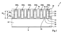
第1の電極8 と、
下面11及び上面12を有する半導体基板10であって、下面11が第1の電極8 で覆われており、上面12が少なくとも発光ダイオードのレベルで好ましくは平面である基板10と、
ワイヤの成長を促す導電性材料から形成され、上面12に配置された複数の成長パッド16と、
成長パッド16の内の1つと夫々接する高さH1のワイヤ20であって、成長パッド16に接する高さH2の下方部分22と、下方部分22に連なる高さH3の上方部分24とを夫々有する複数のワイヤ20(6本のワイヤが示されている)と、
基板10の上面12と、各ワイヤ20の下方部分22の側面とに延びる絶縁層26と、
各上方部分24を覆う半導体層の積層体を有するシェル28と、
各シェル28を覆って絶縁層26上を更に延びる、第2の電極を形成する電極層30と、
ワイヤ20上を延びることなくワイヤ20間の電極層30を覆う導電性のミラー層32と、
構造全体、特に電極層30を覆って、前面36を有する密閉層34と
を備えた構造を示す。
−関連するワイヤ20の上方部分24を覆う活性層、
−活性層を覆う下方部分22の導電型の反対の導電型を有する中間層、及び
−中間層を覆って、電極層30で覆われている接合層
を特に含む複数の層の積層体を有してもよい。
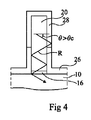
θC =asin(nencap/nwire) (1)
ここで、nencapは密閉層34の光屈折率の実部であり、nwireは、ワイヤ20及びそのシェル28の光屈折率の実部であり、nencapより大きい。
成長パッド16は、上面12に成長層を成膜して成長層の一部を基板10の上面12までエッチングして成長パッドを画定することにより得られてもよい。化学蒸着法(CVD) 又は有機金属気相エピタキシ法(MOVPE) としても知られている有機金属化学蒸着法(MOCVD) のような方法によって成長層を成膜してもよい。しかしながら、分子線エピタキシ法(MBE) 、ガスソースMBE 法(GSMBE) 、有機金属MBE 法(MOMBE) 、プラズマ支援MBE 法(PAMBE) 、原子層エピタキシ法(ALE) 、ハイドライド気相エピタキシ法(HVPE)、及び原子層成膜法(ALD) のような方法を使用してもよい。更に、蒸着法又は反応性カソードスパッタリング法のような方法を使用してもよい。
この工程は、基板10の表面の成長パッド16間に窒化シリコン(例えばSiN 又はSi3N4)の領域を形成する窒化工程によって行われてもよい。この工程は、例えばSiO2、SiN 又はSi3N4の誘電体の層を成膜して成長パッド16間の基板10をマスクし、次に、フォトリソグラフィ工程後に成長パッド16の外側でこの層をエッチングする工程によって行われてもよい。この場合、マスキング層は成長パッド16に亘って延びてもよい。保護する工程(2) が基板10をマスクする工程によって行われる場合、成長層をエッチングする工程は省かれてもよい。そのため、ワイヤが交差する自由な残りの表面を有する均一な連続層から、成長パッド16が形成される。
各ワイヤ20は下にある成長パッド16の最上部から成長する。
上方部分24を成長させるために、MOCVD 反応器内のシランの流れが例えば10分の1以下に減少するか停止することがなければ、MOCVD 反応器の上述した動作条件が一例として維持される。シランの流れが停止する場合であっても、上方部分24は、隣り合う不動態化された部分からのドーパントのこの活性部分における拡散により、又はGaN の残りのドーピングによりN型でドープされてもよい。
下方部分22の周囲を覆う絶縁層26が存在することを考慮すると、シェル28を形成する層の成膜が、絶縁層26で覆われていないワイヤ20の上方部分24のみで生じる。
密閉層34がシリコーンから形成される場合、密閉層34は、スピンコート成膜法、インクジェット法又はシルクスクリーン法によって成膜されてもよい。密閉層34が酸化物である場合、密閉層はCVD によって成膜されてもよい。
Claims (12)
- 表面(12)を有する半導体基板(10)と、
前記表面に支持され、ワイヤ状、円錐状又は円錐台形状の半導体要素(20)を有する発光ダイオード(DEL) と、
該発光ダイオードを覆って、1.6 〜1.8 の範囲内の屈折率及び250 nm〜50μmの範囲内の最大の厚さを有する少なくとも部分的に透明な誘電体層(34)と
を備えていることを特徴とする光電子デバイス(5) 。 - 前記誘電体層(34)の屈折率は、1.7 〜1.75の範囲内であることを特徴とする請求項1に記載の光電子デバイス。
- 前記半導体要素(20)はIII-V 族化合物から主として形成されていることを特徴とする請求項1又は2に記載の光電子デバイス。
- 前記半導体要素(20)は窒化ガリウムを主として含んでいることを特徴とする請求項3に記載の光電子デバイス。
- 前記半導体要素(20)の平均直径は、200 nm〜1μmの範囲内であることを特徴とする請求項1乃至4のいずれかに記載の光電子デバイス。
- 前記誘電体層(34)は、第2の材料の粒子が分散している少なくとも部分的に透明な第1の材料から形成されたマトリクスを有しており、前記第2の材料の屈折率が前記第1の材料の屈折率より大きいことを特徴とする請求項1乃至5のいずれかに記載の光電子デバイス。
- 前記第1の材料はポリシロキサンであることを特徴とする請求項6に記載の光電子デバイス。
- 前記第2の材料は、酸化チタン(TiO2)、酸化ジルコニウム(ZrO2)及び硫化亜鉛(ZnS) から選択された誘電体材料であることを特徴とする請求項6又は7に記載の光電子デバイス。
- 前記誘電体層(34)は、エポキシドポリマー、SiOxタイプの酸化シリコン(ここでxは0より大きく2以下の実数である)、SiOyNzタイプの酸化シリコン(ここでyは0より大きく2以下の実数であり、zは0より大きく0.57以下である)、及び酸化アルミニウム(Al2O3)を含む群から選択された材料から形成されていることを特徴とする請求項1乃至5のいずれかに記載の光電子デバイス。
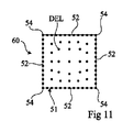
- 前記発光ダイオード(DEL) は、前記表面(12)の一部(51)に亘って分散しており、前記一部における前記発光ダイオード(DEL) の面密度が、前記一部の縁部(52)から離れるにつれて減少することを特徴とする請求項1乃至9のいずれかに記載の光電子デバイス。
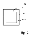
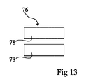
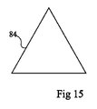
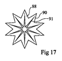
- 前記発光ダイオード(DEL) は、前記表面(12)の一部(70; 76; 80; 84; 86; 88; 94; 96; 98)に亘って分散しており、前記一部の周囲の長さの、前記一部の表面積に対する割合が単位表面積当たり4以上であることを特徴とする請求項1乃至10のいずれかに記載の光電子デバイス。
- 前記一部(70; 90)は、開口した表面に相当することを特徴とする請求項11に記載の光電子デバイス。
Priority Applications (1)
| Application Number | Priority Date | Filing Date | Title |
|---|---|---|---|
| JP2019113054A JP6893954B2 (ja) | 2013-12-19 | 2019-06-18 | 光の取り出しが高められた発光ダイオードを備えている光電子デバイス |
Applications Claiming Priority (3)
| Application Number | Priority Date | Filing Date | Title |
|---|---|---|---|
| FR1363005 | 2013-12-19 | ||
| FR1363005A FR3015772B1 (fr) | 2013-12-19 | 2013-12-19 | Dispositif optoelectronique a diodes electroluminescentes a extraction de lumiere amelioree |
| PCT/EP2014/077418 WO2015091212A1 (fr) | 2013-12-19 | 2014-12-11 | Dispositif optoelectronique a diodes electroluminescentes a extraction de lumiere amelioree |
Related Child Applications (2)
| Application Number | Title | Priority Date | Filing Date |
|---|---|---|---|
| JP2019113055A Division JP2019169735A (ja) | 2013-12-19 | 2019-06-18 | 光の取り出しが高められた発光ダイオードを備えている光電子デバイス |
| JP2019113054A Division JP6893954B2 (ja) | 2013-12-19 | 2019-06-18 | 光の取り出しが高められた発光ダイオードを備えている光電子デバイス |
Publications (2)
| Publication Number | Publication Date |
|---|---|
| JP2017501573A true JP2017501573A (ja) | 2017-01-12 |
| JP6605472B2 JP6605472B2 (ja) | 2019-11-13 |
Family
ID=50102122
Family Applications (3)
| Application Number | Title | Priority Date | Filing Date |
|---|---|---|---|
| JP2016539256A Active JP6605472B2 (ja) | 2013-12-19 | 2014-12-11 | 光の取り出しが高められた発光ダイオードを備えている光電子デバイス |
| JP2019113054A Active JP6893954B2 (ja) | 2013-12-19 | 2019-06-18 | 光の取り出しが高められた発光ダイオードを備えている光電子デバイス |
| JP2019113055A Pending JP2019169735A (ja) | 2013-12-19 | 2019-06-18 | 光の取り出しが高められた発光ダイオードを備えている光電子デバイス |
Family Applications After (2)
| Application Number | Title | Priority Date | Filing Date |
|---|---|---|---|
| JP2019113054A Active JP6893954B2 (ja) | 2013-12-19 | 2019-06-18 | 光の取り出しが高められた発光ダイオードを備えている光電子デバイス |
| JP2019113055A Pending JP2019169735A (ja) | 2013-12-19 | 2019-06-18 | 光の取り出しが高められた発光ダイオードを備えている光電子デバイス |
Country Status (8)
| Country | Link |
|---|---|
| US (3) | US9601543B2 (ja) |
| EP (3) | EP3084846B1 (ja) |
| JP (3) | JP6605472B2 (ja) |
| KR (1) | KR102279462B1 (ja) |
| CN (1) | CN106415858B (ja) |
| FR (1) | FR3015772B1 (ja) |
| TW (3) | TWI656666B (ja) |
| WO (1) | WO2015091212A1 (ja) |
Cited By (1)
| Publication number | Priority date | Publication date | Assignee | Title |
|---|---|---|---|---|
| JP2023508442A (ja) * | 2019-12-26 | 2023-03-02 | アルディア | レーザ切断用の三次元光電子部品を備えたデバイス、及び、このようなデバイスのレーザ切断方法 |
Families Citing this family (13)
| Publication number | Priority date | Publication date | Assignee | Title |
|---|---|---|---|---|
| FR3015772B1 (fr) * | 2013-12-19 | 2017-10-13 | Aledia | Dispositif optoelectronique a diodes electroluminescentes a extraction de lumiere amelioree |
| FR3048817B1 (fr) * | 2016-03-11 | 2018-06-15 | Valeo Comfort And Driving Assistance | Ecran et afficheur tete haute comprenant un tel ecran |
| FR3053530B1 (fr) * | 2016-06-30 | 2018-07-27 | Aledia | Dispositif optoelectronique a pixels a contraste et luminance ameliores |
| FR3053436B1 (fr) * | 2016-07-01 | 2020-07-17 | Valeo Vision | Dispositif d'eclairage et/ou de signalisation pour vehicule automobile |
| CN112262337A (zh) * | 2018-04-25 | 2021-01-22 | 协和(香港)国际教育有限公司 | 用于具有介电层的反射图像显示器的装置和方法 |
| TWI677110B (zh) * | 2018-05-14 | 2019-11-11 | 友達光電股份有限公司 | 微型發光二極體及發光裝置 |
| CN108807610B (zh) * | 2018-06-07 | 2019-12-20 | 台湾创界有限公司 | 微米led线性发光体的制备方法 |
| FR3082657B1 (fr) * | 2018-06-19 | 2021-01-29 | Aledia | Procede de fabrication d’un dispositif optoelectronique a parois de confinement lumineux auto alignes |
| GB2575311B (en) | 2018-07-06 | 2021-03-03 | Plessey Semiconductors Ltd | Monolithic LED array and a precursor thereto |
| FR3087579B1 (fr) * | 2018-10-22 | 2022-08-12 | Aledia | Dispositif optoelectronique a diodes electroluminescentes a extraction de lumiere amelioree |
| FR3091006B1 (fr) * | 2018-12-20 | 2021-01-15 | Commissariat Energie Atomique | Procede de remplissage selectif, par un liquide de remplissage, d’un groupe de cavites parmi une pluralite de cavites |
| WO2021216039A1 (en) * | 2020-04-20 | 2021-10-28 | Google Llc | Nanowire light emitting diodes with directional emission and displays including the same |
| JP7638489B2 (ja) | 2021-02-01 | 2025-03-04 | 豊田合成株式会社 | 半導体素子および半導体素子の製造方法 |
Citations (7)
| Publication number | Priority date | Publication date | Assignee | Title |
|---|---|---|---|---|
| JP2005228936A (ja) * | 2004-02-13 | 2005-08-25 | Dongguk Univ | 発光ダイオードおよびその製造方法 |
| JP2008244302A (ja) * | 2007-03-28 | 2008-10-09 | Matsushita Electric Works Ltd | 化合物半導体発光素子およびそれを用いる照明装置ならびに化合物半導体発光素子の製造方法 |
| JP2009147140A (ja) * | 2007-12-14 | 2009-07-02 | Panasonic Corp | 発光素子および発光素子の製造方法 |
| JP2011501881A (ja) * | 2007-10-22 | 2011-01-13 | コミサリア ア レネルジィ アトミーク エ オ エネルジィ アルタナティブ | ナノワイヤに基づく光電子デバイス及び対応する工程 |
| JP2011134829A (ja) * | 2009-12-24 | 2011-07-07 | Nichia Corp | 発光装置 |
| JP2013055170A (ja) * | 2011-09-02 | 2013-03-21 | Sharp Corp | 自発光ディスプレイおよび自発光ディスプレイの製造方法 |
| US20130313583A1 (en) * | 2012-05-22 | 2013-11-28 | Samsung Electronics Co., Ltd. | Light-emitting device and method of manufacturing the same |
Family Cites Families (20)
| Publication number | Priority date | Publication date | Assignee | Title |
|---|---|---|---|---|
| FR1363005A (fr) | 1963-07-13 | 1964-06-05 | Boehler & Co Ag Geb | Couronne de curetage |
| US20060091411A1 (en) * | 2004-10-29 | 2006-05-04 | Ouderkirk Andrew J | High brightness LED package |
| CN101084112A (zh) * | 2004-11-16 | 2007-12-05 | 奈米晶材照明有限公司 | 以光学上具有可靠的高折射率的纳米粒子为基础的纳米复合封装材料与光子波导材料 |
| JP2006310710A (ja) * | 2005-05-02 | 2006-11-09 | Sony Corp | 半導体発光素子 |
| WO2007001098A1 (en) * | 2005-06-25 | 2007-01-04 | Seoul Opto Device Co., Ltd. | Nanostructure having a nitride-based quantum well and light emitting diode employing the same |
| US8183587B2 (en) * | 2006-12-22 | 2012-05-22 | Qunano Ab | LED with upstanding nanowire structure and method of producing such |
| JP5453105B2 (ja) * | 2006-12-22 | 2014-03-26 | クナノ アーベー | ナノ構造のled及びデバイス |
| KR20110039313A (ko) * | 2008-07-07 | 2011-04-15 | 글로 에이비 | 나노구조 led |
| TWI608760B (zh) * | 2008-11-13 | 2017-12-11 | 行家光電有限公司 | 形成螢光粉轉換發光元件之方法 |
| FR2975532B1 (fr) * | 2011-05-18 | 2013-05-10 | Commissariat Energie Atomique | Connexion electrique en serie de nanofils emetteurs de lumiere |
| KR101769075B1 (ko) * | 2010-12-24 | 2017-08-18 | 서울바이오시스 주식회사 | 발광 다이오드 칩 및 그것을 제조하는 방법 |
| US9204036B2 (en) | 2012-01-31 | 2015-12-01 | Fei Company | Image-enhancing spotlight mode for digital microscopy |
| JP5661671B2 (ja) * | 2012-03-26 | 2015-01-28 | 株式会社東芝 | 半導体発光素子 |
| TWI541992B (zh) * | 2012-05-14 | 2016-07-11 | 國立清華大學 | 發光二極體顯示器與其製造方法 |
| TWI489658B (zh) | 2012-05-25 | 2015-06-21 | 東芝股份有限公司 | 半導體發光裝置及光源單元 |
| KR101891777B1 (ko) * | 2012-06-25 | 2018-08-24 | 삼성전자주식회사 | 유전체 리플렉터를 구비한 발광소자 및 그 제조방법 |
| US9190563B2 (en) * | 2013-11-25 | 2015-11-17 | Samsung Electronics Co., Ltd. | Nanostructure semiconductor light emitting device |
| FR3015772B1 (fr) * | 2013-12-19 | 2017-10-13 | Aledia | Dispositif optoelectronique a diodes electroluminescentes a extraction de lumiere amelioree |
| DE102013114466A1 (de) * | 2013-12-19 | 2015-06-25 | Osram Gmbh | Optoelektronisches Halbleiterbauteil und Verfahren zur Herstellung eines optoelektronischen Halbleiterbauteils |
| KR102227771B1 (ko) * | 2014-08-25 | 2021-03-16 | 삼성전자주식회사 | 나노구조 반도체 발광소자 |
-
2013
- 2013-12-19 FR FR1363005A patent/FR3015772B1/fr not_active Expired - Fee Related
-
2014
- 2014-12-11 KR KR1020167016858A patent/KR102279462B1/ko active Active
- 2014-12-11 EP EP14812451.4A patent/EP3084846B1/fr active Active
- 2014-12-11 CN CN201480069520.6A patent/CN106415858B/zh active Active
- 2014-12-11 EP EP18169638.6A patent/EP3373344B1/fr active Active
- 2014-12-11 US US15/101,887 patent/US9601543B2/en active Active
- 2014-12-11 JP JP2016539256A patent/JP6605472B2/ja active Active
- 2014-12-11 EP EP18169640.2A patent/EP3373345B1/fr active Active
- 2014-12-11 WO PCT/EP2014/077418 patent/WO2015091212A1/fr not_active Ceased
- 2014-12-16 TW TW103143892A patent/TWI656666B/zh active
- 2014-12-16 TW TW108135841A patent/TWI761708B/zh active
- 2014-12-16 TW TW108102133A patent/TWI692886B/zh active
-
2017
- 2017-02-07 US US15/426,690 patent/US10062818B2/en active Active
-
2018
- 2018-03-22 US US15/933,135 patent/US10177288B2/en active Active
-
2019
- 2019-06-18 JP JP2019113054A patent/JP6893954B2/ja active Active
- 2019-06-18 JP JP2019113055A patent/JP2019169735A/ja active Pending
Patent Citations (7)
| Publication number | Priority date | Publication date | Assignee | Title |
|---|---|---|---|---|
| JP2005228936A (ja) * | 2004-02-13 | 2005-08-25 | Dongguk Univ | 発光ダイオードおよびその製造方法 |
| JP2008244302A (ja) * | 2007-03-28 | 2008-10-09 | Matsushita Electric Works Ltd | 化合物半導体発光素子およびそれを用いる照明装置ならびに化合物半導体発光素子の製造方法 |
| JP2011501881A (ja) * | 2007-10-22 | 2011-01-13 | コミサリア ア レネルジィ アトミーク エ オ エネルジィ アルタナティブ | ナノワイヤに基づく光電子デバイス及び対応する工程 |
| JP2009147140A (ja) * | 2007-12-14 | 2009-07-02 | Panasonic Corp | 発光素子および発光素子の製造方法 |
| JP2011134829A (ja) * | 2009-12-24 | 2011-07-07 | Nichia Corp | 発光装置 |
| JP2013055170A (ja) * | 2011-09-02 | 2013-03-21 | Sharp Corp | 自発光ディスプレイおよび自発光ディスプレイの製造方法 |
| US20130313583A1 (en) * | 2012-05-22 | 2013-11-28 | Samsung Electronics Co., Ltd. | Light-emitting device and method of manufacturing the same |
Cited By (2)
| Publication number | Priority date | Publication date | Assignee | Title |
|---|---|---|---|---|
| JP2023508442A (ja) * | 2019-12-26 | 2023-03-02 | アルディア | レーザ切断用の三次元光電子部品を備えたデバイス、及び、このようなデバイスのレーザ切断方法 |
| JP7514560B2 (ja) | 2019-12-26 | 2024-07-11 | アルディア | レーザ切断用の三次元光電子部品を備えたデバイス、及び、このようなデバイスのレーザ切断方法 |
Also Published As
| Publication number | Publication date |
|---|---|
| US20180219143A1 (en) | 2018-08-02 |
| FR3015772B1 (fr) | 2017-10-13 |
| EP3373344B1 (fr) | 2021-03-17 |
| TWI656666B (zh) | 2019-04-11 |
| JP6605472B2 (ja) | 2019-11-13 |
| KR20160100983A (ko) | 2016-08-24 |
| EP3084846B1 (fr) | 2018-07-11 |
| TW201535801A (zh) | 2015-09-16 |
| KR102279462B1 (ko) | 2021-07-19 |
| CN106415858B (zh) | 2019-04-23 |
| EP3373345A1 (fr) | 2018-09-12 |
| TW201921736A (zh) | 2019-06-01 |
| FR3015772A1 (fr) | 2015-06-26 |
| CN106415858A (zh) | 2017-02-15 |
| US10177288B2 (en) | 2019-01-08 |
| US20160307960A1 (en) | 2016-10-20 |
| TW202005123A (zh) | 2020-01-16 |
| US10062818B2 (en) | 2018-08-28 |
| US20170148960A1 (en) | 2017-05-25 |
| EP3373344A1 (fr) | 2018-09-12 |
| US9601543B2 (en) | 2017-03-21 |
| EP3084846A1 (fr) | 2016-10-26 |
| JP6893954B2 (ja) | 2021-06-23 |
| JP2019195077A (ja) | 2019-11-07 |
| TWI692886B (zh) | 2020-05-01 |
| WO2015091212A1 (fr) | 2015-06-25 |
| EP3373345B1 (fr) | 2021-09-15 |
| TWI761708B (zh) | 2022-04-21 |
| JP2019169735A (ja) | 2019-10-03 |
Similar Documents
| Publication | Publication Date | Title |
|---|---|---|
| JP6605472B2 (ja) | 光の取り出しが高められた発光ダイオードを備えている光電子デバイス | |
| TWI745518B (zh) | 具有發光二極體的光電裝置及其製造方法 | |
| JP6382206B2 (ja) | 光電子デバイスを製造する方法 | |
| KR102225302B1 (ko) | 발광 다이오드를 포함하는 광전자 디바이스 | |
| KR102389679B1 (ko) | 3차원 반도체 소자를 구비한 광전자 장치 | |
| TW201839968A (zh) | 具有發光二極體的光電裝置 | |
| CN116601780A (zh) | 具有轴向三维发光二极管的光电设备 | |
| US10026870B2 (en) | Optoelectronic device having semiconductor elements | |
| US20170365737A1 (en) | Optoelectronic device comprising three-dimensional semiconductor elements and method for the production thereof | |
| US9972750B2 (en) | Use of dielectric film to reduce resistivity of transparent conductive oxide in nanowire LEDs | |
| CN112956021B (zh) | 包括发光二极管的具有改进的光提取的光电器件 |
Legal Events
| Date | Code | Title | Description |
|---|---|---|---|
| A621 | Written request for application examination |
Free format text: JAPANESE INTERMEDIATE CODE: A621 Effective date: 20171120 |
|
| A977 | Report on retrieval |
Free format text: JAPANESE INTERMEDIATE CODE: A971007 Effective date: 20180827 |
|
| A131 | Notification of reasons for refusal |
Free format text: JAPANESE INTERMEDIATE CODE: A131 Effective date: 20180918 |
|
| A521 | Request for written amendment filed |
Free format text: JAPANESE INTERMEDIATE CODE: A523 Effective date: 20181210 |
|
| A02 | Decision of refusal |
Free format text: JAPANESE INTERMEDIATE CODE: A02 Effective date: 20190219 |
|
| A521 | Request for written amendment filed |
Free format text: JAPANESE INTERMEDIATE CODE: A523 Effective date: 20190618 |
|
| A521 | Request for written amendment filed |
Free format text: JAPANESE INTERMEDIATE CODE: A821 Effective date: 20190618 |
|
| A911 | Transfer to examiner for re-examination before appeal (zenchi) |
Free format text: JAPANESE INTERMEDIATE CODE: A911 Effective date: 20190708 |
|
| TRDD | Decision of grant or rejection written | ||
| A01 | Written decision to grant a patent or to grant a registration (utility model) |
Free format text: JAPANESE INTERMEDIATE CODE: A01 Effective date: 20191001 |
|
| A61 | First payment of annual fees (during grant procedure) |
Free format text: JAPANESE INTERMEDIATE CODE: A61 Effective date: 20191016 |
|
| R150 | Certificate of patent or registration of utility model |
Ref document number: 6605472 Country of ref document: JP Free format text: JAPANESE INTERMEDIATE CODE: R150 |
|
| R250 | Receipt of annual fees |
Free format text: JAPANESE INTERMEDIATE CODE: R250 |
|
| R250 | Receipt of annual fees |
Free format text: JAPANESE INTERMEDIATE CODE: R250 |
|
| R250 | Receipt of annual fees |
Free format text: JAPANESE INTERMEDIATE CODE: R250 |
|
| R250 | Receipt of annual fees |
Free format text: JAPANESE INTERMEDIATE CODE: R250 |