JP2017506433A - 集積回路抵抗器のための熱金属グラウンド - Google Patents
集積回路抵抗器のための熱金属グラウンド Download PDFInfo
- Publication number
- JP2017506433A JP2017506433A JP2016551306A JP2016551306A JP2017506433A JP 2017506433 A JP2017506433 A JP 2017506433A JP 2016551306 A JP2016551306 A JP 2016551306A JP 2016551306 A JP2016551306 A JP 2016551306A JP 2017506433 A JP2017506433 A JP 2017506433A
- Authority
- JP
- Japan
- Prior art keywords
- integrated circuit
- resistor
- thermal
- metal
- metal region
- Prior art date
- Legal status (The legal status is an assumption and is not a legal conclusion. Google has not performed a legal analysis and makes no representation as to the accuracy of the status listed.)
- Granted
Links
Images


Classifications
-
- H—ELECTRICITY
- H10—SEMICONDUCTOR DEVICES; ELECTRIC SOLID-STATE DEVICES NOT OTHERWISE PROVIDED FOR
- H10D—INORGANIC ELECTRIC SEMICONDUCTOR DEVICES
- H10D1/00—Resistors, capacitors or inductors
- H10D1/40—Resistors
- H10D1/47—Resistors having no potential barriers
- H10D1/474—Resistors having no potential barriers comprising refractory metals, transition metals, noble metals, metal compounds or metal alloys, e.g. silicides
-
- H—ELECTRICITY
- H05—ELECTRIC TECHNIQUES NOT OTHERWISE PROVIDED FOR
- H05K—PRINTED CIRCUITS; CASINGS OR CONSTRUCTIONAL DETAILS OF ELECTRIC APPARATUS; MANUFACTURE OF ASSEMBLAGES OF ELECTRICAL COMPONENTS
- H05K1/00—Printed circuits
- H05K1/02—Details
- H05K1/0201—Thermal arrangements, e.g. for cooling, heating or preventing overheating
- H05K1/0203—Cooling of mounted components
- H05K1/0204—Cooling of mounted components using means for thermal conduction connection in the thickness direction of the substrate
-
- H—ELECTRICITY
- H01—ELECTRIC ELEMENTS
- H01C—RESISTORS
- H01C1/00—Details
- H01C1/01—Mounting; Supporting
-
- H—ELECTRICITY
- H01—ELECTRIC ELEMENTS
- H01C—RESISTORS
- H01C1/00—Details
- H01C1/08—Cooling, heating or ventilating arrangements
-
- H—ELECTRICITY
- H01—ELECTRIC ELEMENTS
- H01C—RESISTORS
- H01C1/00—Details
- H01C1/08—Cooling, heating or ventilating arrangements
- H01C1/084—Cooling, heating or ventilating arrangements using self-cooling, e.g. fins, heat sinks
-
- H—ELECTRICITY
- H10—SEMICONDUCTOR DEVICES; ELECTRIC SOLID-STATE DEVICES NOT OTHERWISE PROVIDED FOR
- H10D—INORGANIC ELECTRIC SEMICONDUCTOR DEVICES
- H10D1/00—Resistors, capacitors or inductors
- H10D1/40—Resistors
- H10D1/47—Resistors having no potential barriers
-
- H—ELECTRICITY
- H10—SEMICONDUCTOR DEVICES; ELECTRIC SOLID-STATE DEVICES NOT OTHERWISE PROVIDED FOR
- H10W—GENERIC PACKAGES, INTERCONNECTIONS, CONNECTORS OR OTHER CONSTRUCTIONAL DETAILS OF DEVICES COVERED BY CLASS H10
- H10W20/00—Interconnections in chips, wafers or substrates
- H10W20/40—Interconnections external to wafers or substrates, e.g. back-end-of-line [BEOL] metallisations or vias connecting to gate electrodes
- H10W20/498—Resistive arrangements or effects of, or between, wiring layers
-
- H—ELECTRICITY
- H10—SEMICONDUCTOR DEVICES; ELECTRIC SOLID-STATE DEVICES NOT OTHERWISE PROVIDED FOR
- H10W—GENERIC PACKAGES, INTERCONNECTIONS, CONNECTORS OR OTHER CONSTRUCTIONAL DETAILS OF DEVICES COVERED BY CLASS H10
- H10W40/00—Arrangements for thermal protection or thermal control
- H10W40/20—Arrangements for cooling
- H10W40/22—Arrangements for cooling characterised by their shape, e.g. having conical or cylindrical projections
- H10W40/226—Arrangements for cooling characterised by their shape, e.g. having conical or cylindrical projections characterised by projecting parts, e.g. fins to increase surface area
- H10W40/228—Arrangements for cooling characterised by their shape, e.g. having conical or cylindrical projections characterised by projecting parts, e.g. fins to increase surface area the projecting parts being wire-shaped or pin-shaped
Landscapes
- Engineering & Computer Science (AREA)
- Microelectronics & Electronic Packaging (AREA)
- Semiconductor Integrated Circuits (AREA)
- Internal Circuitry In Semiconductor Integrated Circuit Devices (AREA)
Abstract
Description
以下に本願の出願当初の特許請求の範囲に記載された発明を付記する。
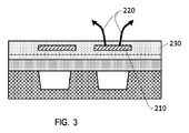
[C1] 集積回路であって、
抵抗器と、
前記抵抗器の少なくとも一部に、オーバーラップし、かつ並行に配置された金属領域と、
前記金属領域に電気的に接続され、かつ前記金属領域と前記抵抗器との間に配置された1つ以上の熱ポストと、前記熱ポストは、前記抵抗器とは電気的に絶縁される、
を備える、集積回路。
[C2] 前記金属領域は、前記集積回路の基板に電気的に接続される、C1に記載の集積回路。
[C3] 前記抵抗器は、窒化チタンで形成される、C1に記載の集積回路。
[C4] 前記金属領域は、前記集積回路の第1の金属層に形成される、C1に記載の集積回路。
[C5] 前記金属領域は、前記抵抗器の上方に配置される、C1に記載の集積回路。
[C6] 前記抵抗器は、誘電体で囲まれる、C1に記載の集積回路。
[C7] 集積回路中の抵抗器から熱を散逸させるための方法であって、
熱金属グラウンドと前記抵抗器との間に配置された1つ以上の熱ポストを使用して、前記抵抗器から前記熱金属グラウンドへ熱を伝導することと、
前記熱金属グラウンドから前記集積回路の基板へ熱を伝導することと、
を備える、方法。
[C8] 前記熱金属グラウンドは、前記抵抗器の少なくとも一部にオーバーラップし、かつ並行に配置される、C7に記載の方法。
[C9] 前記熱ポストは、前記熱金属グラウンドに電気的に接続され、前記熱ポストは、前記抵抗器とは電気的に絶縁される、C7に記載の方法。
[C10] 前記熱金属グラウンドは、前記集積回路の前記基板に電気的に接続される、C7に記載の方法。
[C11] 前記抵抗器は、窒化チタンで形成される、C7に記載の方法。
[C12] 前記熱金属グラウンドは、前記集積回路の第1の金属層に形成される、C7に記載の方法。
[C13] 前記抵抗器は、誘電体で囲まれる、C7に記載の方法。
[C14] 集積回路であって、
抵抗器と、
前記抵抗器の少なくとも一部に、オーバーラップし、かつ並行に配置された金属領域と、
前記抵抗器から前記金属領域へ熱を伝導するための手段と、
を備える集積回路。
[C15] 前記熱を伝導するための手段は、前記金属領域に電気的に接続され、前記金属領域と前記抵抗器との間に配置された1つ以上の熱ポストを含み、前記熱ポストは、前記抵抗器とは電気的に絶縁される、C14に記載の集積回路。
[C16] 前記金属領域は、前記集積回路の基板に電気的に接続される、C14に記載の集積回路。
[C17] 前記抵抗器は、窒化チタンで形成される、C14に記載の集積回路。
[C18] 前記金属領域は、前記集積回路の第1の金属層に形成される、C14に記載の集積回路。
[C19] 前記金属領域は、前記抵抗器の上方に配置される、C14に記載の集積回路。
[C20] 前記抵抗器は、誘電体で囲まれる、C14に記載の集積回路。
Claims (20)
- 集積回路であって、
抵抗器と、
前記抵抗器の少なくとも一部に、オーバーラップし、かつ並行に配置された金属領域と、
前記金属領域に電気的に接続され、かつ前記金属領域と前記抵抗器との間に配置された1つ以上の熱ポストと、前記熱ポストは、前記抵抗器とは電気的に絶縁される、
を備える、集積回路。 - 前記金属領域は、前記集積回路の基板に電気的に接続される、請求項1に記載の集積回路。
- 前記抵抗器は、窒化チタンで形成される、請求項1に記載の集積回路。
- 前記金属領域は、前記集積回路の第1の金属層に形成される、請求項1に記載の集積回路。
- 前記金属領域は、前記抵抗器の上方に配置される、請求項1に記載の集積回路。
- 前記抵抗器は、誘電体で囲まれる、請求項1に記載の集積回路。
- 集積回路中の抵抗器から熱を散逸させるための方法であって、
熱金属グラウンドと前記抵抗器との間に配置された1つ以上の熱ポストを使用して、前記抵抗器から前記熱金属グラウンドへ熱を伝導することと、
前記熱金属グラウンドから前記集積回路の基板へ熱を伝導することと、
を備える、方法。 - 前記熱金属グラウンドは、前記抵抗器の少なくとも一部にオーバーラップし、かつ並行に配置される、請求項7に記載の方法。
- 前記熱ポストは、前記熱金属グラウンドに電気的に接続され、前記熱ポストは、前記抵抗器とは電気的に絶縁される、請求項7に記載の方法。
- 前記熱金属グラウンドは、前記集積回路の前記基板に電気的に接続される、請求項7に記載の方法。
- 前記抵抗器は、窒化チタンで形成される、請求項7に記載の方法。
- 前記熱金属グラウンドは、前記集積回路の第1の金属層に形成される、請求項7に記載の方法。
- 前記抵抗器は、誘電体で囲まれる、請求項7に記載の方法。
- 集積回路であって、
抵抗器と、
前記抵抗器の少なくとも一部に、オーバーラップし、かつ並行に配置された金属領域と、
前記抵抗器から前記金属領域へ熱を伝導するための手段と、
を備える集積回路。 - 前記熱を伝導するための手段は、前記金属領域に電気的に接続され、前記金属領域と前記抵抗器との間に配置された1つ以上の熱ポストを含み、前記熱ポストは、前記抵抗器とは電気的に絶縁される、請求項14に記載の集積回路。
- 前記金属領域は、前記集積回路の基板に電気的に接続される、請求項14に記載の集積回路。
- 前記抵抗器は、窒化チタンで形成される、請求項14に記載の集積回路。
- 前記金属領域は、前記集積回路の第1の金属層に形成される、請求項14に記載の集積回路。
- 前記金属領域は、前記抵抗器の上方に配置される、請求項14に記載の集積回路。
- 前記抵抗器は、誘電体で囲まれる、請求項14に記載の集積回路。
Applications Claiming Priority (3)
| Application Number | Priority Date | Filing Date | Title |
|---|---|---|---|
| US14/181,187 US9930769B2 (en) | 2014-02-14 | 2014-02-14 | Thermal metal ground for integrated circuit resistors |
| US14/181,187 | 2014-02-14 | ||
| PCT/US2015/015041 WO2015123146A1 (en) | 2014-02-14 | 2015-02-09 | Thermal metal ground for integrated circuit resistors |
Publications (3)
| Publication Number | Publication Date |
|---|---|
| JP2017506433A true JP2017506433A (ja) | 2017-03-02 |
| JP2017506433A5 JP2017506433A5 (ja) | 2018-04-05 |
| JP6416272B2 JP6416272B2 (ja) | 2018-10-31 |
Family
ID=52577981
Family Applications (1)
| Application Number | Title | Priority Date | Filing Date |
|---|---|---|---|
| JP2016551306A Active JP6416272B2 (ja) | 2014-02-14 | 2015-02-09 | 集積回路抵抗器のための熱金属グラウンド |
Country Status (7)
| Country | Link |
|---|---|
| US (1) | US9930769B2 (ja) |
| EP (1) | EP3105785B1 (ja) |
| JP (1) | JP6416272B2 (ja) |
| KR (1) | KR101977674B1 (ja) |
| CN (1) | CN105993071B (ja) |
| BR (1) | BR112016018572B1 (ja) |
| WO (1) | WO2015123146A1 (ja) |
Families Citing this family (8)
| Publication number | Priority date | Publication date | Assignee | Title |
|---|---|---|---|---|
| CN106416433B (zh) * | 2014-05-22 | 2019-03-08 | 松下知识产权经营株式会社 | 电路基板 |
| US10304772B2 (en) * | 2017-05-19 | 2019-05-28 | Taiwan Semiconductor Manufacturing Co., Ltd. | Semiconductor device structure with resistive element |
| US10290676B2 (en) * | 2017-08-15 | 2019-05-14 | Northrop Grumman Systems Corporation | Superconducting device with thermally conductive heat sink |
| US10510637B2 (en) | 2017-08-30 | 2019-12-17 | Taiwan Semiconductor Manufacturing Co., Ltd. | Devices and methods for heat dissipation of semiconductor integrated circuits |
| US10475725B2 (en) | 2017-11-08 | 2019-11-12 | Texas Instruments Incorporated | Structure to enable higher current density in integrated circuit resistor |
| US11004763B2 (en) | 2018-12-20 | 2021-05-11 | Northrop Grumman Systems Corporation | Superconducting device with multiple thermal sinks |
| US11522118B2 (en) | 2020-01-09 | 2022-12-06 | Northrop Grumman Systems Corporation | Superconductor structure with normal metal connection to a resistor and method of making the same |
| US11222849B2 (en) | 2020-04-24 | 2022-01-11 | Taiwan Semiconductor Manufacturing Company, Ltd. | Substrate loss reduction for semiconductor devices |
Citations (7)
| Publication number | Priority date | Publication date | Assignee | Title |
|---|---|---|---|---|
| JPH01214048A (ja) * | 1988-02-23 | 1989-08-28 | Fujitsu Ltd | 半導体集積装置 |
| JPH04249360A (ja) * | 1991-02-05 | 1992-09-04 | Nec Ic Microcomput Syst Ltd | 半導体入力保護回路 |
| JPH09252084A (ja) * | 1996-03-15 | 1997-09-22 | Hitachi Ltd | 半導体抵抗装置 |
| JP2000306998A (ja) * | 1999-04-20 | 2000-11-02 | Nec Corp | 半導体装置及びその製造方法 |
| JP2010177506A (ja) * | 2009-01-30 | 2010-08-12 | Nec Corp | 配線基板及びその製造方法 |
| WO2011001494A1 (ja) * | 2009-06-29 | 2011-01-06 | 富士通株式会社 | 半導体装置およびその製造方法 |
| JP2011249430A (ja) * | 2010-05-24 | 2011-12-08 | Panasonic Corp | 半導体装置及び半導体装置の製造方法 |
Family Cites Families (15)
| Publication number | Priority date | Publication date | Assignee | Title |
|---|---|---|---|---|
| JPH04249340A (ja) * | 1991-02-05 | 1992-09-04 | Canon Inc | 半導体ウェハの位置合わせ方法 |
| US6838372B2 (en) * | 2002-09-25 | 2005-01-04 | Cookson Electronics, Inc. | Via interconnect forming process and electronic component product thereof |
| US7345364B2 (en) | 2004-02-04 | 2008-03-18 | Agere Systems Inc. | Structure and method for improved heat conduction for semiconductor devices |
| US7310036B2 (en) * | 2005-01-10 | 2007-12-18 | International Business Machines Corporation | Heat sink for integrated circuit devices |
| US7166913B2 (en) | 2005-04-19 | 2007-01-23 | International Business Machines Corporation | Heat dissipation for heat generating element of semiconductor device and related method |
| JP5005241B2 (ja) * | 2006-03-23 | 2012-08-22 | ルネサスエレクトロニクス株式会社 | 半導体装置及びその製造方法 |
| US8013394B2 (en) | 2007-03-28 | 2011-09-06 | International Business Machines Corporation | Integrated circuit having resistor between BEOL interconnect and FEOL structure and related method |
| US9111779B2 (en) | 2008-08-07 | 2015-08-18 | Texas Instruments Incorporated | IC resistor formed with integral heatsinking structure |
| US8048794B2 (en) * | 2009-08-18 | 2011-11-01 | International Business Machines Corporation | 3D silicon-silicon die stack structure and method for fine pitch interconnection and vertical heat transport |
| US8053870B2 (en) | 2009-12-15 | 2011-11-08 | International Business Machines Corporation | Semiconductor structure incorporating multiple nitride layers to improve thermal dissipation away from a device and a method of forming the structure |
| US8222745B2 (en) * | 2010-01-19 | 2012-07-17 | Lsi Corporation | Integrated heat sink |
| US8848374B2 (en) | 2010-06-30 | 2014-09-30 | Taiwan Semiconductor Manufacturing Company, Ltd. | Method and structure for dissipating heat away from a resistor having neighboring devices and interconnects |
| US8486796B2 (en) | 2010-11-19 | 2013-07-16 | International Business Machines Corporation | Thin film resistors and methods of manufacture |
| US8652922B2 (en) * | 2011-01-18 | 2014-02-18 | International Business Machines Corporation | Compact thermally controlled thin film resistors utilizing substrate contacts and methods of manufacture |
| US8530320B2 (en) * | 2011-06-08 | 2013-09-10 | International Business Machines Corporation | High-nitrogen content metal resistor and method of forming same |
-
2014
- 2014-02-14 US US14/181,187 patent/US9930769B2/en active Active
-
2015
- 2015-02-09 KR KR1020167024109A patent/KR101977674B1/ko not_active Expired - Fee Related
- 2015-02-09 EP EP15706331.4A patent/EP3105785B1/en active Active
- 2015-02-09 BR BR112016018572-2A patent/BR112016018572B1/pt active IP Right Grant
- 2015-02-09 JP JP2016551306A patent/JP6416272B2/ja active Active
- 2015-02-09 CN CN201580008191.9A patent/CN105993071B/zh active Active
- 2015-02-09 WO PCT/US2015/015041 patent/WO2015123146A1/en not_active Ceased
Patent Citations (7)
| Publication number | Priority date | Publication date | Assignee | Title |
|---|---|---|---|---|
| JPH01214048A (ja) * | 1988-02-23 | 1989-08-28 | Fujitsu Ltd | 半導体集積装置 |
| JPH04249360A (ja) * | 1991-02-05 | 1992-09-04 | Nec Ic Microcomput Syst Ltd | 半導体入力保護回路 |
| JPH09252084A (ja) * | 1996-03-15 | 1997-09-22 | Hitachi Ltd | 半導体抵抗装置 |
| JP2000306998A (ja) * | 1999-04-20 | 2000-11-02 | Nec Corp | 半導体装置及びその製造方法 |
| JP2010177506A (ja) * | 2009-01-30 | 2010-08-12 | Nec Corp | 配線基板及びその製造方法 |
| WO2011001494A1 (ja) * | 2009-06-29 | 2011-01-06 | 富士通株式会社 | 半導体装置およびその製造方法 |
| JP2011249430A (ja) * | 2010-05-24 | 2011-12-08 | Panasonic Corp | 半導体装置及び半導体装置の製造方法 |
Also Published As
| Publication number | Publication date |
|---|---|
| EP3105785A1 (en) | 2016-12-21 |
| CN105993071A (zh) | 2016-10-05 |
| US9930769B2 (en) | 2018-03-27 |
| US20150237709A1 (en) | 2015-08-20 |
| EP3105785B1 (en) | 2017-11-22 |
| CN105993071B (zh) | 2019-11-29 |
| BR112016018572A2 (ja) | 2017-08-08 |
| JP6416272B2 (ja) | 2018-10-31 |
| WO2015123146A1 (en) | 2015-08-20 |
| KR20160122177A (ko) | 2016-10-21 |
| KR101977674B1 (ko) | 2019-05-13 |
| BR112016018572B1 (pt) | 2022-04-26 |
Similar Documents
| Publication | Publication Date | Title |
|---|---|---|
| JP6416272B2 (ja) | 集積回路抵抗器のための熱金属グラウンド | |
| US10643986B2 (en) | Power gating for three dimensional integrated circuits (3DIC) | |
| US8881379B2 (en) | Method of making heat sink for integrated circuit devices | |
| TWI527169B (zh) | 半導體裝置及其製造方法以及鰭式場效電晶體 | |
| CN101677102B (zh) | 具有局部互连的半导体器件 | |
| US8222745B2 (en) | Integrated heat sink | |
| CN107785420A (zh) | 半导体器件及其制造方法 | |
| US20130026647A1 (en) | Via structure | |
| CN101728359B (zh) | 半导体器件 | |
| KR102837926B1 (ko) | 집적 회로 칩들의 상호연결 구조물들 | |
| TWI566401B (zh) | 具有低電阻閘極結構之多鰭鰭式場效電晶體 | |
| CN115458504A (zh) | 半导体封装结构及其形成方法 | |
| US7031163B2 (en) | Mechanical cooling fin for interconnects | |
| US20240213252A1 (en) | Vtfet circuit with optimized mol | |
| CN115483182B (zh) | 一种封装结构 | |
| US20240014205A1 (en) | Input/output port circuit and chip thereof | |
| TW202545313A (zh) | 半導體裝置及其製造方法 | |
| CN106548975A (zh) | 半导体结构及其形成方法 | |
| TW201642432A (zh) | 靜電放電防護結構 |
Legal Events
| Date | Code | Title | Description |
|---|---|---|---|
| A521 | Request for written amendment filed |
Free format text: JAPANESE INTERMEDIATE CODE: A523 Effective date: 20161026 Free format text: JAPANESE INTERMEDIATE CODE: A523 Effective date: 20161027 |
|
| A521 | Request for written amendment filed |
Free format text: JAPANESE INTERMEDIATE CODE: A523 Effective date: 20180112 |
|
| A621 | Written request for application examination |
Free format text: JAPANESE INTERMEDIATE CODE: A621 Effective date: 20180112 |
|
| A521 | Request for written amendment filed |
Free format text: JAPANESE INTERMEDIATE CODE: A523 Effective date: 20180220 |
|
| A871 | Explanation of circumstances concerning accelerated examination |
Free format text: JAPANESE INTERMEDIATE CODE: A871 Effective date: 20180220 |
|
| A975 | Report on accelerated examination |
Free format text: JAPANESE INTERMEDIATE CODE: A971005 Effective date: 20180620 |
|
| A131 | Notification of reasons for refusal |
Free format text: JAPANESE INTERMEDIATE CODE: A131 Effective date: 20180626 |
|
| A977 | Report on retrieval |
Free format text: JAPANESE INTERMEDIATE CODE: A971007 Effective date: 20180629 |
|
| A521 | Request for written amendment filed |
Free format text: JAPANESE INTERMEDIATE CODE: A523 Effective date: 20180808 |
|
| TRDD | Decision of grant or rejection written | ||
| A01 | Written decision to grant a patent or to grant a registration (utility model) |
Free format text: JAPANESE INTERMEDIATE CODE: A01 Effective date: 20180904 |
|
| A61 | First payment of annual fees (during grant procedure) |
Free format text: JAPANESE INTERMEDIATE CODE: A61 Effective date: 20181003 |
|
| R150 | Certificate of patent or registration of utility model |
Ref document number: 6416272 Country of ref document: JP Free format text: JAPANESE INTERMEDIATE CODE: R150 |
|
| R250 | Receipt of annual fees |
Free format text: JAPANESE INTERMEDIATE CODE: R250 |
|
| R250 | Receipt of annual fees |
Free format text: JAPANESE INTERMEDIATE CODE: R250 |
|
| R250 | Receipt of annual fees |
Free format text: JAPANESE INTERMEDIATE CODE: R250 |
|
| R250 | Receipt of annual fees |
Free format text: JAPANESE INTERMEDIATE CODE: R250 |
|
| R250 | Receipt of annual fees |
Free format text: JAPANESE INTERMEDIATE CODE: R250 |