JP2017506434A - オプトエレクトロニクス半導体チップの製造方法及びオプトエレクトロニクス半導体チップ - Google Patents
オプトエレクトロニクス半導体チップの製造方法及びオプトエレクトロニクス半導体チップ Download PDFInfo
- Publication number
- JP2017506434A JP2017506434A JP2016552609A JP2016552609A JP2017506434A JP 2017506434 A JP2017506434 A JP 2017506434A JP 2016552609 A JP2016552609 A JP 2016552609A JP 2016552609 A JP2016552609 A JP 2016552609A JP 2017506434 A JP2017506434 A JP 2017506434A
- Authority
- JP
- Japan
- Prior art keywords
- growth
- nucleation layer
- semiconductor
- flat surface
- semiconductor chip
- Prior art date
- Legal status (The legal status is an assumption and is not a legal conclusion. Google has not performed a legal analysis and makes no representation as to the accuracy of the status listed.)
- Granted
Links
Images






Classifications
-
- H—ELECTRICITY
- H10—SEMICONDUCTOR DEVICES; ELECTRIC SOLID-STATE DEVICES NOT OTHERWISE PROVIDED FOR
- H10F—INORGANIC SEMICONDUCTOR DEVICES SENSITIVE TO INFRARED RADIATION, LIGHT, ELECTROMAGNETIC RADIATION OF SHORTER WAVELENGTH OR CORPUSCULAR RADIATION
- H10F71/00—Manufacture or treatment of devices covered by this subclass
- H10F71/127—The active layers comprising only Group III-V materials, e.g. GaAs or InP
- H10F71/1276—The active layers comprising only Group III-V materials, e.g. GaAs or InP comprising growth substrates not made of Group III-V materials
-
- H—ELECTRICITY
- H10—SEMICONDUCTOR DEVICES; ELECTRIC SOLID-STATE DEVICES NOT OTHERWISE PROVIDED FOR
- H10H—INORGANIC LIGHT-EMITTING SEMICONDUCTOR DEVICES HAVING POTENTIAL BARRIERS
- H10H20/00—Individual inorganic light-emitting semiconductor devices having potential barriers, e.g. light-emitting diodes [LED]
- H10H20/01—Manufacture or treatment
-
- H—ELECTRICITY
- H10—SEMICONDUCTOR DEVICES; ELECTRIC SOLID-STATE DEVICES NOT OTHERWISE PROVIDED FOR
- H10F—INORGANIC SEMICONDUCTOR DEVICES SENSITIVE TO INFRARED RADIATION, LIGHT, ELECTROMAGNETIC RADIATION OF SHORTER WAVELENGTH OR CORPUSCULAR RADIATION
- H10F71/00—Manufacture or treatment of devices covered by this subclass
- H10F71/127—The active layers comprising only Group III-V materials, e.g. GaAs or InP
- H10F71/1278—The active layers comprising only Group III-V materials, e.g. GaAs or InP comprising nitrides, e.g. GaN
-
- H—ELECTRICITY
- H10—SEMICONDUCTOR DEVICES; ELECTRIC SOLID-STATE DEVICES NOT OTHERWISE PROVIDED FOR
- H10F—INORGANIC SEMICONDUCTOR DEVICES SENSITIVE TO INFRARED RADIATION, LIGHT, ELECTROMAGNETIC RADIATION OF SHORTER WAVELENGTH OR CORPUSCULAR RADIATION
- H10F77/00—Constructional details of devices covered by this subclass
- H10F77/10—Semiconductor bodies
- H10F77/12—Active materials
- H10F77/124—Active materials comprising only Group III-V materials, e.g. GaAs
- H10F77/1246—III-V nitrides, e.g. GaN
-
- H—ELECTRICITY
- H10—SEMICONDUCTOR DEVICES; ELECTRIC SOLID-STATE DEVICES NOT OTHERWISE PROVIDED FOR
- H10H—INORGANIC LIGHT-EMITTING SEMICONDUCTOR DEVICES HAVING POTENTIAL BARRIERS
- H10H20/00—Individual inorganic light-emitting semiconductor devices having potential barriers, e.g. light-emitting diodes [LED]
- H10H20/01—Manufacture or treatment
- H10H20/011—Manufacture or treatment of bodies, e.g. forming semiconductor layers
- H10H20/013—Manufacture or treatment of bodies, e.g. forming semiconductor layers having light-emitting regions comprising only Group III-V materials
- H10H20/0133—Manufacture or treatment of bodies, e.g. forming semiconductor layers having light-emitting regions comprising only Group III-V materials with a substrate not being Group III-V materials
-
- H—ELECTRICITY
- H10—SEMICONDUCTOR DEVICES; ELECTRIC SOLID-STATE DEVICES NOT OTHERWISE PROVIDED FOR
- H10H—INORGANIC LIGHT-EMITTING SEMICONDUCTOR DEVICES HAVING POTENTIAL BARRIERS
- H10H20/00—Individual inorganic light-emitting semiconductor devices having potential barriers, e.g. light-emitting diodes [LED]
- H10H20/01—Manufacture or treatment
- H10H20/011—Manufacture or treatment of bodies, e.g. forming semiconductor layers
- H10H20/013—Manufacture or treatment of bodies, e.g. forming semiconductor layers having light-emitting regions comprising only Group III-V materials
- H10H20/0133—Manufacture or treatment of bodies, e.g. forming semiconductor layers having light-emitting regions comprising only Group III-V materials with a substrate not being Group III-V materials
- H10H20/01335—Manufacture or treatment of bodies, e.g. forming semiconductor layers having light-emitting regions comprising only Group III-V materials with a substrate not being Group III-V materials the light-emitting regions comprising nitride materials
-
- H—ELECTRICITY
- H10—SEMICONDUCTOR DEVICES; ELECTRIC SOLID-STATE DEVICES NOT OTHERWISE PROVIDED FOR
- H10H—INORGANIC LIGHT-EMITTING SEMICONDUCTOR DEVICES HAVING POTENTIAL BARRIERS
- H10H20/00—Individual inorganic light-emitting semiconductor devices having potential barriers, e.g. light-emitting diodes [LED]
- H10H20/01—Manufacture or treatment
- H10H20/011—Manufacture or treatment of bodies, e.g. forming semiconductor layers
- H10H20/013—Manufacture or treatment of bodies, e.g. forming semiconductor layers having light-emitting regions comprising only Group III-V materials
- H10H20/0137—Manufacture or treatment of bodies, e.g. forming semiconductor layers having light-emitting regions comprising only Group III-V materials the light-emitting regions comprising nitride materials
-
- H—ELECTRICITY
- H10—SEMICONDUCTOR DEVICES; ELECTRIC SOLID-STATE DEVICES NOT OTHERWISE PROVIDED FOR
- H10H—INORGANIC LIGHT-EMITTING SEMICONDUCTOR DEVICES HAVING POTENTIAL BARRIERS
- H10H20/00—Individual inorganic light-emitting semiconductor devices having potential barriers, e.g. light-emitting diodes [LED]
- H10H20/01—Manufacture or treatment
- H10H20/036—Manufacture or treatment of packages
-
- H—ELECTRICITY
- H10—SEMICONDUCTOR DEVICES; ELECTRIC SOLID-STATE DEVICES NOT OTHERWISE PROVIDED FOR
- H10H—INORGANIC LIGHT-EMITTING SEMICONDUCTOR DEVICES HAVING POTENTIAL BARRIERS
- H10H20/00—Individual inorganic light-emitting semiconductor devices having potential barriers, e.g. light-emitting diodes [LED]
- H10H20/80—Constructional details
- H10H20/81—Bodies
-
- H—ELECTRICITY
- H10—SEMICONDUCTOR DEVICES; ELECTRIC SOLID-STATE DEVICES NOT OTHERWISE PROVIDED FOR
- H10H—INORGANIC LIGHT-EMITTING SEMICONDUCTOR DEVICES HAVING POTENTIAL BARRIERS
- H10H20/00—Individual inorganic light-emitting semiconductor devices having potential barriers, e.g. light-emitting diodes [LED]
- H10H20/80—Constructional details
- H10H20/81—Bodies
- H10H20/815—Bodies having stress relaxation structures, e.g. buffer layers
-
- H—ELECTRICITY
- H10—SEMICONDUCTOR DEVICES; ELECTRIC SOLID-STATE DEVICES NOT OTHERWISE PROVIDED FOR
- H10H—INORGANIC LIGHT-EMITTING SEMICONDUCTOR DEVICES HAVING POTENTIAL BARRIERS
- H10H20/00—Individual inorganic light-emitting semiconductor devices having potential barriers, e.g. light-emitting diodes [LED]
- H10H20/80—Constructional details
- H10H20/81—Bodies
- H10H20/819—Bodies characterised by their shape, e.g. curved or truncated substrates
- H10H20/82—Roughened surfaces, e.g. at the interface between epitaxial layers
-
- H—ELECTRICITY
- H10—SEMICONDUCTOR DEVICES; ELECTRIC SOLID-STATE DEVICES NOT OTHERWISE PROVIDED FOR
- H10H—INORGANIC LIGHT-EMITTING SEMICONDUCTOR DEVICES HAVING POTENTIAL BARRIERS
- H10H20/00—Individual inorganic light-emitting semiconductor devices having potential barriers, e.g. light-emitting diodes [LED]
- H10H20/80—Constructional details
- H10H20/81—Bodies
- H10H20/822—Materials of the light-emitting regions
- H10H20/824—Materials of the light-emitting regions comprising only Group III-V materials, e.g. GaP
- H10H20/825—Materials of the light-emitting regions comprising only Group III-V materials, e.g. GaP containing nitrogen, e.g. GaN
-
- H—ELECTRICITY
- H10—SEMICONDUCTOR DEVICES; ELECTRIC SOLID-STATE DEVICES NOT OTHERWISE PROVIDED FOR
- H10P—GENERIC PROCESSES OR APPARATUS FOR THE MANUFACTURE OR TREATMENT OF DEVICES COVERED BY CLASS H10
- H10P14/00—Formation of materials, e.g. in the shape of layers or pillars
- H10P14/20—Formation of materials, e.g. in the shape of layers or pillars of semiconductor materials
- H10P14/27—Formation of materials, e.g. in the shape of layers or pillars of semiconductor materials using selective deposition, e.g. simultaneous growth of monocrystalline and non-monocrystalline semiconductor materials
- H10P14/271—Formation of materials, e.g. in the shape of layers or pillars of semiconductor materials using selective deposition, e.g. simultaneous growth of monocrystalline and non-monocrystalline semiconductor materials characterised by the preparation of substrate for selective deposition
-
- H—ELECTRICITY
- H10—SEMICONDUCTOR DEVICES; ELECTRIC SOLID-STATE DEVICES NOT OTHERWISE PROVIDED FOR
- H10P—GENERIC PROCESSES OR APPARATUS FOR THE MANUFACTURE OR TREATMENT OF DEVICES COVERED BY CLASS H10
- H10P14/00—Formation of materials, e.g. in the shape of layers or pillars
- H10P14/20—Formation of materials, e.g. in the shape of layers or pillars of semiconductor materials
- H10P14/27—Formation of materials, e.g. in the shape of layers or pillars of semiconductor materials using selective deposition, e.g. simultaneous growth of monocrystalline and non-monocrystalline semiconductor materials
- H10P14/276—Lateral overgrowth
-
- H—ELECTRICITY
- H10—SEMICONDUCTOR DEVICES; ELECTRIC SOLID-STATE DEVICES NOT OTHERWISE PROVIDED FOR
- H10P—GENERIC PROCESSES OR APPARATUS FOR THE MANUFACTURE OR TREATMENT OF DEVICES COVERED BY CLASS H10
- H10P14/00—Formation of materials, e.g. in the shape of layers or pillars
- H10P14/20—Formation of materials, e.g. in the shape of layers or pillars of semiconductor materials
- H10P14/29—Formation of materials, e.g. in the shape of layers or pillars of semiconductor materials characterised by the substrates
- H10P14/2924—Structures
- H10P14/2925—Surface structures
-
- H—ELECTRICITY
- H10—SEMICONDUCTOR DEVICES; ELECTRIC SOLID-STATE DEVICES NOT OTHERWISE PROVIDED FOR
- H10P—GENERIC PROCESSES OR APPARATUS FOR THE MANUFACTURE OR TREATMENT OF DEVICES COVERED BY CLASS H10
- H10P14/00—Formation of materials, e.g. in the shape of layers or pillars
- H10P14/20—Formation of materials, e.g. in the shape of layers or pillars of semiconductor materials
- H10P14/32—Formation of materials, e.g. in the shape of layers or pillars of semiconductor materials characterised by intermediate layers between substrates and deposited layers
- H10P14/3202—Materials thereof
- H10P14/3214—Materials thereof being Group IIIA-VA semiconductors
- H10P14/3216—Nitrides
-
- H—ELECTRICITY
- H10—SEMICONDUCTOR DEVICES; ELECTRIC SOLID-STATE DEVICES NOT OTHERWISE PROVIDED FOR
- H10P—GENERIC PROCESSES OR APPARATUS FOR THE MANUFACTURE OR TREATMENT OF DEVICES COVERED BY CLASS H10
- H10P14/00—Formation of materials, e.g. in the shape of layers or pillars
- H10P14/20—Formation of materials, e.g. in the shape of layers or pillars of semiconductor materials
- H10P14/34—Deposited materials, e.g. layers
- H10P14/3402—Deposited materials, e.g. layers characterised by the chemical composition
- H10P14/3414—Deposited materials, e.g. layers characterised by the chemical composition being group IIIA-VIA materials
- H10P14/3416—Nitrides
-
- H—ELECTRICITY
- H10—SEMICONDUCTOR DEVICES; ELECTRIC SOLID-STATE DEVICES NOT OTHERWISE PROVIDED FOR
- H10P—GENERIC PROCESSES OR APPARATUS FOR THE MANUFACTURE OR TREATMENT OF DEVICES COVERED BY CLASS H10
- H10P14/00—Formation of materials, e.g. in the shape of layers or pillars
- H10P14/20—Formation of materials, e.g. in the shape of layers or pillars of semiconductor materials
- H10P14/32—Formation of materials, e.g. in the shape of layers or pillars of semiconductor materials characterised by intermediate layers between substrates and deposited layers
- H10P14/3202—Materials thereof
- H10P14/3238—Materials thereof being insulating materials
Landscapes
- Led Devices (AREA)
- Light Receiving Elements (AREA)
- Crystals, And After-Treatments Of Crystals (AREA)
Abstract
Description
Claims (11)
- エレクトロニクス半導体チップ(100)の製造方法であって、
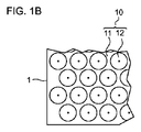
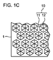
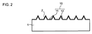
− 平坦な面(11)により形成される成長表面(10)を備えた成長基板(1)を準備するステップであって、前記平坦な面(11)上に三次元的に成形された複数の表面構造(12)を備えている、ステップと
− 前記成長表面(10)上に直接、酸素を含むAlNからなる核形成層(2)を大面積で施すステップと、
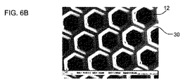
− 前記核形成層(2)上に、窒化物を基礎とする半導体積層部(3)を成長させるステップであって、前記半導体積層部(3)を前記平坦な面(11)から選択的に成長させる、ステップと
を含む、エレクトロニクス半導体チップ(100)の製造方法。 - 前記平坦な面(11)上での前記半導体積層部(3)の選択的な成長を、前記核形成層(2)の酸素含有率によって調節する、請求項1に記載の方法。
- 前記三次元的に成形された表面構造(12)は、前記半導体積層部(3)の成長の際に、前記半導体積層部(3)によりほぼ覆われる、請求項1又は2に記載の方法。
- 有機金属気相成長によって前記核形成層(2)を施す、請求項1から3までのいずれか1項に記載の方法。
- スパッタリングによって前記核形成層(2)を施す、請求項1から3までのいずれか1項に記載の方法。
- 前記三次元的に成形された表面構造(12)を、前記平坦な面(11)上に円錐形の又は角錐形の突出部により形成させる、請求項1から5までのいずれか1項記載の方法。
- 前記成長基板(1)は、酸化アルミニウムを含むか又は酸化アルミニウムからなる、請求項1から6までのいずれか1項に記載の方法。
- 前記平坦な面(11)は、結晶学的c面である、請求項7に記載の方法。
- 前記半導体チップ(100)の作動時に、光の放射又は検出が予定されているオプトエレクトロニクス能動層(34)を備えた前記半導体積層部(3)を成長させる、請求項1から8までのいずれか1項に記載の方法。
- 前記半導体チップ(100)は、発光ダイオード又は光検出ダイオードとして構成される、請求項9に記載の方法。
- − 平坦な面(11)により形成される成長表面(10)を備えた成長基板(1)であって、前記平坦な面(11)上に複数の三次元的に成形された表面構造(12)を備えている、成長基板(1)と、
− 前記成長表面(10)上に直接大面積で施された、酸素を含むAlNからなる核形成層(2)と、
− 前記核形成層(2)上の、窒化物を基礎とする半導体積層部(3)とを備え、
ここで前記半導体積層部(3)は、前記平坦な面(11)から選択的に成長されている、
エレクトロニクス半導体チップ(100)。
Applications Claiming Priority (3)
| Application Number | Priority Date | Filing Date | Title |
|---|---|---|---|
| DE102014101966.0 | 2014-02-17 | ||
| DE102014101966.0A DE102014101966A1 (de) | 2014-02-17 | 2014-02-17 | Verfahren zur Herstellung eines elektronischen Halbleiterchips und elektronischer Halbleiterchip |
| PCT/EP2015/053051 WO2015121399A1 (de) | 2014-02-17 | 2015-02-13 | Verfahren zur herstellung eines optoelektronischen halbleiterchips und optoelektronischer halbleiterchip |
Publications (2)
| Publication Number | Publication Date |
|---|---|
| JP2017506434A true JP2017506434A (ja) | 2017-03-02 |
| JP6472459B2 JP6472459B2 (ja) | 2019-02-20 |
Family
ID=52469842
Family Applications (1)
| Application Number | Title | Priority Date | Filing Date |
|---|---|---|---|
| JP2016552609A Active JP6472459B2 (ja) | 2014-02-17 | 2015-02-13 | オプトエレクトロニクス半導体チップの製造方法及びオプトエレクトロニクス半導体チップ |
Country Status (6)
| Country | Link |
|---|---|
| US (4) | US10312401B2 (ja) |
| JP (1) | JP6472459B2 (ja) |
| KR (3) | KR102380030B1 (ja) |
| CN (1) | CN106030834B (ja) |
| DE (2) | DE102014101966A1 (ja) |
| WO (1) | WO2015121399A1 (ja) |
Cited By (1)
| Publication number | Priority date | Publication date | Assignee | Title |
|---|---|---|---|---|
| WO2019044173A1 (ja) * | 2017-08-31 | 2019-03-07 | 東芝マテリアル株式会社 | 半導体発光素子およびその製造方法 |
Families Citing this family (10)
| Publication number | Priority date | Publication date | Assignee | Title |
|---|---|---|---|---|
| DE102015109761B4 (de) | 2015-06-18 | 2022-01-27 | OSRAM Opto Semiconductors Gesellschaft mit beschränkter Haftung | Verfahren zur Herstellung eines Nitrid-Halbleiterbauelements und Nitrid-Halbleiterbauelement |
| CN105633233B (zh) * | 2015-12-31 | 2018-01-12 | 华灿光电(苏州)有限公司 | AlN模板、AlN模板的制备方法及AlN模板上的半导体器件 |
| CN105470357B (zh) * | 2015-12-31 | 2018-05-22 | 华灿光电(苏州)有限公司 | AlN模板、AlN模板的制备方法及AlN模板上的半导体器件 |
| CN107180884B (zh) * | 2016-03-11 | 2019-04-23 | 中国科学院苏州纳米技术与纳米仿生研究所 | 一种半极性AlN模板 |
| TWI577842B (zh) * | 2016-05-30 | 2017-04-11 | 光鋐科技股份有限公司 | 氮化鋁鎵的成長方法 |
| US20180083163A1 (en) * | 2016-09-21 | 2018-03-22 | Tqyqda Gosei Co. , Ltd. | Light-emitting device and method of manufacturing the same |
| CN109301048A (zh) * | 2018-08-01 | 2019-02-01 | 华灿光电(浙江)有限公司 | 一种氮化镓基发光二极管外延片及其生长方法 |
| CN110504301A (zh) * | 2019-09-09 | 2019-11-26 | 南方科技大学 | 一种iii族氮化物晶体管外延结构和晶体管器件 |
| US20230124414A1 (en) * | 2021-10-14 | 2023-04-20 | Applied Materials, Inc. | SUBSTRATE PROCESSING FOR GaN GROWTH |
| US12557436B2 (en) | 2021-10-14 | 2026-02-17 | Applied Materials, Inc. | Substrate processing for GaN growth |
Citations (3)
| Publication number | Priority date | Publication date | Assignee | Title |
|---|---|---|---|---|
| US20110012109A1 (en) * | 2009-07-17 | 2011-01-20 | Applied Materials, Inc. | Method of forming a group iii-nitride crystalline film on a patterned substrate by hydride vapor phase epitaxy (hvpe) |
| WO2013187171A1 (ja) * | 2012-06-13 | 2013-12-19 | シャープ株式会社 | 窒化物半導体発光素子及びその製造方法 |
| WO2014021259A1 (ja) * | 2012-08-03 | 2014-02-06 | シャープ株式会社 | 窒化物半導体素子構造体とその製造方法 |
Family Cites Families (19)
| Publication number | Priority date | Publication date | Assignee | Title |
|---|---|---|---|---|
| US6744076B2 (en) * | 2002-03-14 | 2004-06-01 | The Circle For The Promotion Of Science And Engineering | Single crystalline aluminum nitride film, method of forming the same, base substrate for group III element nitride film, light emitting device and surface acoustic wave device |
| US6936851B2 (en) * | 2003-03-21 | 2005-08-30 | Tien Yang Wang | Semiconductor light-emitting device and method for manufacturing the same |
| WO2004105108A2 (en) * | 2003-05-21 | 2004-12-02 | Lumilog | Manufacturing gallium nitride substrates by lateral overgrowth through masks and devices fabricated thereof |
| JP5082278B2 (ja) * | 2005-05-16 | 2012-11-28 | ソニー株式会社 | 発光ダイオードの製造方法、集積型発光ダイオードの製造方法および窒化物系iii−v族化合物半導体の成長方法 |
| JP4462249B2 (ja) * | 2005-09-22 | 2010-05-12 | ソニー株式会社 | 発光ダイオードの製造方法、集積型発光ダイオードの製造方法および窒化物系iii−v族化合物半導体の成長方法 |
| TWI288491B (en) * | 2006-03-02 | 2007-10-11 | Nat Univ Chung Hsing | High extraction efficiency of solid-state light emitting device |
| KR101330251B1 (ko) * | 2007-03-06 | 2013-11-15 | 서울바이오시스 주식회사 | 패터닝된 기판 상에 질화물 반도체층을 형성하는 방법 및그것을 갖는 발광 다이오드 |
| JP2009081406A (ja) | 2007-09-27 | 2009-04-16 | Showa Denko Kk | Iii族窒化物半導体発光素子及びその製造方法、並びにランプ |
| US8143647B2 (en) * | 2009-12-18 | 2012-03-27 | Palo Alto Research Center Incorporated | Relaxed InGaN/AlGaN templates |
| EP2362412B1 (en) | 2010-02-19 | 2020-04-08 | Samsung Electronics Co., Ltd. | Method of growing nitride semiconductor |
| KR101180414B1 (ko) * | 2010-09-17 | 2012-09-10 | 주식회사 기가레인 | 고휘도 엘이디 용 기판 구조 및 그 기판에서의 에피택시 기반층 성장방법 |
| WO2012090818A1 (ja) * | 2010-12-29 | 2012-07-05 | シャープ株式会社 | 窒化物半導体構造、窒化物半導体発光素子、窒化物半導体トランジスタ素子、窒化物半導体構造の製造方法および窒化物半導体素子の製造方法 |
| TWI470829B (zh) | 2011-04-27 | 2015-01-21 | Sino American Silicon Prod Inc | 磊晶基板的製作方法、發光二極體,及其製作方法 |
| US8653499B2 (en) | 2011-06-06 | 2014-02-18 | Epistar Corporation | Light-emitting diode with strain-relaxed layer for reducing strain in active layer |
| DE102011114671A1 (de) | 2011-09-30 | 2013-04-04 | Osram Opto Semiconductors Gmbh | Verfahren zur Herstellung eines optoelektronischen Halbleiterchips und optoelektronischer Halbleiterchip |
| KR20130066308A (ko) * | 2011-12-12 | 2013-06-20 | 엘지이노텍 주식회사 | 발광소자 |
| DE102012103686B4 (de) | 2012-04-26 | 2021-07-08 | OSRAM Opto Semiconductors Gesellschaft mit beschränkter Haftung | Epitaxiesubstrat, Verfahren zur Herstellung eines Epitaxiesubstrats und optoelektronischer Halbleiterchip mit einem Epitaxiesubstrat |
| CN102842660B (zh) * | 2012-08-17 | 2015-11-11 | 圆融光电科技有限公司 | 一种氮化镓基发光二极管外延片结构及其制备方法 |
| US9190592B2 (en) * | 2012-11-06 | 2015-11-17 | Nextreme Thermal Solutions, Inc. | Thin film thermoelectric devices having favorable crystal tilt |
-
2014
- 2014-02-17 DE DE102014101966.0A patent/DE102014101966A1/de not_active Withdrawn
-
2015
- 2015-02-13 JP JP2016552609A patent/JP6472459B2/ja active Active
- 2015-02-13 CN CN201580009138.0A patent/CN106030834B/zh active Active
- 2015-02-13 WO PCT/EP2015/053051 patent/WO2015121399A1/de not_active Ceased
- 2015-02-13 KR KR1020217029599A patent/KR102380030B1/ko active Active
- 2015-02-13 US US15/115,242 patent/US10312401B2/en active Active
- 2015-02-13 KR KR1020167021965A patent/KR102232546B1/ko active Active
- 2015-02-13 KR KR1020217008248A patent/KR102304639B1/ko active Active
- 2015-02-13 DE DE112015000824.1T patent/DE112015000824B4/de active Active
-
2019
- 2019-04-15 US US16/384,550 patent/US11005003B2/en active Active
-
2021
- 2021-03-19 US US17/206,911 patent/US11430907B2/en active Active
-
2022
- 2022-07-11 US US17/811,761 patent/US11888083B2/en active Active
Patent Citations (3)
| Publication number | Priority date | Publication date | Assignee | Title |
|---|---|---|---|---|
| US20110012109A1 (en) * | 2009-07-17 | 2011-01-20 | Applied Materials, Inc. | Method of forming a group iii-nitride crystalline film on a patterned substrate by hydride vapor phase epitaxy (hvpe) |
| WO2013187171A1 (ja) * | 2012-06-13 | 2013-12-19 | シャープ株式会社 | 窒化物半導体発光素子及びその製造方法 |
| WO2014021259A1 (ja) * | 2012-08-03 | 2014-02-06 | シャープ株式会社 | 窒化物半導体素子構造体とその製造方法 |
Cited By (5)
| Publication number | Priority date | Publication date | Assignee | Title |
|---|---|---|---|---|
| WO2019044173A1 (ja) * | 2017-08-31 | 2019-03-07 | 東芝マテリアル株式会社 | 半導体発光素子およびその製造方法 |
| KR20200035428A (ko) * | 2017-08-31 | 2020-04-03 | 도시바 마테리알 가부시키가이샤 | 반도체 발광 소자 및 그의 제조 방법 |
| JPWO2019044173A1 (ja) * | 2017-08-31 | 2020-10-29 | 東芝マテリアル株式会社 | 半導体発光素子およびその製造方法 |
| KR102295780B1 (ko) | 2017-08-31 | 2021-09-01 | 도시바 마테리알 가부시키가이샤 | 반도체 발광 소자 및 그의 제조 방법 |
| JP7123322B2 (ja) | 2017-08-31 | 2022-08-23 | 東芝マテリアル株式会社 | 半導体発光素子およびその製造方法 |
Also Published As
| Publication number | Publication date |
|---|---|
| US20220344532A1 (en) | 2022-10-27 |
| US11005003B2 (en) | 2021-05-11 |
| CN106030834A (zh) | 2016-10-12 |
| DE102014101966A1 (de) | 2015-08-20 |
| US20190245110A1 (en) | 2019-08-08 |
| KR20210034113A (ko) | 2021-03-29 |
| US20210210651A1 (en) | 2021-07-08 |
| KR102232546B1 (ko) | 2021-03-26 |
| DE112015000824B4 (de) | 2021-07-08 |
| DE112015000824A5 (de) | 2016-11-03 |
| CN106030834B (zh) | 2020-03-06 |
| KR102304639B1 (ko) | 2021-09-24 |
| KR20210118221A (ko) | 2021-09-29 |
| JP6472459B2 (ja) | 2019-02-20 |
| US11430907B2 (en) | 2022-08-30 |
| US11888083B2 (en) | 2024-01-30 |
| US10312401B2 (en) | 2019-06-04 |
| KR102380030B1 (ko) | 2022-03-29 |
| US20170005223A1 (en) | 2017-01-05 |
| WO2015121399A1 (de) | 2015-08-20 |
| KR20160123300A (ko) | 2016-10-25 |
Similar Documents
| Publication | Publication Date | Title |
|---|---|---|
| JP6472459B2 (ja) | オプトエレクトロニクス半導体チップの製造方法及びオプトエレクトロニクス半導体チップ | |
| TW200814369A (en) | III nitride compound semiconductor laminated structure | |
| JP6686172B2 (ja) | 窒化物半導体発光素子 | |
| US8334156B2 (en) | Nitride semiconductor single crystal substrate, and methods of fabricating the same and a vertical nitride semiconductor light emitting diode using the same | |
| JP2017028076A (ja) | Iii族窒化物発光素子の製造方法 | |
| EP2525417A2 (en) | Nitride semiconductor device, nitride semiconductor wafer and method for manufacturing nitride semiconductor layer | |
| JP5041883B2 (ja) | Iii族窒化物半導体層の製造方法、iii族窒化物半導体発光素子の製造方法 | |
| TWI252599B (en) | N-type group III nitride semiconductor layered structure | |
| JP2012204540A (ja) | 半導体装置およびその製造方法 | |
| JP2021508951A (ja) | 三次元発光ダイオードを備えた光電子デバイス | |
| US11616164B2 (en) | Method for producing a nitride compound semiconductor component | |
| JP2015115343A (ja) | 窒化物半導体素子の製造方法 | |
| JP2008226868A (ja) | Iii族窒化物化合物半導体積層構造体 | |
| JP6242238B2 (ja) | 窒化物半導体多元混晶の製造方法 | |
| JP2015050247A (ja) | 窒化物半導体発光素子の製造方法、窒化物半導体発光素子および窒化物半導体発光素子用下地基板 | |
| JP2009266963A (ja) | 窒化物系発光素子、及び半導体発光素子を製造する方法 | |
| TWI545798B (zh) | Nitride semiconductor light emitting device and manufacturing method thereof | |
| JP4705384B2 (ja) | 窒化ガリウム系半導体素子 | |
| JP2007095786A (ja) | Iii族窒化物系化合物半導体発光素子 | |
| JP2007214378A (ja) | 窒化物系半導体素子 | |
| JP4987240B2 (ja) | 化合物半導体素子、化合物半導体素子の製造方法、ダイオード素子 | |
| TWI596797B (zh) | Gallium nitride-based crystal and semiconductor device manufacturing method, and light-emitting Device and method of manufacturing the light-emitting device | |
| JP2006024903A (ja) | 窒化ガリウム系半導体積層構造体 | |
| JP2006019713A (ja) | Iii族窒化物半導体発光素子およびそれを用いたled | |
| JP2016164905A (ja) | p型GaN層の製造方法、及び該製造方法を利用した半導体デバイスの製造方法 |
Legal Events
| Date | Code | Title | Description |
|---|---|---|---|
| A521 | Request for written amendment filed |
Free format text: JAPANESE INTERMEDIATE CODE: A523 Effective date: 20161017 |
|
| A621 | Written request for application examination |
Free format text: JAPANESE INTERMEDIATE CODE: A621 Effective date: 20161017 |
|
| A977 | Report on retrieval |
Free format text: JAPANESE INTERMEDIATE CODE: A971007 Effective date: 20170927 |
|
| A131 | Notification of reasons for refusal |
Free format text: JAPANESE INTERMEDIATE CODE: A131 Effective date: 20171002 |
|
| A521 | Request for written amendment filed |
Free format text: JAPANESE INTERMEDIATE CODE: A523 Effective date: 20171218 |
|
| A02 | Decision of refusal |
Free format text: JAPANESE INTERMEDIATE CODE: A02 Effective date: 20180604 |
|
| A521 | Request for written amendment filed |
Free format text: JAPANESE INTERMEDIATE CODE: A523 Effective date: 20181004 |
|
| A911 | Transfer to examiner for re-examination before appeal (zenchi) |
Free format text: JAPANESE INTERMEDIATE CODE: A911 Effective date: 20181016 |
|
| A131 | Notification of reasons for refusal |
Free format text: JAPANESE INTERMEDIATE CODE: A131 Effective date: 20181203 |
|
| A521 | Request for written amendment filed |
Free format text: JAPANESE INTERMEDIATE CODE: A523 Effective date: 20181214 |
|
| TRDD | Decision of grant or rejection written | ||
| A01 | Written decision to grant a patent or to grant a registration (utility model) |
Free format text: JAPANESE INTERMEDIATE CODE: A01 Effective date: 20190107 |
|
| A61 | First payment of annual fees (during grant procedure) |
Free format text: JAPANESE INTERMEDIATE CODE: A61 Effective date: 20190122 |
|
| R150 | Certificate of patent or registration of utility model |
Ref document number: 6472459 Country of ref document: JP Free format text: JAPANESE INTERMEDIATE CODE: R150 |
|
| R250 | Receipt of annual fees |
Free format text: JAPANESE INTERMEDIATE CODE: R250 |
|
| R250 | Receipt of annual fees |
Free format text: JAPANESE INTERMEDIATE CODE: R250 |
|
| R250 | Receipt of annual fees |
Free format text: JAPANESE INTERMEDIATE CODE: R250 |
|
| R250 | Receipt of annual fees |
Free format text: JAPANESE INTERMEDIATE CODE: R250 |
|
| R250 | Receipt of annual fees |
Free format text: JAPANESE INTERMEDIATE CODE: R250 |