JP2017509166A - モードファミリーを除去するためのシステム及び方法 - Google Patents
モードファミリーを除去するためのシステム及び方法 Download PDFInfo
- Publication number
- JP2017509166A JP2017509166A JP2016575294A JP2016575294A JP2017509166A JP 2017509166 A JP2017509166 A JP 2017509166A JP 2016575294 A JP2016575294 A JP 2016575294A JP 2016575294 A JP2016575294 A JP 2016575294A JP 2017509166 A JP2017509166 A JP 2017509166A
- Authority
- JP
- Japan
- Prior art keywords
- resonator
- mode
- refractive index
- changing
- families
- Prior art date
- Legal status (The legal status is an assumption and is not a legal conclusion. Google has not performed a legal analysis and makes no representation as to the accuracy of the status listed.)
- Granted
Links
Images



Classifications
-
- H—ELECTRICITY
- H01—ELECTRIC ELEMENTS
- H01S—DEVICES USING THE PROCESS OF LIGHT AMPLIFICATION BY STIMULATED EMISSION OF RADIATION [LASER] TO AMPLIFY OR GENERATE LIGHT; DEVICES USING STIMULATED EMISSION OF ELECTROMAGNETIC RADIATION IN WAVE RANGES OTHER THAN OPTICAL
- H01S3/00—Lasers, i.e. devices using stimulated emission of electromagnetic radiation in the infrared, visible or ultraviolet wave range
- H01S3/05—Construction or shape of optical resonators; Accommodation of active medium therein; Shape of active medium
- H01S3/06—Construction or shape of active medium
- H01S3/0627—Construction or shape of active medium the resonator being monolithic, e.g. microlaser
-
- H—ELECTRICITY
- H01—ELECTRIC ELEMENTS
- H01S—DEVICES USING THE PROCESS OF LIGHT AMPLIFICATION BY STIMULATED EMISSION OF RADIATION [LASER] TO AMPLIFY OR GENERATE LIGHT; DEVICES USING STIMULATED EMISSION OF ELECTROMAGNETIC RADIATION IN WAVE RANGES OTHER THAN OPTICAL
- H01S3/00—Lasers, i.e. devices using stimulated emission of electromagnetic radiation in the infrared, visible or ultraviolet wave range
- H01S3/05—Construction or shape of optical resonators; Accommodation of active medium therein; Shape of active medium
- H01S3/06—Construction or shape of active medium
- H01S3/0602—Crystal lasers or glass lasers
- H01S3/0604—Crystal lasers or glass lasers in the form of a plate or disc
-
- H—ELECTRICITY
- H01—ELECTRIC ELEMENTS
- H01S—DEVICES USING THE PROCESS OF LIGHT AMPLIFICATION BY STIMULATED EMISSION OF RADIATION [LASER] TO AMPLIFY OR GENERATE LIGHT; DEVICES USING STIMULATED EMISSION OF ELECTROMAGNETIC RADIATION IN WAVE RANGES OTHER THAN OPTICAL
- H01S3/00—Lasers, i.e. devices using stimulated emission of electromagnetic radiation in the infrared, visible or ultraviolet wave range
- H01S3/05—Construction or shape of optical resonators; Accommodation of active medium therein; Shape of active medium
- H01S3/08—Construction or shape of optical resonators or components thereof
- H01S3/08018—Mode suppression
- H01S3/0804—Transverse or lateral modes
-
- H—ELECTRICITY
- H01—ELECTRIC ELEMENTS
- H01S—DEVICES USING THE PROCESS OF LIGHT AMPLIFICATION BY STIMULATED EMISSION OF RADIATION [LASER] TO AMPLIFY OR GENERATE LIGHT; DEVICES USING STIMULATED EMISSION OF ELECTROMAGNETIC RADIATION IN WAVE RANGES OTHER THAN OPTICAL
- H01S5/00—Semiconductor lasers
- H01S5/10—Construction or shape of the optical resonator, e.g. extended or external cavity, coupled cavities, bent-guide, varying width, thickness or composition of the active region
- H01S5/1071—Ring-lasers
- H01S5/1075—Disk lasers with special modes, e.g. whispering gallery lasers
Landscapes
- Physics & Mathematics (AREA)
- Electromagnetism (AREA)
- Optics & Photonics (AREA)
- Engineering & Computer Science (AREA)
- Plasma & Fusion (AREA)
- Condensed Matter Physics & Semiconductors (AREA)
- General Physics & Mathematics (AREA)
- Chemical & Material Sciences (AREA)
- Crystallography & Structural Chemistry (AREA)
- Lasers (AREA)
Abstract
Description
112 光路
114 光路
116 光路
118 部分
210 モノリシック共振器
211 側部
212 側部、壁
213 側部、壁
214 側部、半反射性表面
215 側部
216 側部、光路
217 光路
310 共振器
312 隆起、光路、表面
314 光路、表面
316 光路
410 WGM共振器
412 局所的に改造された構造
414 共振器の表面の深さ
500 WGM共振器
512 表面
514 表面
516 表面
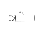
600 WGM共振器
612 光路
614 光路
Claims (20)
- 複数のモードファミリーを有するモノリシック共振器を提供するステップ;
前記複数のモードファミリーのうちの少なくとも第1のモードファミリーの品質を劣化させるように、前記共振器の一部分の屈折率を変更するステップ
を含む、方法。 - 前記モノリシック共振器は、ウィスパリングギャラリーモード共振器及び全内部反射共振器のうちの少なくとも1つを含む、請求項1に記載の方法。
- 前記複数のモードファミリーのうち、1つを除いて全てを排除するように、前記共振器の複数の部分の屈折率を変更するステップを更に含む、請求項1に記載の方法。
- 前記共振器の複数の部分の屈折率を変更する前記ステップは、前記複数のモードファミリーのうちの1つの場所に突出部を形成するステップを含む、請求項3に記載の方法。
- 前記複数のモードファミリーのうちのいずれも、互いに空間的に重ならない、請求項1に記載の方法。
- 前記共振器の前記一部分の屈折率を変更する前記ステップの前に、前記複数のモードファミリーのうち、劣化させる上記第1のモードファミリーを、ユーザが選択できるようにする、ユーザインタフェースを提示するステップを更に含む、請求項1に記載の方法。
- 屈折率を変更する前記ステップは、前記構造の前記一部分の表面に沿って少なくとも1つの窪みを形成するステップを含む、請求項1に記載の方法。
- 工具を用いて前記構造の前記一部分を引っ掻くことによって、前記少なくとも1つの窪みを形成するステップを更に含む、請求項7に記載の方法。
- 高温の物体を用いて前記構造の前記一部分を切除することによって、前記少なくとも1つの窪みを形成するステップを更に含む、請求項7に記載の方法。
- レーザビームを用いて前記構造の前記一部分を切除することによって、前記少なくとも1つのキャビティを形成するステップを更に含む、請求項7に記載の方法。
- 前記キャビティの幅は最大1ミクロンである、請求項7に記載の方法。
- 屈折率を変更する前記ステップは、腐食性化学物質を用いて前記構造の前記一部分をエッチングするステップを含む、請求項1に記載の方法。
- 屈折率を変更する前記ステップは、前記構造の前記一部分の表面の下に、局所的に改造された構造を形成するステップを含む、請求項1に記載の方法。
- 前記局所的に改造された構造は、レーザを用いて形成される、請求項13に記載の方法。
- 前記局所的に改造された構造は、放電を用いて形成される、請求項13に記載の方法。
- 屈折率を変更する前記ステップは、前記構造の前記一部分の前記表面の下に、複数のボイドを形成するステップを含む、請求項13に記載の方法。
- 前記ボイドは、水素イオン注入を用いて形成される、請求項13に記載の方法。
- 前記ボイドは、前記構造の最も近接した表面から最大5ミクロンの位置に形成される、請求項13に記載の方法。
- 前記ボイドは、前記構造の最も近接した表面から最大3ミクロンの位置に形成される、請求項13に記載の方法。
- 前記品質の劣化は、前記第1のモードの品質係数が少なくとも3桁低下することを含む、請求項1に記載の方法。
Applications Claiming Priority (1)
| Application Number | Priority Date | Filing Date | Title |
|---|---|---|---|
| PCT/US2014/024786 WO2015137945A1 (en) | 2014-03-12 | 2014-03-12 | Systems and methods for removing mode families |
Publications (2)
| Publication Number | Publication Date |
|---|---|
| JP2017509166A true JP2017509166A (ja) | 2017-03-30 |
| JP6476213B2 JP6476213B2 (ja) | 2019-02-27 |
Family
ID=50736139
Family Applications (1)
| Application Number | Title | Priority Date | Filing Date |
|---|---|---|---|
| JP2016575294A Expired - Fee Related JP6476213B2 (ja) | 2014-03-12 | 2014-03-12 | モードファミリーを除去するためのシステム及び方法 |
Country Status (4)
| Country | Link |
|---|---|
| JP (1) | JP6476213B2 (ja) |
| CN (1) | CN106463907A (ja) |
| DE (1) | DE112014006454T5 (ja) |
| WO (1) | WO2015137945A1 (ja) |
Cited By (1)
| Publication number | Priority date | Publication date | Assignee | Title |
|---|---|---|---|---|
| JP2023503782A (ja) * | 2019-09-30 | 2023-02-01 | ジーエム クルーズ ホールディングス エルエルシー | 局所的イオン注入空隙を有する光共振器 |
Citations (19)
| Publication number | Priority date | Publication date | Assignee | Title |
|---|---|---|---|---|
| JPS5163092A (ja) * | 1974-11-25 | 1976-06-01 | Agie Ag Ind Elektronik | Senjodenkyokuoshosuru hodenkakoki |
| JPH05206583A (ja) * | 1991-09-17 | 1993-08-13 | American Teleph & Telegr Co <Att> | ささやきモードマイクロ共振器 |
| WO2001093334A1 (en) * | 2000-05-30 | 2001-12-06 | Shin-Etsu Handotai Co.,Ltd. | Method for producing bonded wafer and bonded wafer |
| JP2002172528A (ja) * | 2000-12-06 | 2002-06-18 | Ind Technol Res Inst | ケミカルエッチング作用具備の複合放電加工法及び装置 |
| JP2002185064A (ja) * | 2000-10-10 | 2002-06-28 | Korea Advanced Inst Of Science & Technol | エバネッセント波微小共振器レーザー |
| JP2004503947A (ja) * | 2000-06-15 | 2004-02-05 | フラウンホッファー−ゲゼルシャフト ツァー フェーデルング デア アンゲバンテン フォルシュング エー ファー | モード選択性位相構造を有するレーザー共振器 |
| JP2004503816A (ja) * | 2000-06-15 | 2004-02-05 | カリフォルニア インスティテュート オブ テクノロジー | マイクロささやき回廊モード共振器における直接電気光変換及び光変調 |
| JP2005043699A (ja) * | 2003-07-23 | 2005-02-17 | Sony Corp | 液晶表示装置およびその製造方法 |
| JP2005183963A (ja) * | 2003-12-17 | 2005-07-07 | Palo Alto Research Center Inc | 格子アウトカップル型マイクロキャビティ・ディスク共振器及びその製造方法 |
| JP2006511841A (ja) * | 2002-12-18 | 2006-04-06 | ローズマウント インコーポレイテッド | チューニング可能な光学フィルタ |
| JP2006515081A (ja) * | 2003-02-03 | 2006-05-18 | カリフォルニア インスティテュート オブ テクノロジー | 電気光学ウィスパリングギャラリモード共振器を有する同調可能光フィルタ |
| JP2006267207A (ja) * | 2005-03-22 | 2006-10-05 | Nippon Telegr & Teleph Corp <Ntt> | 光共振器 |
| JP2007508714A (ja) * | 2003-10-14 | 2007-04-05 | スリーエム イノベイティブ プロパティズ カンパニー | ハイブリッド球−導波路共振器 |
| US7382808B1 (en) * | 2004-12-15 | 2008-06-03 | Hrl Laboratories, Llc | Apparatus and method for spatial mode selection of planar waveguide and thin slab lasers in the large cross section size direction |
| JP2009177154A (ja) * | 2007-12-27 | 2009-08-06 | Semiconductor Energy Lab Co Ltd | 半導体基板の作製方法、および半導体装置の作製方法 |
| JP2010530142A (ja) * | 2007-06-13 | 2010-09-02 | オーイーウェイブス,インコーポレーテッド | ウィスパリングギャラリーモード共振器に同期されるチューニング可能レーザ |
| JP2012185872A (ja) * | 2011-03-03 | 2012-09-27 | Hitachi Consumer Electronics Co Ltd | 情報記録再生装置 |
| US20120274944A1 (en) * | 2011-02-18 | 2012-11-01 | Muhammad Maqbool | Titanium-doped amorphous aluminum nitride microlaser device and method for making and using same |
| WO2012154209A1 (en) * | 2010-11-29 | 2012-11-15 | President And Fellows Of Harvard College | Highly unidirectional microcavity resonators |
-
2014
- 2014-03-12 CN CN201480079101.0A patent/CN106463907A/zh active Pending
- 2014-03-12 DE DE112014006454.8T patent/DE112014006454T5/de not_active Ceased
- 2014-03-12 JP JP2016575294A patent/JP6476213B2/ja not_active Expired - Fee Related
- 2014-03-12 WO PCT/US2014/024786 patent/WO2015137945A1/en not_active Ceased
Patent Citations (19)
| Publication number | Priority date | Publication date | Assignee | Title |
|---|---|---|---|---|
| JPS5163092A (ja) * | 1974-11-25 | 1976-06-01 | Agie Ag Ind Elektronik | Senjodenkyokuoshosuru hodenkakoki |
| JPH05206583A (ja) * | 1991-09-17 | 1993-08-13 | American Teleph & Telegr Co <Att> | ささやきモードマイクロ共振器 |
| WO2001093334A1 (en) * | 2000-05-30 | 2001-12-06 | Shin-Etsu Handotai Co.,Ltd. | Method for producing bonded wafer and bonded wafer |
| JP2004503947A (ja) * | 2000-06-15 | 2004-02-05 | フラウンホッファー−ゲゼルシャフト ツァー フェーデルング デア アンゲバンテン フォルシュング エー ファー | モード選択性位相構造を有するレーザー共振器 |
| JP2004503816A (ja) * | 2000-06-15 | 2004-02-05 | カリフォルニア インスティテュート オブ テクノロジー | マイクロささやき回廊モード共振器における直接電気光変換及び光変調 |
| JP2002185064A (ja) * | 2000-10-10 | 2002-06-28 | Korea Advanced Inst Of Science & Technol | エバネッセント波微小共振器レーザー |
| JP2002172528A (ja) * | 2000-12-06 | 2002-06-18 | Ind Technol Res Inst | ケミカルエッチング作用具備の複合放電加工法及び装置 |
| JP2006511841A (ja) * | 2002-12-18 | 2006-04-06 | ローズマウント インコーポレイテッド | チューニング可能な光学フィルタ |
| JP2006515081A (ja) * | 2003-02-03 | 2006-05-18 | カリフォルニア インスティテュート オブ テクノロジー | 電気光学ウィスパリングギャラリモード共振器を有する同調可能光フィルタ |
| JP2005043699A (ja) * | 2003-07-23 | 2005-02-17 | Sony Corp | 液晶表示装置およびその製造方法 |
| JP2007508714A (ja) * | 2003-10-14 | 2007-04-05 | スリーエム イノベイティブ プロパティズ カンパニー | ハイブリッド球−導波路共振器 |
| JP2005183963A (ja) * | 2003-12-17 | 2005-07-07 | Palo Alto Research Center Inc | 格子アウトカップル型マイクロキャビティ・ディスク共振器及びその製造方法 |
| US7382808B1 (en) * | 2004-12-15 | 2008-06-03 | Hrl Laboratories, Llc | Apparatus and method for spatial mode selection of planar waveguide and thin slab lasers in the large cross section size direction |
| JP2006267207A (ja) * | 2005-03-22 | 2006-10-05 | Nippon Telegr & Teleph Corp <Ntt> | 光共振器 |
| JP2010530142A (ja) * | 2007-06-13 | 2010-09-02 | オーイーウェイブス,インコーポレーテッド | ウィスパリングギャラリーモード共振器に同期されるチューニング可能レーザ |
| JP2009177154A (ja) * | 2007-12-27 | 2009-08-06 | Semiconductor Energy Lab Co Ltd | 半導体基板の作製方法、および半導体装置の作製方法 |
| WO2012154209A1 (en) * | 2010-11-29 | 2012-11-15 | President And Fellows Of Harvard College | Highly unidirectional microcavity resonators |
| US20120274944A1 (en) * | 2011-02-18 | 2012-11-01 | Muhammad Maqbool | Titanium-doped amorphous aluminum nitride microlaser device and method for making and using same |
| JP2012185872A (ja) * | 2011-03-03 | 2012-09-27 | Hitachi Consumer Electronics Co Ltd | 情報記録再生装置 |
Non-Patent Citations (2)
| Title |
|---|
| A. SHAW ET AL.: "Lasing properties of disk microcavity based on a circular Bragg reflector", APPLIED PHYSICS LETTERS, vol. 75, no. 20, JPN7017003894, 15 November 1999 (1999-11-15), US, pages 3051 - 3053, ISSN: 0003688333 * |
| MHER GHULINYAN ET AL.: "Monolithic whispering-gallery mode resonators with vertically coupled integrated bus waveguides", IEEE PHOTNNICS TECHNOLOGY LETTERS, vol. 23, no. 16, JPN7017003893, 15 August 2011 (2011-08-15), US, pages 1166 - 1168, ISSN: 0003688332 * |
Cited By (1)
| Publication number | Priority date | Publication date | Assignee | Title |
|---|---|---|---|---|
| JP2023503782A (ja) * | 2019-09-30 | 2023-02-01 | ジーエム クルーズ ホールディングス エルエルシー | 局所的イオン注入空隙を有する光共振器 |
Also Published As
| Publication number | Publication date |
|---|---|
| WO2015137945A1 (en) | 2015-09-17 |
| DE112014006454T5 (de) | 2016-11-24 |
| JP6476213B2 (ja) | 2019-02-27 |
| CN106463907A (zh) | 2017-02-22 |
Similar Documents
| Publication | Publication Date | Title |
|---|---|---|
| JP6986095B2 (ja) | 中空コアフォトニック結晶ファイバ及びこれを製造する方法 | |
| US6884960B2 (en) | Methods for creating optical structures in dielectrics using controlled energy deposition | |
| JP2019532004A (ja) | 非軸対称ビームスポットを用いて透明被加工物をレーザ加工するための装置及び方法 | |
| JP2019517134A (ja) | モノリシック可視波長ファイバーレーザー | |
| WO2017008022A1 (en) | Fiber with depressed central index for increased beam parameter product | |
| KR20150142920A (ko) | 펌프 광 제거기 및 그 제조 방법 | |
| US20200301059A1 (en) | A cutting element for use in a hair cutting device, and a method of manufacturing the same | |
| Tada et al. | Fabrication of high-Q microresonators using femtosecond laser micromachining | |
| EP3184232A1 (en) | Drilling device, method, and use | |
| JP6476213B2 (ja) | モードファミリーを除去するためのシステム及び方法 | |
| US20070263974A1 (en) | Laser Inscription of Optical Structures in Crystals | |
| US9403237B2 (en) | Systems and methods for removing mode families | |
| KR20090029278A (ko) | 파워 광섬유 레이저 장치 | |
| CN101409421A (zh) | 一种单模工作的大模场面积多模光纤激光器 | |
| US10693273B2 (en) | Reflector, fiber cavity, and fiber laser | |
| US20050167410A1 (en) | Methods for creating optical structures in dielectrics using controlled energy deposition | |
| KR20190048126A (ko) | 방사상 전파를 위한 광섬유 팁의 제조방법 | |
| JP5403647B2 (ja) | 光ファイバの端面処理方法および接続方法 | |
| JP2010107661A (ja) | レーザ光発生装置 | |
| JP2016161915A (ja) | 光導波路素子および光学デバイス | |
| Fujii et al. | Ultrahigh-Q crystalline microresonator fabricated with computer-controlled machining without polishing | |
| JP2006305580A (ja) | 線材の切断方法並びに線材の端面整形方法 | |
| JP2007071950A (ja) | ダブルクラッドホーリーファイバ、ファイバアンプ及びファイバレーザ | |
| Yun-Jun et al. | Narrow linewidth Tm3+-doped large core fiber laser based on a femtosecond written fiber Bragg grating | |
| MIZUMOTO et al. | Development of CaF2-brass hybrid WGM microcavity by using ultra-precision machining |
Legal Events
| Date | Code | Title | Description |
|---|---|---|---|
| A621 | Written request for application examination |
Free format text: JAPANESE INTERMEDIATE CODE: A621 Effective date: 20161221 |
|
| A977 | Report on retrieval |
Free format text: JAPANESE INTERMEDIATE CODE: A971007 Effective date: 20171117 |
|
| A131 | Notification of reasons for refusal |
Free format text: JAPANESE INTERMEDIATE CODE: A131 Effective date: 20171128 |
|
| A521 | Request for written amendment filed |
Free format text: JAPANESE INTERMEDIATE CODE: A523 Effective date: 20180223 |
|
| A131 | Notification of reasons for refusal |
Free format text: JAPANESE INTERMEDIATE CODE: A131 Effective date: 20180605 |
|
| TRDD | Decision of grant or rejection written | ||
| A01 | Written decision to grant a patent or to grant a registration (utility model) |
Free format text: JAPANESE INTERMEDIATE CODE: A01 Effective date: 20190115 |
|
| A61 | First payment of annual fees (during grant procedure) |
Free format text: JAPANESE INTERMEDIATE CODE: A61 Effective date: 20190204 |
|
| R150 | Certificate of patent or registration of utility model |
Ref document number: 6476213 Country of ref document: JP Free format text: JAPANESE INTERMEDIATE CODE: R150 |
|
| LAPS | Cancellation because of no payment of annual fees |