JP2017520906A - 貫通ガラスバイアの作製のための接合材料のエッチバックプロセス - Google Patents
貫通ガラスバイアの作製のための接合材料のエッチバックプロセス Download PDFInfo
- Publication number
- JP2017520906A JP2017520906A JP2016565202A JP2016565202A JP2017520906A JP 2017520906 A JP2017520906 A JP 2017520906A JP 2016565202 A JP2016565202 A JP 2016565202A JP 2016565202 A JP2016565202 A JP 2016565202A JP 2017520906 A JP2017520906 A JP 2017520906A
- Authority
- JP
- Japan
- Prior art keywords
- bonding layer
- substrate
- holes
- carrier
- vias
- Prior art date
- Legal status (The legal status is an assumption and is not a legal conclusion. Google has not performed a legal analysis and makes no representation as to the accuracy of the status listed.)
- Pending
Links
Images



Classifications
-
- C—CHEMISTRY; METALLURGY
- C03—GLASS; MINERAL OR SLAG WOOL
- C03C—CHEMICAL COMPOSITION OF GLASSES, GLAZES OR VITREOUS ENAMELS; SURFACE TREATMENT OF GLASS; SURFACE TREATMENT OF FIBRES OR FILAMENTS MADE FROM GLASS, MINERALS OR SLAGS; JOINING GLASS TO GLASS OR OTHER MATERIALS
- C03C15/00—Surface treatment of glass, not in the form of fibres or filaments, by etching
-
- H—ELECTRICITY
- H10—SEMICONDUCTOR DEVICES; ELECTRIC SOLID-STATE DEVICES NOT OTHERWISE PROVIDED FOR
- H10P—GENERIC PROCESSES OR APPARATUS FOR THE MANUFACTURE OR TREATMENT OF DEVICES COVERED BY CLASS H10
- H10P72/00—Handling or holding of wafers, substrates or devices during manufacture or treatment thereof
- H10P72/70—Handling or holding of wafers, substrates or devices during manufacture or treatment thereof for supporting or gripping
- H10P72/74—Handling or holding of wafers, substrates or devices during manufacture or treatment thereof for supporting or gripping using temporarily an auxiliary support
-
- H—ELECTRICITY
- H10—SEMICONDUCTOR DEVICES; ELECTRIC SOLID-STATE DEVICES NOT OTHERWISE PROVIDED FOR
- H10W—GENERIC PACKAGES, INTERCONNECTIONS, CONNECTORS OR OTHER CONSTRUCTIONAL DETAILS OF DEVICES COVERED BY CLASS H10
- H10W70/00—Package substrates; Interposers; Redistribution layers [RDL]
- H10W70/01—Manufacture or treatment
- H10W70/05—Manufacture or treatment of insulating or insulated package substrates, or of interposers, or of redistribution layers
- H10W70/095—Manufacture or treatment of insulating or insulated package substrates, or of interposers, or of redistribution layers of vias therein
-
- H—ELECTRICITY
- H10—SEMICONDUCTOR DEVICES; ELECTRIC SOLID-STATE DEVICES NOT OTHERWISE PROVIDED FOR
- H10W—GENERIC PACKAGES, INTERCONNECTIONS, CONNECTORS OR OTHER CONSTRUCTIONAL DETAILS OF DEVICES COVERED BY CLASS H10
- H10W70/00—Package substrates; Interposers; Redistribution layers [RDL]
- H10W70/60—Insulating or insulated package substrates; Interposers; Redistribution layers
- H10W70/62—Insulating or insulated package substrates; Interposers; Redistribution layers characterised by their interconnections
- H10W70/63—Vias, e.g. via plugs
- H10W70/635—Through-vias
-
- H—ELECTRICITY
- H10—SEMICONDUCTOR DEVICES; ELECTRIC SOLID-STATE DEVICES NOT OTHERWISE PROVIDED FOR
- H10W—GENERIC PACKAGES, INTERCONNECTIONS, CONNECTORS OR OTHER CONSTRUCTIONAL DETAILS OF DEVICES COVERED BY CLASS H10
- H10W70/00—Package substrates; Interposers; Redistribution layers [RDL]
- H10W70/60—Insulating or insulated package substrates; Interposers; Redistribution layers
- H10W70/62—Insulating or insulated package substrates; Interposers; Redistribution layers characterised by their interconnections
- H10W70/65—Shapes or dispositions of interconnections
-
- H—ELECTRICITY
- H10—SEMICONDUCTOR DEVICES; ELECTRIC SOLID-STATE DEVICES NOT OTHERWISE PROVIDED FOR
- H10W—GENERIC PACKAGES, INTERCONNECTIONS, CONNECTORS OR OTHER CONSTRUCTIONAL DETAILS OF DEVICES COVERED BY CLASS H10
- H10W70/00—Package substrates; Interposers; Redistribution layers [RDL]
- H10W70/60—Insulating or insulated package substrates; Interposers; Redistribution layers
- H10W70/62—Insulating or insulated package substrates; Interposers; Redistribution layers characterised by their interconnections
- H10W70/66—Conductive materials thereof
-
- H—ELECTRICITY
- H10—SEMICONDUCTOR DEVICES; ELECTRIC SOLID-STATE DEVICES NOT OTHERWISE PROVIDED FOR
- H10W—GENERIC PACKAGES, INTERCONNECTIONS, CONNECTORS OR OTHER CONSTRUCTIONAL DETAILS OF DEVICES COVERED BY CLASS H10
- H10W70/00—Package substrates; Interposers; Redistribution layers [RDL]
- H10W70/60—Insulating or insulated package substrates; Interposers; Redistribution layers
- H10W70/67—Insulating or insulated package substrates; Interposers; Redistribution layers characterised by their insulating layers or insulating parts
- H10W70/69—Insulating materials thereof
-
- H—ELECTRICITY
- H10—SEMICONDUCTOR DEVICES; ELECTRIC SOLID-STATE DEVICES NOT OTHERWISE PROVIDED FOR
- H10W—GENERIC PACKAGES, INTERCONNECTIONS, CONNECTORS OR OTHER CONSTRUCTIONAL DETAILS OF DEVICES COVERED BY CLASS H10
- H10W70/00—Package substrates; Interposers; Redistribution layers [RDL]
- H10W70/60—Insulating or insulated package substrates; Interposers; Redistribution layers
- H10W70/67—Insulating or insulated package substrates; Interposers; Redistribution layers characterised by their insulating layers or insulating parts
- H10W70/69—Insulating materials thereof
- H10W70/692—Ceramics or glasses
-
- H—ELECTRICITY
- H10—SEMICONDUCTOR DEVICES; ELECTRIC SOLID-STATE DEVICES NOT OTHERWISE PROVIDED FOR
- H10P—GENERIC PROCESSES OR APPARATUS FOR THE MANUFACTURE OR TREATMENT OF DEVICES COVERED BY CLASS H10
- H10P72/00—Handling or holding of wafers, substrates or devices during manufacture or treatment thereof
- H10P72/70—Handling or holding of wafers, substrates or devices during manufacture or treatment thereof for supporting or gripping
- H10P72/74—Handling or holding of wafers, substrates or devices during manufacture or treatment thereof for supporting or gripping using temporarily an auxiliary support
- H10P72/7412—Handling or holding of wafers, substrates or devices during manufacture or treatment thereof for supporting or gripping using temporarily an auxiliary support the auxiliary support including means facilitating the separation of a device or wafer from the auxiliary support
-
- H—ELECTRICITY
- H10—SEMICONDUCTOR DEVICES; ELECTRIC SOLID-STATE DEVICES NOT OTHERWISE PROVIDED FOR
- H10P—GENERIC PROCESSES OR APPARATUS FOR THE MANUFACTURE OR TREATMENT OF DEVICES COVERED BY CLASS H10
- H10P72/00—Handling or holding of wafers, substrates or devices during manufacture or treatment thereof
- H10P72/70—Handling or holding of wafers, substrates or devices during manufacture or treatment thereof for supporting or gripping
- H10P72/74—Handling or holding of wafers, substrates or devices during manufacture or treatment thereof for supporting or gripping using temporarily an auxiliary support
- H10P72/7424—Handling or holding of wafers, substrates or devices during manufacture or treatment thereof for supporting or gripping using temporarily an auxiliary support used as a support during the manufacture of self-supporting substrates
-
- H—ELECTRICITY
- H10—SEMICONDUCTOR DEVICES; ELECTRIC SOLID-STATE DEVICES NOT OTHERWISE PROVIDED FOR
- H10P—GENERIC PROCESSES OR APPARATUS FOR THE MANUFACTURE OR TREATMENT OF DEVICES COVERED BY CLASS H10
- H10P72/00—Handling or holding of wafers, substrates or devices during manufacture or treatment thereof
- H10P72/70—Handling or holding of wafers, substrates or devices during manufacture or treatment thereof for supporting or gripping
- H10P72/74—Handling or holding of wafers, substrates or devices during manufacture or treatment thereof for supporting or gripping using temporarily an auxiliary support
- H10P72/743—Handling or holding of wafers, substrates or devices during manufacture or treatment thereof for supporting or gripping using temporarily an auxiliary support used as a support during manufacture of interconnect decals or build up layers
-
- H—ELECTRICITY
- H10—SEMICONDUCTOR DEVICES; ELECTRIC SOLID-STATE DEVICES NOT OTHERWISE PROVIDED FOR
- H10P—GENERIC PROCESSES OR APPARATUS FOR THE MANUFACTURE OR TREATMENT OF DEVICES COVERED BY CLASS H10
- H10P72/00—Handling or holding of wafers, substrates or devices during manufacture or treatment thereof
- H10P72/70—Handling or holding of wafers, substrates or devices during manufacture or treatment thereof for supporting or gripping
- H10P72/74—Handling or holding of wafers, substrates or devices during manufacture or treatment thereof for supporting or gripping using temporarily an auxiliary support
- H10P72/744—Details of chemical or physical process used for separating the auxiliary support from a device or a wafer
Landscapes
- Chemical & Material Sciences (AREA)
- Engineering & Computer Science (AREA)
- Life Sciences & Earth Sciences (AREA)
- Chemical Kinetics & Catalysis (AREA)
- General Chemical & Material Sciences (AREA)
- Geochemistry & Mineralogy (AREA)
- Materials Engineering (AREA)
- Organic Chemistry (AREA)
- Internal Circuitry In Semiconductor Integrated Circuit Devices (AREA)
- Printing Elements For Providing Electric Connections Between Printed Circuits (AREA)
- Physics & Mathematics (AREA)
- Geometry (AREA)
- Surface Treatment Of Glass (AREA)
- Drying Of Semiconductors (AREA)
- Weting (AREA)
- Ceramic Engineering (AREA)
Abstract
Description
基板に複数のバイアを作製するための方法において、前記方法が、
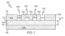
複数の孔を有する前記基板の第1の面をキャリアの第1の面に接合層によって接合する工程、前記接合層は前記基板の前記第1の面と前記キャリアの前記第1の面の間の厚さtを有し、前記複数の孔の内の少なくともいくつかに延び込んで、前記ガラス基板の前記第1の面からの高さhを有する接着剤プラグを形成する、
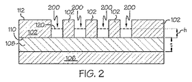
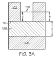
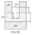
前記基板の前記複数の孔を通して前記接合層を深さdまでエッチングする工程、前記深さdは前記厚さtと前記高さhの和以下である、及び
前記複数の孔を、前記複数のバイアを形成するため、材料で埋め込む工程、
を含む、方法。
パルスレーザビームを用いて孔開けすることで前記基板に前記複数の孔を形成する工程をさらに含む、実施形態1に記載の方法。
前記接合層をエッチングする工程がウエットエッチングプロセスを利用する工程を含む、実施形態1または2に記載の方法。
前記接合層をエッチングする工程がドライエッチングプロセスを利用する工程を含む、実施形態1または2に記載の方法。
前記材料が前記接合層に長さlで延び込む導電材料であり、前記lは前記深さdと前記高さhの間の差に等しい、及び
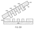
前記方法が前記複数のバイアを有する前記基板を前記接合層及び前記キャリアから剥離させる工程をさらに含み、前記複数のバイアを形成している前記導電材料の一部が前記基板の前記第1の面から突き出す、
実施形態1から4のいずれかに記載の方法。
前記深さdが前記接合層の厚さtと前記高さhの和に等しく、よって前記長さlが前記高さhに等しい、実施形態5に記載の方法。
基板に複数のバイアを作製するための方法において、前記方法が、
複数の孔を有する前記基板の第1の面をキャリアの第1の面に接合層によって接合する工程、前記接合層は前記基板の前記第1の面と前記キャリアの前記第1の面の間の厚さtを有する、
前記基板の前記複数の孔を通して前記接合層を、ウエットエッチングプロセスを用いて、深さdまでエッチングする工程、
前記複数の孔を、前記ガラスに前記複数のバイアを形成するため、導電材料で埋め込む工程、前記導電材料は前記接合層に長さlまで延び込み、前記長さlは前記厚さtより小さい、及び
前記複数のバイアを有する前記基板を前記接合層及び前記キャリアから剥離させる工程、前記導電材料は前記基板の前記第1の面から突き出す、
を含む、方法。
前記基板が100μm以下の厚さを有する、実施形態7に記載の方法。
前記基板の前記厚さが100μmより薄い、実施形態8に記載の方法。
前記ウエットエッチングプロセスが、HF及びアセトンから選ばれる溶剤に前記接合層をさらす工程を含む、実施形態7から9のいずれかに記載の方法。
前記基板が前記エッチングプロセスに対するハードマスクであるように、前記基板を通して前記接合層が前記溶剤にさらされる、実施形態10に記載の方法。
前記基板が100μm以下の厚さを有する、実施形態11に記載の方法。
前記導電材料が銅材料を含む、実施形態7から12のいずれかに記載の方法。
前記方法が前記複数のバイアを有する前記基板を三次元積層型集積回路に組み込む工程をさらに含む、実施形態7〜13に記載の方法。
基板に複数のバイアを作製するための方法において、前記方法が、
複数の孔を有する前記基板の第1の面をキャリアの第1の面に接合層を用いて接合する工程、前記接合層は前記基板の前記第1の面と前記キャリアの前記第1の面の間の厚さtを有する、
前記基板の前記複数の孔を通して前記接合層を、ドライエッチングプロセスを用いて、深さdまでエッチングする工程、前記深さdは前記基板の前記第1の面から前記接合層に前記エッチングが延び込んだ長さlと前記複数の孔の内の少なくともいくつかに前記接合層が延びこむことで形成された接着剤プラグの高さhの和に等しく、前記長さlは前記厚さtに等しく、前記キャリアの前記第1の面が前記ドライエッチングプロセスに対するストップ層である、
前記複数の孔を、前記基板に前記複数のバイアを形成するため、導電材料で埋め込む工程、前記導電材料は前記キャリアの前記第1の面まで前記接合層を貫通する、及び
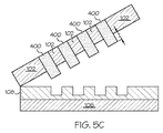
前記複数のバイアを有する前記基板を前記接合層及び前記キャリアから剥離させる工程、前記導電材料は前記ガラス基板の前記第1の面から長さlで延びるピラーを形成する、
を含む、方法。
前記ドライエッチングプロセスがO2またはアルゴンを含有するガスの内の少なくとも1つから発生されるプラズマに前記接合層をさらす工程を含む、実施形態15に記載の方法。
前記導電材料が銅を含む、実施形態15または16に記載の方法。
前記ピラーのそれぞれが、前記基板の第1の面に実質的に垂直な方向に延びる、前記基板の前記第1の面から延びる円筒を含む、実施形態15から17のいずれかに記載の方法。
前記基板が100μm以下の厚さを有する、実施形態15から18のいずれかに記載の方法。
前記基板の前記厚さが100μmより薄い、実施形態19に記載の方法
102 ガラス基板
104 孔
106 ガラスキャリア
108 接合層
110,112 ガラス基板の面
114,116 ガラスキャリアの面
118 接着剤プラグ
120 接着剤プラグの遠位面
200 エッチャント
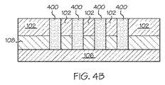
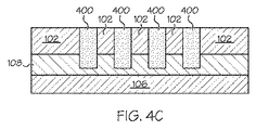
400 バイア/導電材料
Claims (10)
- 基板に複数のバイアを作製するための方法において、前記方法が、
複数の孔を有する前記基板の第1の面をキャリアの第1の面に接合層によって接合する工程、前記接合層は前記基板の前記第1の面と前記キャリアの前記第1の面の間の厚さtを有し、前記複数の孔の内の少なくともいくつかに延び込んで、前記ガラス基板の前記第1の面からの高さhを有する接着剤プラグを形成する、
前記基板の前記複数の孔を通して前記接合層を深さdまでエッチングする工程、前記深さdは前記厚さtと前記高さhの和以下である、及び
前記複数の孔を、前記複数のバイアを形成するため、材料で埋め込む工程、
を含むことを特徴とする方法。 - 前記接合層をエッチングする工程がウエットエッチングプロセスを利用する工程を含むことを特徴とする請求項1に記載の方法。
- 前記接合層をエッチングする工程がドライエッチングプロセスを利用する工程を含むことを特徴とする請求項1に記載の方法。
- 前記材料が前記接合層に長さlで延び込む導電材料であり、前記lは前記深さdと前記高さhの間の差に等しい、及び
前記方法が前記複数のバイアを有する前記基板を前記接合層及び前記キャリアから剥離させる工程をさらに含み、前記複数のバイアを形成している前記導電材料の一部が前記基板の前記第1の面から突き出す、
ことを特徴とする請求項1から3のいずれかに記載の方法。 - 基板に複数のバイアを作製するための方法において、前記方法が、
複数の孔を有する前記基板の第1の面をキャリアの第1の面に接合層によって接合する工程、前記接合層は前記基板の前記第1の面と前記キャリアの前記第1の面の間の厚さtを有する、
前記基板の前記複数の孔を通して前記接合層を、ウエットエッチングプロセスを用いて、深さdまでエッチングする工程、
前記複数の孔を、前記ガラスに前記複数のバイアを形成するため、導電材料で埋め込む工程、前記導電材料は前記接合層に長さlまで延び込み、前記長さlは前記厚さtより小さい、及び
前記複数のバイアを有する前記基板を前記接合層及び前記キャリアから剥離させる工程、前記導電材料は前記基板の前記第1の面から突き出す、
を含むことを特徴とする方法。 - 前記基板が100μm以下の厚さを有することを特徴とする請求項5に記載の方法。
- 前記ウエットエッチングプロセスがHF及びアセトンから選ばれる溶剤に前記接合層をさらす工程を含むことを特徴とする請求項5または6に記載の方法。
- 前記基板が前記エッチングプロセスに対するハードマスクであるように前記基板を通して前記接合層が前記溶剤にさらされることを特徴とする請求項7に記載の方法。
- 基板に複数のバイアを作製するための方法において、前記方法が、
複数の孔を有する前記基板の第1の面をキャリアの第1の面に接合層を用いて接合する工程、前記接合層は前記基板の前記第1の面と前記キャリアの前記第1の面の間の厚さtを有する、
前記基板の前記複数の孔を通して前記接合層を、ドライエッチングプロセスを用いて、深さdまでエッチングする工程、前記深さdは前記基板の前記第1の面から前記接合層に前記エッチングが延び込んだ長さlと前記複数の孔の内の少なくともいくつかに前記接合層が延びこむことで形成された接着剤プラグの高さhの和に等しく、前記長さlは前記厚さtに等しく、前記キャリアの前記第1の面が前記ドライエッチングプロセスに対するストップ層である、
前記複数の孔を、前記基板に前記複数のバイアを形成するため、導電材料で埋め込む工程、前記導電材料は前記キャリアの前記第1の面まで前記接合層を貫通する、及び
前記複数のバイアを有する前記基板を前記接合層及び前記キャリアから剥離させる工程、前記導電材料は前記ガラス基板の前記第1の面から長さlで延びるピラーを形成する、
を含むことを特徴とする方法。 - 前記ドライエッチングプロセスがO2またはアルゴンを含有するガスの内の少なくとも1つから発生されるプラズマに前記接合層をさらす工程を含むことを特徴とする請求項9に記載の方法。
Applications Claiming Priority (3)
| Application Number | Priority Date | Filing Date | Title |
|---|---|---|---|
| US201461986370P | 2014-04-30 | 2014-04-30 | |
| US61/986,370 | 2014-04-30 | ||
| PCT/US2015/028200 WO2015168236A1 (en) | 2014-04-30 | 2015-04-29 | Etch back processes of bonding material for the manufacture of through-glass vias |
Publications (2)
| Publication Number | Publication Date |
|---|---|
| JP2017520906A true JP2017520906A (ja) | 2017-07-27 |
| JP2017520906A5 JP2017520906A5 (ja) | 2018-06-14 |
Family
ID=53177892
Family Applications (1)
| Application Number | Title | Priority Date | Filing Date |
|---|---|---|---|
| JP2016565202A Pending JP2017520906A (ja) | 2014-04-30 | 2015-04-29 | 貫通ガラスバイアの作製のための接合材料のエッチバックプロセス |
Country Status (7)
| Country | Link |
|---|---|
| US (2) | US9263300B2 (ja) |
| EP (1) | EP3138120B1 (ja) |
| JP (1) | JP2017520906A (ja) |
| KR (1) | KR20160145801A (ja) |
| CN (1) | CN106470953B (ja) |
| TW (1) | TWI659002B (ja) |
| WO (1) | WO2015168236A1 (ja) |
Families Citing this family (15)
| Publication number | Priority date | Publication date | Assignee | Title |
|---|---|---|---|---|
| WO2015168236A1 (en) * | 2014-04-30 | 2015-11-05 | Corning Incorporated | Etch back processes of bonding material for the manufacture of through-glass vias |
| US10410883B2 (en) | 2016-06-01 | 2019-09-10 | Corning Incorporated | Articles and methods of forming vias in substrates |
| US10794679B2 (en) | 2016-06-29 | 2020-10-06 | Corning Incorporated | Method and system for measuring geometric parameters of through holes |
| US10134657B2 (en) | 2016-06-29 | 2018-11-20 | Corning Incorporated | Inorganic wafer having through-holes attached to semiconductor wafer |
| TWI776825B (zh) * | 2016-11-18 | 2022-09-11 | 美商山姆科技公司 | 填充基板的穿通孔之填充材料及方法 |
| CN108231646A (zh) * | 2016-12-13 | 2018-06-29 | 中芯国际集成电路制造(上海)有限公司 | 一种半导体器件的制造方法 |
| US10580725B2 (en) | 2017-05-25 | 2020-03-03 | Corning Incorporated | Articles having vias with geometry attributes and methods for fabricating the same |
| US11078112B2 (en) | 2017-05-25 | 2021-08-03 | Corning Incorporated | Silica-containing substrates with vias having an axially variable sidewall taper and methods for forming the same |
| US12180108B2 (en) | 2017-12-19 | 2024-12-31 | Corning Incorporated | Methods for etching vias in glass-based articles employing positive charge organic molecules |
| US11554984B2 (en) | 2018-02-22 | 2023-01-17 | Corning Incorporated | Alkali-free borosilicate glasses with low post-HF etch roughness |
| TWI769376B (zh) | 2018-03-30 | 2022-07-01 | 美商山姆科技公司 | 導電性通孔及其製造方法 |
| US11148935B2 (en) | 2019-02-22 | 2021-10-19 | Menlo Microsystems, Inc. | Full symmetric multi-throw switch using conformal pinched through via |
| WO2021167787A1 (en) * | 2020-02-18 | 2021-08-26 | Corning Incorporated | Etching of glass surfaces to reduce electrostatic charging during processing |
| US11856711B2 (en) * | 2020-10-28 | 2023-12-26 | Infineon Technologies Austria Ag | Rogowski coil integrated in glass substrate |
| CN117747504B (zh) * | 2023-12-20 | 2024-07-19 | 西安赛富乐斯半导体科技有限公司 | 粘合胶层厚度调整方法 |
Citations (6)
| Publication number | Priority date | Publication date | Assignee | Title |
|---|---|---|---|---|
| JP2006161124A (ja) * | 2004-12-09 | 2006-06-22 | Canon Inc | 貫通電極の形成方法 |
| JP2007042741A (ja) * | 2005-08-01 | 2007-02-15 | Shinko Electric Ind Co Ltd | 電子部品実装構造体及びその製造方法 |
| JP2007067031A (ja) * | 2005-08-30 | 2007-03-15 | Tdk Corp | 配線基板の製造方法 |
| JP2012028533A (ja) * | 2010-07-22 | 2012-02-09 | Canon Inc | 基板貫通孔内への金属充填方法及び基板 |
| WO2013008344A1 (ja) * | 2011-07-14 | 2013-01-17 | 株式会社島津製作所 | プラズマ処理装置 |
| WO2014038326A1 (ja) * | 2012-09-07 | 2014-03-13 | 旭硝子株式会社 | インターポーザ用の中間品を製造する方法およびインターポーザ用の中間品 |
Family Cites Families (11)
| Publication number | Priority date | Publication date | Assignee | Title |
|---|---|---|---|---|
| US7425507B2 (en) | 2005-06-28 | 2008-09-16 | Micron Technology, Inc. | Semiconductor substrates including vias of nonuniform cross section, methods of forming and associated structures |
| US7429529B2 (en) * | 2005-08-05 | 2008-09-30 | Farnworth Warren M | Methods of forming through-wafer interconnects and structures resulting therefrom |
| US8455357B2 (en) * | 2008-10-10 | 2013-06-04 | Taiwan Semiconductor Manufacturing Co., Ltd. | Method of plating through wafer vias in a wafer for 3D packaging |
| JP5201048B2 (ja) * | 2009-03-25 | 2013-06-05 | 富士通株式会社 | 半導体装置とその製造方法 |
| US20110229687A1 (en) | 2010-03-19 | 2011-09-22 | Qualcomm Incorporated | Through Glass Via Manufacturing Process |
| US8411459B2 (en) | 2010-06-10 | 2013-04-02 | Taiwan Semiconductor Manufacturing Company, Ltd | Interposer-on-glass package structures |
| TWI599429B (zh) | 2010-11-30 | 2017-09-21 | 康寧公司 | 在玻璃中形成高密度孔洞陣列的方法 |
| TWI547454B (zh) | 2011-05-31 | 2016-09-01 | 康寧公司 | 於玻璃中高速製造微孔洞的方法 |
| CN105228788A (zh) | 2012-11-29 | 2016-01-06 | 康宁股份有限公司 | 用于激光钻孔基材的牺牲覆盖层及其方法 |
| US9425125B2 (en) * | 2014-02-20 | 2016-08-23 | Altera Corporation | Silicon-glass hybrid interposer circuitry |
| WO2015168236A1 (en) * | 2014-04-30 | 2015-11-05 | Corning Incorporated | Etch back processes of bonding material for the manufacture of through-glass vias |
-
2015
- 2015-04-29 WO PCT/US2015/028200 patent/WO2015168236A1/en not_active Ceased
- 2015-04-29 US US14/699,393 patent/US9263300B2/en not_active Expired - Fee Related
- 2015-04-29 JP JP2016565202A patent/JP2017520906A/ja active Pending
- 2015-04-29 CN CN201580036200.5A patent/CN106470953B/zh not_active Expired - Fee Related
- 2015-04-29 KR KR1020167032591A patent/KR20160145801A/ko not_active Withdrawn
- 2015-04-29 EP EP15722629.1A patent/EP3138120B1/en not_active Not-in-force
- 2015-04-30 TW TW104113956A patent/TWI659002B/zh not_active IP Right Cessation
-
2016
- 2016-02-02 US US15/013,241 patent/US20160155696A1/en not_active Abandoned
Patent Citations (6)
| Publication number | Priority date | Publication date | Assignee | Title |
|---|---|---|---|---|
| JP2006161124A (ja) * | 2004-12-09 | 2006-06-22 | Canon Inc | 貫通電極の形成方法 |
| JP2007042741A (ja) * | 2005-08-01 | 2007-02-15 | Shinko Electric Ind Co Ltd | 電子部品実装構造体及びその製造方法 |
| JP2007067031A (ja) * | 2005-08-30 | 2007-03-15 | Tdk Corp | 配線基板の製造方法 |
| JP2012028533A (ja) * | 2010-07-22 | 2012-02-09 | Canon Inc | 基板貫通孔内への金属充填方法及び基板 |
| WO2013008344A1 (ja) * | 2011-07-14 | 2013-01-17 | 株式会社島津製作所 | プラズマ処理装置 |
| WO2014038326A1 (ja) * | 2012-09-07 | 2014-03-13 | 旭硝子株式会社 | インターポーザ用の中間品を製造する方法およびインターポーザ用の中間品 |
Also Published As
| Publication number | Publication date |
|---|---|
| CN106470953B (zh) | 2019-03-12 |
| WO2015168236A1 (en) | 2015-11-05 |
| EP3138120B1 (en) | 2018-04-18 |
| US9263300B2 (en) | 2016-02-16 |
| EP3138120A1 (en) | 2017-03-08 |
| CN106470953A (zh) | 2017-03-01 |
| TWI659002B (zh) | 2019-05-11 |
| TW201600484A (zh) | 2016-01-01 |
| KR20160145801A (ko) | 2016-12-20 |
| US20150318187A1 (en) | 2015-11-05 |
| US20160155696A1 (en) | 2016-06-02 |
Similar Documents
| Publication | Publication Date | Title |
|---|---|---|
| US9263300B2 (en) | Etch back processes of bonding material for the manufacture of through-glass vias | |
| US20160079149A1 (en) | Wiring board provided with through electrode, method for manufacturing same and semiconductor device | |
| JP2006121053A (ja) | 電子部品のための薄いガラスチップ及びその製造方法 | |
| CN111903196A (zh) | 玻璃芯器件及其制造方法 | |
| JP2004158705A (ja) | 微細孔への金属充填方法及びその方法により形成された金属が充填した微細孔を備えたワーク | |
| CN102067289A (zh) | 多段型衬底的制造方法 | |
| JP2017520906A5 (ja) | ||
| CN107567651B (zh) | 具有贯通电极的布线基板及其制造方法 | |
| TWI689630B (zh) | 底部向上電解質通孔鍍覆方法 | |
| US9859159B2 (en) | Interconnection structure and manufacturing method thereof | |
| TWI461122B (zh) | 電路板及其製造方法 | |
| US10269585B2 (en) | Method of forming substrates with a through via | |
| JP6585526B2 (ja) | 配線基板の製造方法 | |
| TWI607678B (zh) | 中介層結構及其製作方法 | |
| JP2005093954A (ja) | 貫通電極付き基板、その製造方法及び電子デバイス | |
| KR20230081779A (ko) | 전기도금 층을 포함하는 비아들 및 비아들의 제조 방법들 | |
| CN106129026A (zh) | 半导体结构及其制作方法 | |
| JP2005039078A (ja) | 薄板基板構造形成用ウエーハ基板、この製造方法およびmems素子の製造方法 | |
| JP6492286B2 (ja) | 素子チップの製造方法 | |
| JP6180162B2 (ja) | 基板の貼り合わせ方法および貼り合わせ基板 | |
| CN106560916A (zh) | 元件芯片的制造方法以及元件芯片 | |
| JP2017118053A (ja) | パッケージ基板及びその製造方法 | |
| KR102819751B1 (ko) | 용융 본딩 및 본딩 분리를 위한 저밀도 실리콘 산화물에 대한 방법 및 구조물 | |
| JP2009111433A (ja) | 貫通電極付き半導体基板の製造方法、貫通電極付き半導体デバイスの製造方法 | |
| JP2019153902A (ja) | 複合基板の製造方法 |
Legal Events
| Date | Code | Title | Description |
|---|---|---|---|
| A521 | Request for written amendment filed |
Free format text: JAPANESE INTERMEDIATE CODE: A523 Effective date: 20180419 |
|
| A621 | Written request for application examination |
Free format text: JAPANESE INTERMEDIATE CODE: A621 Effective date: 20180419 |
|
| A521 | Request for written amendment filed |
Free format text: JAPANESE INTERMEDIATE CODE: A523 Effective date: 20180713 |
|
| A131 | Notification of reasons for refusal |
Free format text: JAPANESE INTERMEDIATE CODE: A131 Effective date: 20190417 |
|
| A601 | Written request for extension of time |
Free format text: JAPANESE INTERMEDIATE CODE: A601 Effective date: 20190717 |
|
| A02 | Decision of refusal |
Free format text: JAPANESE INTERMEDIATE CODE: A02 Effective date: 20190807 |