JP2017520935A - 伝送線路ビア構造 - Google Patents
伝送線路ビア構造 Download PDFInfo
- Publication number
- JP2017520935A JP2017520935A JP2017512633A JP2017512633A JP2017520935A JP 2017520935 A JP2017520935 A JP 2017520935A JP 2017512633 A JP2017512633 A JP 2017512633A JP 2017512633 A JP2017512633 A JP 2017512633A JP 2017520935 A JP2017520935 A JP 2017520935A
- Authority
- JP
- Japan
- Prior art keywords
- conductor portion
- transmission line
- substructures
- outer conductor
- support member
- Prior art date
- Legal status (The legal status is an assumption and is not a legal conclusion. Google has not performed a legal analysis and makes no representation as to the accuracy of the status listed.)
- Granted
Links
Images





Classifications
-
- H—ELECTRICITY
- H10—SEMICONDUCTOR DEVICES; ELECTRIC SOLID-STATE DEVICES NOT OTHERWISE PROVIDED FOR
- H10W—GENERIC PACKAGES, INTERCONNECTIONS, CONNECTORS OR OTHER CONSTRUCTIONAL DETAILS OF DEVICES COVERED BY CLASS H10
- H10W44/00—Electrical arrangements for controlling or matching impedance
- H10W44/20—Electrical arrangements for controlling or matching impedance at high-frequency [HF] or radio frequency [RF]
-
- H—ELECTRICITY
- H05—ELECTRIC TECHNIQUES NOT OTHERWISE PROVIDED FOR
- H05K—PRINTED CIRCUITS; CASINGS OR CONSTRUCTIONAL DETAILS OF ELECTRIC APPARATUS; MANUFACTURE OF ASSEMBLAGES OF ELECTRICAL COMPONENTS
- H05K1/00—Printed circuits
- H05K1/02—Details
- H05K1/0213—Electrical arrangements not otherwise provided for
- H05K1/0216—Reduction of cross-talk, noise or electromagnetic interference
- H05K1/0218—Reduction of cross-talk, noise or electromagnetic interference by printed shielding conductors, ground planes or power plane
- H05K1/0219—Printed shielding conductors for shielding around or between signal conductors, e.g. coplanar or coaxial printed shielding conductors
- H05K1/0222—Printed shielding conductors for shielding around or between signal conductors, e.g. coplanar or coaxial printed shielding conductors for shielding around a single via or around a group of vias, e.g. coaxial vias or vias surrounded by a grounded via fence
-
- H—ELECTRICITY
- H05—ELECTRIC TECHNIQUES NOT OTHERWISE PROVIDED FOR
- H05K—PRINTED CIRCUITS; CASINGS OR CONSTRUCTIONAL DETAILS OF ELECTRIC APPARATUS; MANUFACTURE OF ASSEMBLAGES OF ELECTRICAL COMPONENTS
- H05K1/00—Printed circuits
- H05K1/02—Details
- H05K1/0213—Electrical arrangements not otherwise provided for
- H05K1/0237—High frequency adaptations
- H05K1/025—Impedance arrangements, e.g. impedance matching, reduction of parasitic impedance
- H05K1/0251—Impedance arrangements, e.g. impedance matching, reduction of parasitic impedance related to vias or transitions between vias and transmission lines
-
- H—ELECTRICITY
- H10—SEMICONDUCTOR DEVICES; ELECTRIC SOLID-STATE DEVICES NOT OTHERWISE PROVIDED FOR
- H10W—GENERIC PACKAGES, INTERCONNECTIONS, CONNECTORS OR OTHER CONSTRUCTIONAL DETAILS OF DEVICES COVERED BY CLASS H10
- H10W20/00—Interconnections in chips, wafers or substrates
- H10W20/01—Manufacture or treatment
- H10W20/031—Manufacture or treatment of conductive parts of the interconnections
- H10W20/056—Manufacture or treatment of conductive parts of the interconnections by filling conductive material into holes, grooves or trenches
-
- H—ELECTRICITY
- H05—ELECTRIC TECHNIQUES NOT OTHERWISE PROVIDED FOR
- H05K—PRINTED CIRCUITS; CASINGS OR CONSTRUCTIONAL DETAILS OF ELECTRIC APPARATUS; MANUFACTURE OF ASSEMBLAGES OF ELECTRICAL COMPONENTS
- H05K1/00—Printed circuits
- H05K1/02—Details
- H05K1/11—Printed elements for providing electric connections to or between printed circuits
- H05K1/115—Via connections; Lands around holes or via connections
- H05K1/116—Lands, clearance holes or other lay-out details concerning the surrounding of a via
-
- H—ELECTRICITY
- H05—ELECTRIC TECHNIQUES NOT OTHERWISE PROVIDED FOR
- H05K—PRINTED CIRCUITS; CASINGS OR CONSTRUCTIONAL DETAILS OF ELECTRIC APPARATUS; MANUFACTURE OF ASSEMBLAGES OF ELECTRICAL COMPONENTS
- H05K2201/00—Indexing scheme relating to printed circuits covered by H05K1/00
- H05K2201/09—Shape and layout
- H05K2201/09209—Shape and layout details of conductors
- H05K2201/09654—Shape and layout details of conductors covering at least two types of conductors provided for in H05K2201/09218 - H05K2201/095
- H05K2201/09809—Coaxial layout
-
- H—ELECTRICITY
- H05—ELECTRIC TECHNIQUES NOT OTHERWISE PROVIDED FOR
- H05K—PRINTED CIRCUITS; CASINGS OR CONSTRUCTIONAL DETAILS OF ELECTRIC APPARATUS; MANUFACTURE OF ASSEMBLAGES OF ELECTRICAL COMPONENTS
- H05K2203/00—Indexing scheme relating to apparatus or processes for manufacturing printed circuits covered by H05K3/00
- H05K2203/30—Details of processes not otherwise provided for in H05K2203/01 - H05K2203/17
- H05K2203/308—Sacrificial means, e.g. for temporarily filling a space for making a via or a cavity or for making rigid-flexible PCBs
-
- H—ELECTRICITY
- H05—ELECTRIC TECHNIQUES NOT OTHERWISE PROVIDED FOR
- H05K—PRINTED CIRCUITS; CASINGS OR CONSTRUCTIONAL DETAILS OF ELECTRIC APPARATUS; MANUFACTURE OF ASSEMBLAGES OF ELECTRICAL COMPONENTS
- H05K3/00—Apparatus or processes for manufacturing printed circuits
- H05K3/40—Forming printed elements for providing electric connections to or between printed circuits
- H05K3/4038—Through-connections; Vertical interconnect access [VIA] connections
- H05K3/4046—Through-connections; Vertical interconnect access [VIA] connections using auxiliary conductive elements, e.g. metallic spheres, eyelets, pieces of wire
-
- H—ELECTRICITY
- H05—ELECTRIC TECHNIQUES NOT OTHERWISE PROVIDED FOR
- H05K—PRINTED CIRCUITS; CASINGS OR CONSTRUCTIONAL DETAILS OF ELECTRIC APPARATUS; MANUFACTURE OF ASSEMBLAGES OF ELECTRICAL COMPONENTS
- H05K3/00—Apparatus or processes for manufacturing printed circuits
- H05K3/40—Forming printed elements for providing electric connections to or between printed circuits
- H05K3/42—Plated through-holes or plated via connections
- H05K3/423—Plated through-holes or plated via connections characterised by electroplating method
- H05K3/424—Plated through-holes or plated via connections characterised by electroplating method by direct electroplating
-
- H—ELECTRICITY
- H10—SEMICONDUCTOR DEVICES; ELECTRIC SOLID-STATE DEVICES NOT OTHERWISE PROVIDED FOR
- H10W—GENERIC PACKAGES, INTERCONNECTIONS, CONNECTORS OR OTHER CONSTRUCTIONAL DETAILS OF DEVICES COVERED BY CLASS H10
- H10W44/00—Electrical arrangements for controlling or matching impedance
- H10W44/20—Electrical arrangements for controlling or matching impedance at high-frequency [HF] or radio frequency [RF]
- H10W44/203—Electrical connections
- H10W44/209—Vertical interconnections, e.g. vias
-
- H—ELECTRICITY
- H10—SEMICONDUCTOR DEVICES; ELECTRIC SOLID-STATE DEVICES NOT OTHERWISE PROVIDED FOR
- H10W—GENERIC PACKAGES, INTERCONNECTIONS, CONNECTORS OR OTHER CONSTRUCTIONAL DETAILS OF DEVICES COVERED BY CLASS H10
- H10W44/00—Electrical arrangements for controlling or matching impedance
- H10W44/20—Electrical arrangements for controlling or matching impedance at high-frequency [HF] or radio frequency [RF]
- H10W44/203—Electrical connections
- H10W44/209—Vertical interconnections, e.g. vias
- H10W44/212—Coaxial feed-throughs in substrates
Landscapes
- Engineering & Computer Science (AREA)
- Microelectronics & Electronic Packaging (AREA)
- Physics & Mathematics (AREA)
- Electromagnetism (AREA)
- Manufacturing & Machinery (AREA)
- Production Of Multi-Layered Print Wiring Board (AREA)
- Printing Elements For Providing Electric Connections Between Printed Circuits (AREA)
- Internal Circuitry In Semiconductor Integrated Circuit Devices (AREA)
- Structure Of Printed Boards (AREA)
Abstract
Description
本開示は一般に半導体デバイスおよびプロセスに関し、特に、半導体デバイス内の伝送線路ビア構造に関する。
いくつかの電子デバイスは、それらの波特性が考慮されなければならず、プリント回路基板(PCB)上の線路の長さまたは配線の長さが無視できない、十分に高い周波数を有する信号を用いる。そのように高い周波数の信号を伝播するために、PCBは伝送線路トレースを電子部品間に含む。伝送線路トレースをPCBの1つの側から別の側へと導くために、伝送線路ビアは、伝送線路と一致するインピーダンスを有することが必要である。1つの種類の伝送線路ビアは、中心信号導体をその間の固体誘電体で囲む外側グランド導体を有する同軸のビアである。
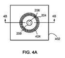
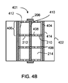
1つの例では、基板内の伝送線路ビア構造が、説明される。伝送線路ビア構造は、基板を通るビア内に、その長手軸に沿って積層された複数のサブ構造を含む。サブ構造の各々は中心導体部、外側導体部、および少なくとも1つの誘電体支持部材を含む。中心導体部は、長手軸に沿って延びる。外側導体部は、中心導体部の周りに配置される。誘電体支持部材(複数可)は、外側導体部および中心導体部を分離し、非固体容積を外側導体部と中心導体部との間に提供する。導電ペーストは、外側導体および中心導体を形成するために、複数のサブ構造のうちの連続するものの中心導体部および外側導体部の間に配置される。
上記の構造および方法が詳細に理解されることができるように、より具体的な説明が具体例を参照することによって行われ、そのいくつかは、添付された図面に図示されるだろう。しかし、留意すべきは、添付された図面は、純粋に本質的に例示的であり、そのためその特許請求の範囲を限定するものではなく、発明は他の均等に有効な実施形態を認めうる。
伝送線路ビア構造が、説明される。1つの例では、プリント回路基板(PCB)といった基板内に、同軸のビア構造が形成される。同軸のビア構造は、中心導体の周りに配置される外側導体を含む。1つまたは複数の誘電体支持部材は、ビア内に、中心導体を支持し、かつ、中心導体を外側導体から分離するために配置される。いずれの固体材料も、誘電体支持部材間にビアの長手軸に沿って配置されない。むしろ、誘電体支持部材間の容積は、空気で充填される。誘電体支持部材は、誘電体構造が実質的に空気であるように作られることができる。実質的に空気ベースの誘電体を使用することは、固体誘電体伝送線路ビアと比べて削減された大きさのビアを可能とする。これは、PCBの経路形成を向上させPCBの面積を浪費させないことができる。
Claims (14)
- 基板内の伝送線路ビア構造であって、
前記基板を通るビア内に、その長手軸に沿って積層された複数のサブ構造を備え、前記サブ構造の各々は、
前記長手軸に沿って延びる中心導体部と、
前記中心導体部の周りに配置される外側導体部と、
前記外側導体部と前記中心導体部とを分離し、前記外側導体部と前記中心導体部との間に非固体容積を提供する少なくとも1つの誘電体支持部材とを含み、前記伝送線路ビア構造はさらに、
外側導体および中心導体を形成するために、前記複数のサブ構造のうちの連続するものの前記中心導体部と外側導体部との間に配置される導電ペーストを備える、伝送線路ビア構造。 - 前記少なくとも1つの誘電体支持部材によって占有されない前記非固体容積の一部は、空気によって占有される、請求項1に記載の伝送線路ビア構造。
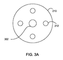
- 前記少なくとも1つの誘電体支持部材の各々は、誘電体材料のディスクを備え、前記誘電体材料のディスクは、そこを通る複数のボアを有する、請求項1または2に記載の伝送線路ビア構造。
- 前記少なくとも1つの誘電体支持部材の各々について、前記外側導体部に接触する前記ディスクのエッジは、前記ディスクの内側部分よりも厚い、請求項3に記載の伝送線路ビア構造。
- 前記基板内の前記ビアは、前記複数のサブ構造を囲む導体でメッキされている、請求項1から4のいずれか1項に記載の伝送線路ビア構造。
- 前記中心導体の長さと前記中心導体の直径との間の比は、30:1よりも大きい、請求項1〜5のいずれか1項に記載の伝送線路ビア構造。
- 前記中心導体および外側導体は、前記基板の少なくとも1つの表面上の少なくとも1つの伝送線路に結合される、請求項1〜6のいずれか1項に記載の伝送線路ビア構造。
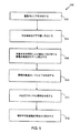
- 基板内の伝送線路ビア構造を形成する方法であって、
前記基板内に長手軸に沿ってその頂部表面と底部表面との間に延びるビアを形成することと、
複数のサブ構造を形成することを備え、前記複数のサブ構造の各々は、誘電体支持部材によって中心導体部から分離される外側導体部を含み、かつ前記誘電体支持部材間に犠牲材料を含み、前記方法はさらに、
外側導体および中心導体を形成するために、前記誘電体サブ構造のうちの連続するものの前記外側導体部および前記中心導体部の間に、導電ペーストで前記ビア内に前記複数のサブ構造を積層することと、
前記犠牲材料を前記複数のサブ構造の各々から除去し、非固体容積を前記中心導体部と前記外側導体部との間に提供することと、を備える方法。 - 前記誘電体支持部材は、そこを通るボアを有し、前記犠牲材料は、前記ボアを通して除去される、請求項8に記載の方法。
- 誘電体支持部材によって占有されない前記非固体容積の一部は、空気によって占有される、請求項8または9に記載の方法。
- 前記犠牲材料は、前記積層するステップの前に前記複数のサブ構造の各々から除去される、請求項8〜10のいずれか1項に記載の方法。
- 前記犠牲材料は、前記積層するステップの後に前記複数のサブ構造の各々から除去される、請求項8〜10のいずれか1項に記載の方法。
- 前記中心導体の長さと直径との間の比は30:1よりも大きい、請求項8〜12のいずれか1項に記載の方法。
- 前記複数のサブ構造の挿入の前に前記ビアをメッキすることをさらに備える、請求項8〜13のいずれか1項に記載の方法。
Applications Claiming Priority (3)
| Application Number | Priority Date | Filing Date | Title |
|---|---|---|---|
| US14/280,223 | 2014-05-16 | ||
| US14/280,223 US9123738B1 (en) | 2014-05-16 | 2014-05-16 | Transmission line via structure |
| PCT/US2015/011216 WO2015175023A1 (en) | 2014-05-16 | 2015-01-13 | Transmission line via structure |
Publications (3)
| Publication Number | Publication Date |
|---|---|
| JP2017520935A true JP2017520935A (ja) | 2017-07-27 |
| JP2017520935A5 JP2017520935A5 (ja) | 2017-12-28 |
| JP6367479B2 JP6367479B2 (ja) | 2018-08-01 |
Family
ID=52472578
Family Applications (1)
| Application Number | Title | Priority Date | Filing Date |
|---|---|---|---|
| JP2017512633A Active JP6367479B2 (ja) | 2014-05-16 | 2015-01-13 | 伝送線路ビア構造 |
Country Status (6)
| Country | Link |
|---|---|
| US (1) | US9123738B1 (ja) |
| EP (1) | EP3143846B1 (ja) |
| JP (1) | JP6367479B2 (ja) |
| KR (1) | KR102105432B1 (ja) |
| CN (1) | CN106465535B (ja) |
| WO (1) | WO2015175023A1 (ja) |
Families Citing this family (3)
| Publication number | Priority date | Publication date | Assignee | Title |
|---|---|---|---|---|
| US8912574B2 (en) * | 2010-12-14 | 2014-12-16 | International Business Machines Corporation | Device isolation with improved thermal conductivity |
| US20170194245A1 (en) * | 2016-01-04 | 2017-07-06 | Globalfoundries Inc. | On-chip variable capacitor with geometric cross-section |
| KR101824644B1 (ko) * | 2017-05-08 | 2018-02-01 | 주식회사 기가레인 | 선폭 축소형 연성회로기판 및 그 제조방법 |
Citations (4)
| Publication number | Priority date | Publication date | Assignee | Title |
|---|---|---|---|---|
| JP2000058994A (ja) * | 1998-08-13 | 2000-02-25 | Nec Corp | プリント配線板のコネクタ構造 |
| JP2001077498A (ja) * | 1999-09-03 | 2001-03-23 | Nec Eng Ltd | セラミック基板及びその製造方法 |
| JP2001352166A (ja) * | 2000-06-08 | 2001-12-21 | Shinko Electric Ind Co Ltd | 配線基板の製造方法 |
| JP2007012746A (ja) * | 2005-06-29 | 2007-01-18 | Shinko Electric Ind Co Ltd | 配線基板とその製造方法及び半導体装置 |
Family Cites Families (36)
| Publication number | Priority date | Publication date | Assignee | Title |
|---|---|---|---|---|
| US5128737A (en) | 1990-03-02 | 1992-07-07 | Silicon Dynamics, Inc. | Semiconductor integrated circuit fabrication yield improvements |
| WO1996039012A1 (en) | 1995-06-01 | 1996-12-05 | The Whitaker Corporation | Electrical connection |
| US6072690A (en) | 1998-01-15 | 2000-06-06 | International Business Machines Corporation | High k dielectric capacitor with low k sheathed signal vias |
| WO2004079795A2 (en) | 2003-03-04 | 2004-09-16 | Rohm And Haas Electronic Materials, L.L.C. | Coaxial waveguide microstructures and methods of formation thereof |
| US6937120B2 (en) * | 2003-04-02 | 2005-08-30 | Harris Corporation | Conductor-within-a-via microwave launch |
| US7276787B2 (en) * | 2003-12-05 | 2007-10-02 | International Business Machines Corporation | Silicon chip carrier with conductive through-vias and method for fabricating same |
| KR20050072881A (ko) * | 2004-01-07 | 2005-07-12 | 삼성전자주식회사 | 임피던스 정합 비아 홀을 구비하는 다층기판 |
| JP4179186B2 (ja) | 2004-02-25 | 2008-11-12 | ソニー株式会社 | 配線基板およびその製造方法および半導体装置 |
| US7005371B2 (en) | 2004-04-29 | 2006-02-28 | International Business Machines Corporation | Method of forming suspended transmission line structures in back end of line processing |
| JP2006019455A (ja) * | 2004-06-30 | 2006-01-19 | Nec Electronics Corp | 半導体装置およびその製造方法 |
| TWI389205B (zh) * | 2005-03-04 | 2013-03-11 | Sanmina Sci Corp | 使用抗鍍層分隔介層結構 |
| US7215032B2 (en) | 2005-06-14 | 2007-05-08 | Cubic Wafer, Inc. | Triaxial through-chip connection |
| US7534722B2 (en) * | 2005-06-14 | 2009-05-19 | John Trezza | Back-to-front via process |
| US7633167B2 (en) | 2005-09-29 | 2009-12-15 | Nec Electronics Corporation | Semiconductor device and method for manufacturing same |
| US7405477B1 (en) | 2005-12-01 | 2008-07-29 | Altera Corporation | Ball grid array package-to-board interconnect co-design apparatus |
| US20070126085A1 (en) | 2005-12-02 | 2007-06-07 | Nec Electronics Corporation | Semiconductor device and method of manufacturing the same |
| US7589390B2 (en) | 2006-03-10 | 2009-09-15 | Teledyne Technologies, Incorporated | Shielded through-via |
| US7989915B2 (en) | 2006-07-11 | 2011-08-02 | Teledyne Licensing, Llc | Vertical electrical device |
| US7898356B2 (en) | 2007-03-20 | 2011-03-01 | Nuvotronics, Llc | Coaxial transmission line microstructures and methods of formation thereof |
| JP2009055004A (ja) | 2007-08-24 | 2009-03-12 | Honda Motor Co Ltd | 貫通配線構造 |
| JP2009124087A (ja) | 2007-11-19 | 2009-06-04 | Oki Semiconductor Co Ltd | 半導体装置の製造方法 |
| US20090201654A1 (en) | 2008-02-08 | 2009-08-13 | Lambert Simonovich | Method and system for improving electrical performance of vias for high data rate transmission |
| US8035198B2 (en) | 2008-08-08 | 2011-10-11 | International Business Machines Corporation | Through wafer via and method of making same |
| US8198547B2 (en) | 2009-07-23 | 2012-06-12 | Lexmark International, Inc. | Z-directed pass-through components for printed circuit boards |
| US8618629B2 (en) | 2009-10-08 | 2013-12-31 | Qualcomm Incorporated | Apparatus and method for through silicon via impedance matching |
| US8242604B2 (en) * | 2009-10-28 | 2012-08-14 | International Business Machines Corporation | Coaxial through-silicon via |
| US20110291287A1 (en) | 2010-05-25 | 2011-12-01 | Xilinx, Inc. | Through-silicon vias with low parasitic capacitance |
| US8519542B2 (en) | 2010-08-03 | 2013-08-27 | Xilinx, Inc. | Air through-silicon via structure |
| US8216936B1 (en) | 2010-10-21 | 2012-07-10 | Xilinx, Inc. | Low capacitance electrical connection via |
| US8384225B2 (en) | 2010-11-12 | 2013-02-26 | Xilinx, Inc. | Through silicon via with improved reliability |
| US8692381B1 (en) | 2011-01-06 | 2014-04-08 | Xilinx, Inc. | Integrated circuits with a resistance to single event upset occurrence and methods for providing the same |
| JP2013118354A (ja) * | 2011-11-02 | 2013-06-13 | Japan Electronic Materials Corp | 多層絶縁基板および多層絶縁基板の製造方法 |
| TW201327756A (zh) * | 2011-12-26 | 2013-07-01 | 財團法人工業技術研究院 | 穿基板介層物結構及其製造方法 |
| JP2013172036A (ja) * | 2012-02-21 | 2013-09-02 | Fujitsu Ltd | 多層配線基板及び電子機器 |
| US9039448B2 (en) * | 2013-02-18 | 2015-05-26 | Tyco Electronics Corporation | Electronic interconnect devices having conductive vias |
| US8877559B2 (en) * | 2013-03-15 | 2014-11-04 | Globalfoundries Inc. | Through-silicon via with sidewall air gap |
-
2014
- 2014-05-16 US US14/280,223 patent/US9123738B1/en active Active
-
2015
- 2015-01-13 CN CN201580025911.2A patent/CN106465535B/zh active Active
- 2015-01-13 KR KR1020167035406A patent/KR102105432B1/ko active Active
- 2015-01-13 WO PCT/US2015/011216 patent/WO2015175023A1/en not_active Ceased
- 2015-01-13 JP JP2017512633A patent/JP6367479B2/ja active Active
- 2015-01-13 EP EP15704621.0A patent/EP3143846B1/en active Active
Patent Citations (4)
| Publication number | Priority date | Publication date | Assignee | Title |
|---|---|---|---|---|
| JP2000058994A (ja) * | 1998-08-13 | 2000-02-25 | Nec Corp | プリント配線板のコネクタ構造 |
| JP2001077498A (ja) * | 1999-09-03 | 2001-03-23 | Nec Eng Ltd | セラミック基板及びその製造方法 |
| JP2001352166A (ja) * | 2000-06-08 | 2001-12-21 | Shinko Electric Ind Co Ltd | 配線基板の製造方法 |
| JP2007012746A (ja) * | 2005-06-29 | 2007-01-18 | Shinko Electric Ind Co Ltd | 配線基板とその製造方法及び半導体装置 |
Also Published As
| Publication number | Publication date |
|---|---|
| US9123738B1 (en) | 2015-09-01 |
| CN106465535A (zh) | 2017-02-22 |
| EP3143846B1 (en) | 2018-03-14 |
| JP6367479B2 (ja) | 2018-08-01 |
| KR20170008819A (ko) | 2017-01-24 |
| CN106465535B (zh) | 2018-01-02 |
| EP3143846A1 (en) | 2017-03-22 |
| WO2015175023A1 (en) | 2015-11-19 |
| KR102105432B1 (ko) | 2020-04-29 |
Similar Documents
| Publication | Publication Date | Title |
|---|---|---|
| US7550320B2 (en) | Method of fabricating substrate with embedded component therein | |
| EP1863326B1 (en) | Printed wiring board with inverted coaxial via | |
| US9041208B2 (en) | Laminate interconnect having a coaxial via structure | |
| US9706640B2 (en) | Method for manufacturing printed circuit board | |
| KR20160013706A (ko) | 인쇄회로기판 및 인쇄회로기판의 제조 방법 | |
| US9839132B2 (en) | Component-embedded substrate | |
| US10079202B2 (en) | Structure for isolating high speed digital signals in a high density grid array | |
| CN105517344B (zh) | 嵌入式电路板以及制造该嵌入式电路板的方法 | |
| KR20150102504A (ko) | 임베디드 기판 및 임베디드 기판의 제조 방법 | |
| JP2015185735A (ja) | 多層配線板及びその製造方法 | |
| CN115942650A (zh) | 包括厚壁通孔的印刷电路板及其制造方法 | |
| US20150008029A1 (en) | Circuit board and method of manufacturing the same | |
| JP6367479B2 (ja) | 伝送線路ビア構造 | |
| CN103338590A (zh) | 软性电路板及其制造方法 | |
| WO2017020448A1 (zh) | 印刷电路板的机械过孔方法及机械过孔的印刷电路板 | |
| US20160324001A1 (en) | Printed circuit board and method for manufacturing the printed circuit board | |
| JP2021508421A (ja) | 螺旋アンテナ及び関連する製造技術 | |
| CN107454761B (zh) | 高密度增层多层板的制造方法 | |
| JP4617900B2 (ja) | ビルトアッププリント配線板構造及びビルトアッププリント配線板の加工方法 | |
| JP2008060208A (ja) | 多層配線基板およびそれを用いたプローブカード | |
| JP2019071318A (ja) | 多層配線板及びその製造方法 | |
| US20050150682A1 (en) | Method for electrical interconnection between printed wiring board layers using through holes with solid core conductive material | |
| RU2534024C1 (ru) | Способ изготовления многослойной печатной платы сверхплотного монтажа | |
| KR20180085096A (ko) | 비아홀의 단락 방지가 가능한 동박 적층판 및 그 제조방법 | |
| KR20140147398A (ko) | 인쇄회로기판 제조방법 |
Legal Events
| Date | Code | Title | Description |
|---|---|---|---|
| A521 | Request for written amendment filed |
Free format text: JAPANESE INTERMEDIATE CODE: A523 Effective date: 20171117 |
|
| A621 | Written request for application examination |
Free format text: JAPANESE INTERMEDIATE CODE: A621 Effective date: 20171117 |
|
| A871 | Explanation of circumstances concerning accelerated examination |
Free format text: JAPANESE INTERMEDIATE CODE: A871 Effective date: 20171117 |
|
| A975 | Report on accelerated examination |
Free format text: JAPANESE INTERMEDIATE CODE: A971005 Effective date: 20180111 |
|
| A131 | Notification of reasons for refusal |
Free format text: JAPANESE INTERMEDIATE CODE: A131 Effective date: 20180123 |
|
| A521 | Request for written amendment filed |
Free format text: JAPANESE INTERMEDIATE CODE: A523 Effective date: 20180416 |
|
| TRDD | Decision of grant or rejection written | ||
| A01 | Written decision to grant a patent or to grant a registration (utility model) |
Free format text: JAPANESE INTERMEDIATE CODE: A01 Effective date: 20180612 |
|
| A61 | First payment of annual fees (during grant procedure) |
Free format text: JAPANESE INTERMEDIATE CODE: A61 Effective date: 20180704 |
|
| R150 | Certificate of patent or registration of utility model |
Ref document number: 6367479 Country of ref document: JP Free format text: JAPANESE INTERMEDIATE CODE: R150 |
|
| R250 | Receipt of annual fees |
Free format text: JAPANESE INTERMEDIATE CODE: R250 |
|
| R250 | Receipt of annual fees |
Free format text: JAPANESE INTERMEDIATE CODE: R250 |
|
| R250 | Receipt of annual fees |
Free format text: JAPANESE INTERMEDIATE CODE: R250 |
|
| R250 | Receipt of annual fees |
Free format text: JAPANESE INTERMEDIATE CODE: R250 |
|
| R250 | Receipt of annual fees |
Free format text: JAPANESE INTERMEDIATE CODE: R250 |