JP2017531202A - Multi-segment Mach-Zehnder modulator driver system - Google Patents
Multi-segment Mach-Zehnder modulator driver system Download PDFInfo
- Publication number
- JP2017531202A JP2017531202A JP2017511276A JP2017511276A JP2017531202A JP 2017531202 A JP2017531202 A JP 2017531202A JP 2017511276 A JP2017511276 A JP 2017511276A JP 2017511276 A JP2017511276 A JP 2017511276A JP 2017531202 A JP2017531202 A JP 2017531202A
- Authority
- JP
- Japan
- Prior art keywords
- proximal
- distal
- segment
- electrical
- signal
- Prior art date
- Legal status (The legal status is an assumption and is not a legal conclusion. Google has not performed a legal analysis and makes no representation as to the accuracy of the status listed.)
- Granted
Links
Images


Classifications
-
- G—PHYSICS
- G02—OPTICS
- G02F—OPTICAL DEVICES OR ARRANGEMENTS FOR THE CONTROL OF LIGHT BY MODIFICATION OF THE OPTICAL PROPERTIES OF THE MEDIA OF THE ELEMENTS INVOLVED THEREIN; NON-LINEAR OPTICS; FREQUENCY-CHANGING OF LIGHT; OPTICAL LOGIC ELEMENTS; OPTICAL ANALOGUE/DIGITAL CONVERTERS
- G02F1/00—Devices or arrangements for the control of the intensity, colour, phase, polarisation or direction of light arriving from an independent light source, e.g. switching, gating or modulating; Non-linear optics
- G02F1/01—Devices or arrangements for the control of the intensity, colour, phase, polarisation or direction of light arriving from an independent light source, e.g. switching, gating or modulating; Non-linear optics for the control of the intensity, phase, polarisation or colour
- G02F1/21—Devices or arrangements for the control of the intensity, colour, phase, polarisation or direction of light arriving from an independent light source, e.g. switching, gating or modulating; Non-linear optics for the control of the intensity, phase, polarisation or colour by interference
- G02F1/225—Devices or arrangements for the control of the intensity, colour, phase, polarisation or direction of light arriving from an independent light source, e.g. switching, gating or modulating; Non-linear optics for the control of the intensity, phase, polarisation or colour by interference in an optical waveguide structure
- G02F1/2257—Devices or arrangements for the control of the intensity, colour, phase, polarisation or direction of light arriving from an independent light source, e.g. switching, gating or modulating; Non-linear optics for the control of the intensity, phase, polarisation or colour by interference in an optical waveguide structure the optical waveguides being made of semiconducting material
-
- G—PHYSICS
- G02—OPTICS
- G02F—OPTICAL DEVICES OR ARRANGEMENTS FOR THE CONTROL OF LIGHT BY MODIFICATION OF THE OPTICAL PROPERTIES OF THE MEDIA OF THE ELEMENTS INVOLVED THEREIN; NON-LINEAR OPTICS; FREQUENCY-CHANGING OF LIGHT; OPTICAL LOGIC ELEMENTS; OPTICAL ANALOGUE/DIGITAL CONVERTERS
- G02F1/00—Devices or arrangements for the control of the intensity, colour, phase, polarisation or direction of light arriving from an independent light source, e.g. switching, gating or modulating; Non-linear optics
- G02F1/01—Devices or arrangements for the control of the intensity, colour, phase, polarisation or direction of light arriving from an independent light source, e.g. switching, gating or modulating; Non-linear optics for the control of the intensity, phase, polarisation or colour
- G02F1/21—Devices or arrangements for the control of the intensity, colour, phase, polarisation or direction of light arriving from an independent light source, e.g. switching, gating or modulating; Non-linear optics for the control of the intensity, phase, polarisation or colour by interference
- G02F1/212—Mach-Zehnder type
Landscapes
- Physics & Mathematics (AREA)
- Nonlinear Science (AREA)
- General Physics & Mathematics (AREA)
- Optics & Photonics (AREA)
- Optical Modulation, Optical Deflection, Nonlinear Optics, Optical Demodulation, Optical Logic Elements (AREA)
- Optical Integrated Circuits (AREA)
Abstract
光変調器(460)は、光信号を伝播するための導波路であって、光信号の近位部分を伝達するように構成された近位アーム(480)および光信号の遠位部分を伝達するように構成された遠位アーム(490)を備える導波路と、光信号の近位部分を変調するように構成された近位ダイオード(476)と、光信号の遠位部分を変調するように構成された遠位ダイオード(475)と、近位ダイオード(476)および遠位ダイオード(475)の逆符号のインターフェースに電気的に結合された電気的入力であって、電気的入力に沿って伝播される電気駆動信号が、導波路の近位アーム(480)における光信号の近位部分と導波路の遠位アーム(490)における光信号の遠位部分との同等かつ逆の変調を起こす、電気的入力とを備える。 The optical modulator (460) is a waveguide for propagating an optical signal, which transmits a proximal arm (480) configured to transmit the proximal portion of the optical signal and a distal portion of the optical signal A waveguide comprising a distal arm (490) configured to, a proximal diode (476) configured to modulate the proximal portion of the optical signal, and to modulate the distal portion of the optical signal An electrical input electrically coupled to the distal diode (475) configured to the opposite interface of the proximal diode (476) and the distal diode (475), and along the electrical input Propagated electrical drive signal causes equal and opposite modulation of the proximal portion of the optical signal at the proximal arm (480) of the waveguide and the distal portion of the optical signal at the distal arm (490) of the waveguide And an electrical input.
Description
関連出願の相互参照
本出願は、「Multi-Segment Mach-Zehnder Modulator Driver System」と題された2015年8月21日出願の米国正規特許出願第14/832,909号、およびそれが優先権および利益を主張する「Multi-Segment Mach-Zehnder Modulator Driver System」と題された2014年8月25日出願の米国仮特許出願第62/041,544号の優先権の利益、および利益を主張し、両出願はその全体が再現されるかのように参照によって本明細書に組み込まれる。
Cross-reference to related applicationsThis application is a U.S. patent application filed August 21, 2015 entitled `` Multi-Segment Mach-Zehnder Modulator Driver System '' No. 14 / 832,909, and it has priority and benefit. Claims the benefit and benefit of US Provisional Patent Application No. 62 / 041,544, filed Aug. 25, 2014, entitled `` Multi-Segment Mach-Zehnder Modulator Driver System ''. Incorporated herein by reference as if reproduced in its entirety.
光変調器は、光信号を作り出すために光搬送波上に電気的データ信号を変調するためのデバイスである。光搬送波の変調は、光搬送波のプロパティを操作することによって行われ得る。光搬送波のどのプロパティが操作されるかによって、光変調器は、例えば、光信号の振幅を修正するための強度変調器、光搬送波の位相を変調するための位相変調器、光搬送波の偏光を修正するための偏光変調器、および光搬送波の空間的プロパティを変更するための空間光変調器といった異なるタイプに分類され得る。 An optical modulator is a device for modulating an electrical data signal onto an optical carrier to produce an optical signal. The modulation of the optical carrier can be performed by manipulating the properties of the optical carrier. Depending on which properties of the optical carrier are manipulated, the optical modulator can, for example, intensity modulator to modify the amplitude of the optical signal, phase modulator to modulate the phase of the optical carrier, and polarization of the optical carrier. Different types can be categorized as polarization modulators for modification and spatial light modulators for changing the spatial properties of the optical carrier.
一実施形態において、本開示は、光変調器であって、光信号を伝播するための導波路であって、光信号の近位部分を伝達するように構成された近位アームおよび光信号の遠位部分を伝達するように構成された遠位アームを備える導波路と、光信号の近位部分を変調するように構成された近位ダイオードと、光信号の遠位部分を変調するように構成された遠位ダイオードと、近位ダイオードおよび遠位ダイオードの逆符号のインターフェースに電気的に結合された電気的入力であって、電気的入力に沿って伝播される電気駆動信号が、導波路の近位アームにおける光信号の近位部分と導波路の遠位アームにおける光信号の遠位部分との同等かつ逆の変調を起こす、電気的入力とを備える、光変調器を含む。 In one embodiment, the present disclosure is an optical modulator, a waveguide for propagating an optical signal, the proximal arm configured to transmit a proximal portion of the optical signal and an optical signal A waveguide with a distal arm configured to transmit the distal portion, a proximal diode configured to modulate the proximal portion of the optical signal, and to modulate the distal portion of the optical signal An electrical input electrically coupled to the configured distal diode and an interface of the proximal diode and the opposite sign of the distal diode, wherein the electrical drive signal propagated along the electrical input is a waveguide. An optical modulator comprising an electrical input that causes equal and opposite modulation of the proximal portion of the optical signal in the proximal arm of the optical fiber and the distal portion of the optical signal in the distal arm of the waveguide.
別の実施形態において、本開示は、単一駆動マルチセグメント光変調器システムであって、光変調器であって、複数の電気的セグメント入力と、光信号の近位の半分を伝達するように構成された近位導波路アームと、光信号の遠位の半分を伝達するように構成された遠位導波路アームと、複数の変調器セグメントであって、各変調器セグメントは、対応する電気的セグメント入力を近位導波路アームおよび遠位導波路アームの両方の上に変調するように構成される、複数の変調器セグメントとを備える光変調器と、光変調器に電気的に結合され、複数の変調器セグメントに対応する複数のドライバを備え、各ドライバは、単一の対応する変調器セグメントによって変調を制御するために、単一の対応する電気的セグメント入力に対して電気的セグメント信号を出力する、駆動回路とを備える、単一駆動マルチセグメント光変調器システムを含む。 In another embodiment, the present disclosure is a single drive multi-segment optical modulator system, wherein the optical modulator transmits a plurality of electrical segment inputs and a proximal half of an optical signal. A proximal waveguide arm configured, a distal waveguide arm configured to transmit a distal half of the optical signal, and a plurality of modulator segments, each modulator segment having a corresponding electrical A light modulator comprising a plurality of modulator segments configured to modulate a dynamic segment input on both the proximal waveguide arm and the distal waveguide arm, and electrically coupled to the light modulator A plurality of drivers corresponding to a plurality of modulator segments, each driver being electrically connected to a single corresponding electrical segment input to control modulation by a single corresponding modulator segment And it outputs a segment signal, and a drive circuit, comprising a single drive multi-segment optical modulator system.
これらのおよびその他の特徴は、添付の図面および特許請求の範囲と併せて、以下の詳細な説明からより明確に理解されよう。 These and other features will be more clearly understood from the following detailed description in conjunction with the accompanying drawings and claims.
本開示のより完全な理解のために、次に添付の図面および発明の詳細な説明に関連して、以下の簡単な説明への参照がなされ、図面および詳細な説明においては、類似の符号は類似の要素を示す。 For a more complete understanding of the present disclosure, reference will now be made to the following brief description, taken in conjunction with the accompanying drawings and detailed description of the invention, in which like reference numerals identify Indicates similar elements.
最初に、1つまたは複数の実施形態の例示的な実施態様が以下に提供されるが、開示されるシステムおよび/または方法は、それが現在知られている技術または現存する技術であるか否かにかかわらず、任意の数の技術を用いて実装され得ることを理解されたい。本開示は、本明細書において例示され説明される設計例および実施態様例を含む、以下に例示される例示的な実施態様、図面および技術に限定されるものでは決してなく、添付の特許請求の範囲およびその均等物の全範囲と共に修正がなされ得る。 Initially, exemplary implementations of one or more embodiments are provided below, but the disclosed system and / or method is whether it is currently known or existing. Regardless, it should be understood that any number of techniques can be implemented. This disclosure is in no way limited to the exemplary embodiments, drawings, and techniques illustrated below, including the example designs and embodiments illustrated and described herein, and is not limited to the appended claims. Modifications can be made with the full range and its equivalents.
光変調器は、光通信システムにおける構築ブロックである。光変調器は、光検知、光信号送信のための無線周波数(RF)波形生成、光信号処理などの様々な用途のための光学系を可能にするために用いられ得る。様々な光変調器のうち、マッハツェンダー変調器(MZM:Mach-Zehnder modulator)は、光通信において用いられ得る。光変調器を特徴づける少なくとも4つのパラメータ、すなわち、Vπ、挿入損失、変調速度、および変調効率がある。Vπは、光信号におけるπ位相シフトを達成するために必要とされる電圧の変化である。小さなVπは、小さな電圧で大きな位相シフトを誘起することを示し、したがって、Vπが小さい光変調器は、消費する電力が比較的低い。挿入損失は、システムへの光変調器の挿入による電力損失として定義され、光変調器の長さに比例する。変調速度は、光変調器が光信号上に変調することができるRF信号の最大データ転送速度に対応する。変調効率は、波形へと符号化され得るビットの比率を示し、π位相シフトを達成するために必要とされる光変調器の長さをLとしたとき、VπとLとの積に反比例する。換言すれば、高い変調効率は、VπとLとの小さい積に対応する。 An optical modulator is a building block in an optical communication system. Optical modulators can be used to enable optical systems for various applications such as optical sensing, radio frequency (RF) waveform generation for optical signal transmission, optical signal processing, and the like. Among various optical modulators, a Mach-Zehnder modulator (MZM) can be used in optical communication. There are at least four parameters that characterize an optical modulator: V π , insertion loss, modulation speed, and modulation efficiency. Vπ is the change in voltage required to achieve a π phase shift in the optical signal. A small Vπ indicates that a large phase shift is induced at a small voltage, and thus an optical modulator with a small Vπ consumes relatively low power. Insertion loss is defined as the power loss due to the insertion of an optical modulator into the system and is proportional to the length of the optical modulator. The modulation rate corresponds to the maximum data rate of the RF signal that the optical modulator can modulate onto the optical signal. Modulation efficiency is the ratio of bits that can be encoded into a waveform and is inversely proportional to the product of V π and L, where L is the length of the optical modulator required to achieve the π phase shift. To do. In other words, high modulation efficiency corresponds to a small product of Vπ and L.
本明細書において開示されるのは、高い変調効率を有する単一駆動マルチセグメント変調器ドライバシステムの様々な実施形態である。開示される実施形態は、駆動ICとマルチセグメント変調器とを備える。本明細書における任意の実施形態の光変調器は、シリコン、リン化インジウム(InP)、ガリウムヒ素(GaAs)、ニオブ酸リチウム(LiNbO3)、またはそれらの組合せからなる。マルチセグメント変調器は、高速動作(例えば、秒当たり25ギガビット(Gbps)よりも大きな変調速度)に適しており、複数の変調器セグメントに分割され得る。各変調器セグメントは、光搬送波上に電気的信号の一部分を符号化し得る。各変調器セグメントは、光導波路の近位アームに結合された変調要素と、光導波路の遠位アームに結合された変調要素とを備える。近位アームと遠位アームは、一体に結合されて、各変調セグメントの両変調要素からの変調された信号部分が単一の光信号に統合されることを可能にする。実施形態において、変調要素は、ダイオード(例えば、近位ダイオードおよび遠位ダイオード)である。単一の信号ドライバからの単一の電気的出力は、各変調セグメントに結合される。例えば、電気的出力は、近位ダイオードのカソードおよび遠位ダイオードのアノードに結合され、またはその逆である。ダイオードは(ドライバから見て)逆方向に電気的に配向されるので、ドライバからの電気的信号は、各導波路アームに同等かつ逆の方向(例えば、符号が異なり絶対値が同じ)で印加され、このことは、単一のドライバが、変調振幅における損失なしに各セグメントに対してデュアルドライバ変調器システムに取って代わることを可能にする。余分なドライバを取り除くことにより、高速用途のための変調プロパティが、より小さな電力、より小さなスペース、より少ない部品点数/より低い製品コストなどによって達成され得る。代替的実施形態において、ドライバの数を増やすことなく各導波路アームに印加される変調パワーを2倍にするために、2つの出力を有する単一のドライバが、各変調セグメントに対して用いられてよい。 Disclosed herein are various embodiments of a single drive multi-segment modulator driver system with high modulation efficiency. The disclosed embodiment comprises a driver IC and a multi-segment modulator. The optical modulator of any embodiment herein comprises silicon, indium phosphide (InP), gallium arsenide (GaAs), lithium niobate (LiNbO 3 ), or combinations thereof. Multi-segment modulators are suitable for high speed operation (eg, modulation rates greater than 25 gigabits per second (Gbps)) and can be divided into multiple modulator segments. Each modulator segment may encode a portion of the electrical signal on an optical carrier. Each modulator segment comprises a modulation element coupled to the proximal arm of the optical waveguide and a modulation element coupled to the distal arm of the optical waveguide. The proximal and distal arms are coupled together to allow the modulated signal portions from both modulation elements of each modulation segment to be integrated into a single optical signal. In embodiments, the modulation element is a diode (eg, a proximal diode and a distal diode). A single electrical output from a single signal driver is coupled to each modulation segment. For example, the electrical output is coupled to the cathode of the proximal diode and the anode of the distal diode, or vice versa. Since the diode is electrically oriented in the opposite direction (as viewed from the driver), the electrical signal from the driver is applied to each waveguide arm in the same and opposite direction (for example, with the same sign but with the same absolute value). This allows a single driver to replace the dual driver modulator system for each segment without loss in modulation amplitude. By removing extra drivers, modulation properties for high speed applications can be achieved with less power, less space, fewer parts count / lower product cost, etc. In an alternative embodiment, a single driver with two outputs is used for each modulation segment to double the modulation power applied to each waveguide arm without increasing the number of drivers. It's okay.
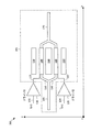
図1は、ZカットLiNbO3MZMドライバシステム100の実施形態の概略図であり、Zカットは、図1に図示されるように、MZMにおける結晶の偏光が表面に垂直なZ軸方向に配向されていることを意味する。ZカットMZMドライバシステム100は、ZカットMZM101と、近位ドライバ110および遠位ドライバ135を備える1対の相補的ドライバ(complementary driver)とを備える。したがって、ZカットMZM101は、時に、デュアル駆動MZMと称される。ZカットMZMドライバシステム100は、図示されるように、または任意の他の適切なやり方で構成されてよい。ZカットMZM101は、様々な材料で作られ得る。材料は、ニオブ酸リチウム(LiNbO3)などの強誘電性または電気光学的結晶を含み得る。ZカットMZM101は、入力光導波路105と、近位アーム導波路120と、遠位アーム導波路130と、近位アーム導波路120に結合された近位電極140と、遠位アーム導波路130に結合された遠位電極160と、アース150と、出力導波路170とを備える。
FIG. 1 is a schematic diagram of an embodiment of a Z-cut LiNbO 3
入力光導波路105は、光および/または変調された光信号を受信し、光信号の近位の半分/部分を近位アーム導波路120に、光信号の遠位の半分/部分を遠位アーム導波路130に、それぞれ伝達するように構成される。近位アーム導波路120は、近位電極140に電気的に結合され、遠位アーム導波路130は、遠位電極160に電気的に結合される。近位アーム導波路120および遠位アーム導波路130は、それぞれ、光信号の近位部分および光信号の遠位部分を、それぞれ電極140および160を越えて、変調のために、出力導波路170上へと伝達するように構成される。出力導波路170は、光信号の近位部分と光信号の遠位部分とを統合し、合成された光信号を、例えば、別の導波路、光ファイバに結合された導波路-ファイバ結合器などの外部コンポーネントへの出力のために伝達するように構成される。
The input
近位電極140は、近位ドライバ110に結合される。近位ドライバ110は、近位RF信号102を受信し、近位RF信号102を増幅して増幅された近位RF信号115を作り出し、増幅された近位RF信号115を近位電極140へと電気的に伝達するように構成される。近位電極140およびアース150は、近位アーム導波路120における自由電子を枯渇させることによって光信号の近位部分の位相を変調するように集合的に構成される。光信号の近位部分の位相変調は、増幅された近位RF信号115を近位アーム導波路120に印加して、自由電子を選択的に枯渇(例えば、枯渇モード)または近位アーム導波路120内に誘導(例えば、蓄積モード)し、それによって近位アーム導波路120の屈折率の変化を誘起することによって実施される。近位アーム導波路120の屈折率における変化は、近位アーム導波路120を伝播する光信号の速度を変え、結果として光信号の位相変調をもたらす。遠位ドライバ135は、遠位RF信号104を受信、増幅して増幅された遠位RF信号137を作り出し、増幅された遠位RF信号137を遠位電極160へと伝達し、実質的に同様のやり方で遠位アーム導波路130における光信号を変調する。それ故、近位アーム導波路120および遠位アーム導波路130における光信号の出力は、プッシュプル動作を使用して近位ドライバ110および遠位ドライバ135を独立して動作させることによって、光出力信号へと合成され得る。
光信号の近位部分および光信号の遠位部分の位相変調の振幅は、アース150に対する増幅された近位RF信号115および増幅された遠位RF信号137の電圧にそれぞれ明確に比例する。近位RF信号102と遠位RF信号104は、約180度の位相差を有する。結果として、光信号の近位部分および光信号の遠位部分の位相変調は、絶対値が同じだが符号が異なる。一実施形態において、近位RF信号102および遠位RF信号104は、2つの異なるRF発振器によって生成される。別の実施形態において、近位RF信号102および遠位RF信号104は、同一のRF発振器によって生成され、RFシフタによって、RF信号のうちの1つ(例えば遠位104)は、近位RF信号に対して180度の位相偏移を受ける。
The amplitude of the phase modulation of the proximal portion of the optical signal and the distal portion of the optical signal is clearly proportional to the voltages of the amplified
動作時には、光信号は入力光導波路105に導かれ、近位部分と遠位部分とに分割される。光信号の近位部分は、近位アーム導波路120内を進行し、近位位相変調を受ける。光信号の遠位部分は遠位アーム導波路130内に伝達され、遠位位相変調を受ける。近位位相変調および遠位位相変調の振幅は、絶対値が同じだが符号が異なる。次いで、外部コンポーネントとの通信のために、出力光導波路170において、光信号の近位部分は光信号の遠位部分と合成される。
In operation, the optical signal is directed to the input
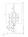
図2は、XカットLiNbO3MZMドライバシステム200の実施形態の概略図であり、Xカットは、図2に図示されるように、X軸方向が表面に垂直である一方、Z軸(結晶の偏光)は光導波路に垂直であることを意味する。XカットMZMドライバシステム200は、XカットMZM201とドライバ210とを備える。ドライバ210は、近位ドライバ110および遠位ドライバ135と同様である。XカットMZM201は、時に、単一駆動MZMと称される。XカットMZMドライバシステム200は、図示されるように、または任意の他の適切なやり方で構成されてよい。XカットMZM201は、ZカットMZM101と実質的に同様でよいが、異なる結晶偏光を有し、入力光導波路205と、近位アーム導波路220と、遠位アーム導波路230と、アース250と、出力導波路260とを備え、これらはそれぞれ、入力光導波路105、近位アーム導波路120、遠位アーム導波路130、アース150、および出力導波路170と同様である。
FIG. 2 is a schematic diagram of an embodiment of an X-cut LiNbO 3
XカットMZM201は電極240を備え、これは電極140および160と実質的に同様であるが、近位アーム導波路220と遠位アーム導波路230との間に配置される。電極240は、ドライバ210に電気的に結合される。ドライバ210は、RF信号204を受信し、信号を増幅して増幅されたRF信号215を作り出し、増幅されたRF信号215を、電極240を介して、近位アーム導波路220と遠位アーム導波路230との間に印加する。増幅されたRF信号215は、電極240とアース250との間で近位アーム導波路220および遠位アーム導波路230内において自由電子を枯渇させまたは誘起する。近位アーム導波路220および遠位アーム導波路230における結晶の偏光は、Z軸に沿って逆方向に構成され、結果として、増幅されたRF信号215が電極に印加されたときに同等かつ逆のふるまい(例えば、自由電子の枯渇または誘導)をもたらす。例えば、近位アーム導波路220および遠位アーム導波路230内を進行する光搬送波部分の位相シフトは、絶対値が同じだが符号が異なる。このように、近位アーム導波路220および遠位アーム導波路230の両方を横断する光搬送波は、単一のドライバ210によってプッシュプル手法で制御され得る。それ故、XカットMZM201は、同一の電圧および電気光学係数を与えられると、より少ないドライバで、ZカットMZM101と同一の量の位相変調を生成する。XカットMZMドライバシステム201の利点は、より単純な実装、全体的なドライバ-変調器システムのより小さな総サイズ、およびより低い電力消費を含む。
ZカットMZM101およびXカットMZM201のどちらにおいても、近位アーム導波路120および220ならびに遠位アーム導波路130および230の静電容量は比較的大きい。変調速度は静電容量に反比例するため、結果として、高速度(例えば、25Gbps変調速度よりも大きい)におけるZカットMZM101およびXカットMZM201の適用は限定される。加えて、MZM内を進行するRF信号の伝播速度は単位長さ当たりの静電容量の平方根に反比例するので、MZM内を進行するRF信号の伝播速度は、単位長さ当たりの静電容量が大きいため、光信号の伝播速度よりも大幅に遅くなる。
In both Z-cut MZM101 and X-cut MZM201, the capacitances of
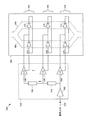
図3は、デュアル駆動マルチセグメントMZMドライバシステム300の実施形態の概略図である。デュアル駆動マルチセグメントMZMドライバシステム300は、駆動集積回路(IC)310と、マルチセグメント変調器360とを備える。デュアル駆動マルチセグメントMZMドライバシステム300は、図示されるように、または任意の他の適切なやり方で構成されてよい。デュアル駆動マルチセグメントMZMドライバシステム300は、複数の変調器セグメント370を用いており、そのそれぞれの総静電容量は、ZカットMZM101およびXカットMZM201の静電容量よりも実質的に小さい。変調器セグメント370は、マルチセグメント変調器360を横断する光信号の伝播遅延を考慮して近位RF信号320および遠位RF信号325にタイミング遅延を導入することによって同期される。このように、デュアル駆動マルチセグメントMZMドライバシステム300は、ZカットMZM101およびXカットMZM201よりも高速で変調され得る。
FIG. 3 is a schematic diagram of an embodiment of a dual drive multi-segment
駆動IC310は、各変調器セグメント370に対してセグメントドライバ350を備え、セグメントドライバ350は、送信ライン345を介して電気的に結合される。セグメントドライバ350はそれぞれ、対応する変調器セグメント370を近位ドライバ110および遠位ドライバ135と同様のプッシュプル手法で変調する近位出力352と遠位出力354と(例えば2つのドライバ)を備える。セグメントドライバ350はそれぞれ、送信ライン345および入力ドライバ340を介して受信された近位RF信号320および遠位RF信号325を用いて近位出力352および遠位出力354を生成する。近位RF信号320および遠位RF信号325は、それぞれ、近位RF信号102および遠位RF信号104と同様である。駆動IC310は、入力ドライバ340を用いて、送信ライン345を介した送信のために必要に応じて近位RF信号320および遠位RF信号325を増幅する。近位RF信号320および遠位RF信号325を供給するデバイスの電気的特性が駆動IC310の電気的特性を変えてしまうことを防止するためのインピーダンス整合を行うために、入力ドライバ340は、アースされた抵抗330および335(例えば、50オーム(Ω)抵抗)とともに動作し得る。送信ラインは抵抗342を介して結合されて、送信ライン345の回路を完成させる。駆動IC310は、動作電力を受け取るために電源(例えば、5.2ボルト(V)電源)およびアースに結合される。駆動IC310は、図示される例においては、直流(DC)コントロール312および314によって制御される。11個のセグメントドライバ350が図示されているが、変調器セグメント370の数に応じて任意の数のセグメントドライバ350が用いられてよいことに留意されたい。
The
マルチセグメント変調器360は、近位アーム導波路380と、遠位アーム導波路390とを備え、これらはそれぞれ、近位アーム導波路120および220ならびに遠位アーム導波路130および230と同様である。近位アーム導波路380および遠位アーム導波路390は、変調器セグメント370およびバイアスセグメント365を介して光搬送波を伝播する。各変調器セグメント370は、近位アーム導波路380および遠位アーム導波路390のそれぞれにまたはそれらに隣接して配置される一対のキャパシタ376を備える。近位アーム導波路380の各キャパシタ376(例えば、近位キャパシタ)は、対応するセグメントドライバ350の近位出力352に電気的に結合され、遠位アーム導波路390の各キャパシタ376(例えば、遠位キャパシタ)は、対応するセグメントドライバ350の遠位出力354に電気的に結合される。それ故、各キャパシタ376は、対応する導波路アーム380/390において電子を枯渇または増大させて、セグメントドライバ350の出力に基づいてZカットMZM101と同様のやり方によりプッシュプル手法で光信号の部分/ステージを変調することができる。変調器セグメント370は、キャパシタ376に送られる近位出力352および遠位出力354を調整するためのインダクタ372および抵抗374を更に備える。各キャパシタ376は、導波路アーム全体にわたって枯渇/増大を管理するために、電圧源(または、実施形態によってはアース)にも結合される。バイアスセグメント365は、光信号の任意の必要とされる補正調整を提供する。バイアスセグメント365は、マッハツェンダー干渉計(MZI)バイアスコントロール362および364に基づいて光信号を変調するためのキャパシタ368と、必要に応じてMZIバイアス信号を調整するための抵抗366とを備える。MZIバイアスコントロール362および364は、変調器セグメント370と実質的に同様のやり方で光信号を変調するが、変調された信号を、出力のために信号が統合される前に、微細にチューニングするために用いられる。
動作時には、近位RF信号320および遠位RF信号325は、時間調整されつつ各セグメントドライバ350に伝播され、次いで光搬送波における変調のために各変調器セグメント370に転送される。光搬送波が導波路アーム380および390に沿って伝播するのに伴って、光搬送波は、各変調器セグメント370において変調される。近位RF信号320および遠位RF信号325は、光搬送波の速度に整合するように信号が適切な変調器セグメント370に適切な時点において到達するように時間調整され、最終的な統合および出力のためにバイアスセグメント365において完全な変調された光信号が受信されるようにする。マルチセグメント変調器360は、ZカットMZM101およびXカットMZM201と比べると、セグメント当たりの静電容量を減少させるが、各変調器セグメント370に対してデュアルセグメントドライバ350を必要とする。
In operation, the
図4は、単一駆動マルチセグメントMZMドライバシステム400の実施形態の概略図である。単一駆動マルチセグメントMZMドライバシステム400は、デュアル駆動マルチセグメントMZMドライバシステム300と同様に動作するが、各変調器セグメント470に対してセグメントドライバ440を用いている。単一駆動マルチセグメントMZMドライバシステム400は、高速動作(例えば、25ギガヘルツ(GHz)よりも大きい)のために用いられ得るが、必要とされる電力、複雑さはシステム300よりも小さい。単一駆動マルチセグメントMZMドライバシステム400は、図示されるように、または任意の他の適切なやり方で構成され、駆動IC410と、マルチセグメント変調器460とを備える。
FIG. 4 is a schematic diagram of an embodiment of a single drive multi-segment
駆動IC410は、入力ドライバ430と、セグメントドライバ440と、RF入力信号420を伝播するための送信ライン450とを備え、これらはそれぞれ、入力ドライバ340、セグメントドライバ350、および送信ライン345と同様である。駆動IC410は、駆動IC310とは異なり、駆動IC410は、マルチセグメント変調器460の各変調器セグメント470に対して単一のRF入力信号420および単一のセグメントドライバ440を含む。駆動IC410は、必要に応じて、インピーダンス整合のための抵抗/インダクタと、DCコントロールおよび/または電源も備えてよい。11個のセグメントドライバ440が図示されているが、変調器セグメント470の数に応じて任意の数のセグメントドライバ440が用いられてよい。セグメントドライバ440は、相補型金属酸化膜半導体(CMOS)インバータとして実装されてよく、これは比較的電力消費が小さい。各セグメントドライバ440は、単一の入力を受信し、単一の出力を伝達する。光信号との速度整合のためのセグメントドライバ440間の時間遅延は、RF入力信号420によって送信ライン450に提供される。遅延は、1つまたは複数のCMOS回路によって能動的に生成されることも可能である。時間経過とともにセグメントドライバ440を選択的に無効にする(例えば、低または高に設定された出力)ことによって、ドライバ440の出力が2つの電気レベルしか有さない場合でも、パルス振幅変調(PAM)などのマルチレベルの光信号が生成され得る。
The
マルチセグメント変調器460は、シリコン、リン化インジウム(InP)、および/またはガリウムヒ素(GaAs)から作られ得る。マルチセグメント変調器460は、近位アーム導波路480と遠位アーム導波路490とを備え、これらはそれぞれ、近位アーム導波路380および遠位アーム導波路390と同様であり、セグメントドライバ440に対応する複数の変調器セグメント470によって変調される。各変調器セグメント470は、近位ダイオード476と遠位ダイオード475とを備え、これらはそれぞれ、近位アーム導波路480および遠位アーム導波路490上に/それらに隣接して配置される。ダイオード475および476は、正-負(p-n)ダイオードとも称され得、電圧制御された可変キャパシタとして働き得る。ダイオード475および476は、XカットMZM201と同一の極性で配向されてよい。ダイオード475および476はそれぞれ、負電荷を帯びたカソードと正電荷を帯びたアノードとを備える。各セグメントドライバ440は、図4に図示されるように、近位ダイオード476のカソードおよび遠位ダイオード475のアノードに結合され得る。代替的には、各セグメントドライバ440は、近位ダイオード476のアノードおよび遠位ダイオード475のカソードに結合され得る。どちらの場合においても、セグメントドライバ440は、セグメント対における各ダイオードがセグメントドライバ440に対して逆の極性を有するように、一方のダイオードの負の部分および他方のダイオードの正の部分に結合される。セグメントドライバ440に結合されない各ダイオードのインターフェースは、交流(AC)信号をサポートするためにアースに結合され得る。ダイオードが所望のDC電圧でバイアスがかけられるように、DC絶縁が用いられてよい。例えば、DC絶縁は、大容量のキャパシタを各ダイオード475および476とそれぞれのアースとの間に挿入することによって実施され得る。各アームにおけるダイオードの極性は信号接続点に関して互いに逆向きに配されているので、駆動信号は結果として、導波路の各アームにおいて逆に位相シフトするが、値は等しくなる。このように、単一のセグメントドライバ440は、一対のセグメントドライバ350と同一の量の枯渇/蓄積(および、それ故に変調)を各導波路アームにおいて生成する。それ故、セグメントドライバ440を一対の逆に帯電されたダイオード475および476に結合することによって、デュアル駆動マルチセグメントMZMドライバシステム300と比べると、同一の変調パワー、光信号振幅、変調速度などを維持しながら、送信ライン450およびセグメントドライバ440の数は半分に減少され得る。
図5は、単一駆動マルチセグメントMZMドライバシステム500の別の実施形態の概略図である。単一駆動マルチセグメントMZMドライバシステム500は、単一駆動マルチセグメントMZMドライバシステム400と実質的に同様であるが、駆動IC510の各セグメントドライバ540は、入力バッファ530および送信ライン550を介して受信される単一のRF入力信号520に基づく主出力(primary output)および相補的出力(complementary output)の両方を用いている。主出力は、相補的出力と同一であるが、逆の電荷/符号を備える。例えば、主出力が約+0.5ボルトであれば、相補的出力は同時に約-0.5ボルトである。駆動IC510、RF入力信号520、入力バッファ530、送信ライン550、およびセグメントドライバ540は、他の点においては、それぞれ、駆動IC410、RF入力信号420、入力ドライバ430、送信ライン450、およびセグメントドライバ440と実質的に同様であってよい。単一駆動マルチセグメントMZMドライバシステム500は、近位アーム導波路580と、遠位アーム導波路590と、遠位ダイオード575および近位ダイオード576を備える変調器セグメント570とを備えるマルチセグメント変調器560を更に備え得、これらはそれぞれ、近位アーム導波路480、遠位アーム導波路490、遠位ダイオード475、近位ダイオード476、変調器セグメント470、およびマルチセグメント変調器460と同様であってよい。各セグメントドライバ540の主出力は、近位ダイオード576のカソードおよび遠位ダイオード575のアノードに結合される一方、相補的出力は近位ダイオード576のアノードおよび遠位ダイオード575のカソードに結合されるか、またはその逆である(例えば、主出力は相補的出力とは異なるインターフェースに結合される)。変調器セグメント470からのアース接続を相補的出力で置き換えることによって、各変調器セグメント570の有効駆動電圧は、セグメントドライバ540または送信ライン550の数を増やすことなく2倍になる。図4のものと同様に、ダイオードに所望のDC電圧でバイアスがかけられるように、DC絶縁が用いられてよい。各変調器セグメント570への出力の電圧を2倍にすることにより、より大きな微分位相シフト、したがってより高い変調度が達成され得、結果としてより大きな変調効率をもたらす。更に、MZMの長さが短縮され得、結果としてより大きな変調効率をもたらす。
FIG. 5 is a schematic diagram of another embodiment of a single drive multi-segment
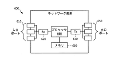
図6は、ネットワーク要素(NE)600の実施形態の概略図である。NE600は、データを受信するための入口ポート(ingress port)610および受信機ユニット(Rx)620と、データを処理するためのプロセッサ、論理ユニットまたは中央処理ユニット(CPU)630と、光信号上のデータを変調し、光信号を送信するための光送信機ユニット(Tx)640および出口ポート(egress port)650と、データを記憶するためのメモリ660とを含む。Tx640は、単一駆動マルチセグメントMZMドライバシステム400および/または500を備え得る。ネットワーク要素600は、図示されるように、または任意の他の適切なやり方で構成されてよい。
FIG. 6 is a schematic diagram of an embodiment of a network element (NE) 600. The
プロセッサ630は、データを処理するように構成され、入口ポート610、受信機ユニット620、送信機ユニット640、出口ポート650、およびメモリ660と通信している。メモリ660は、1つまたは複数のディスク、テープドライブ、およびソリッドステートドライブを含み、プログラムが実行のために選択されたときにそのプログラムを記憶し、プログラム実行中に読み出される命令およびデータを記憶するために、オーバーフローデータ記憶デバイスとして使用され得る。メモリ660は、揮発性および不揮発性でよく、読み出し専用メモリ(ROM)、ランダムアクセスメモリ(RAM)、3値連想メモリ(TCAM:ternary content-addressable memory)、およびスタティックランダムアクセスメモリ(SRAM)であってよい。
The
いくつかの実施形態において、NE600は、近位RF信号102および遠位RF信号104を生成するようにプログラムされる。いくつかの実施形態において、NE600は、RF信号204を生成するようにプログラムされる。いくつかの実施形態において、NE600は、近位RF信号320、遠位RF信号325、MZIバイアスコントロール362および364、ならびにDCコントロール312および314を生成するようにプログラムされる。いくつかの実施形態において、NE600は、RF信号420を生成するようにプログラムされる。いくつかの実施形態において、NE600は、RF信号520を生成するようにプログラムされる。
In some embodiments,
実行可能な命令をNE600にプログラムおよび/またはロードすることにより、プロセッサ630および/またはメモリデバイス660のうちの少なくとも1つが変更され、NE600を、本開示によって教示される新規な機能性を有する、特定の機械または装置、例えば、マルチコア転送アーキテクチャへと部分的に転換することが理解されよう。実行可能なソフトウェアをコンピュータにロードすることによって実装可能な機能性が、既知の設計規則によってハードウェア実装へと変換され得ることは、電気技術およびソフトウェア技術の分野の基本である。概念をソフトウェアとして実装するかハードウェアとして実装するかの判断は、ソフトウェア領域からハードウェア領域に変換する際に関係する何らかの問題点ではなく、典型的には、設計の安定性および生み出されるユニットの数を考慮して決まる。概して、ハードウェア実装の再設計(re-spinning)は、ソフトウェア設計を再設計するよりも高価であるので、いまなお頻繁な変更がなされる設計は、ソフトウェアとして実装されることが好ましくなり得る。概して、大量生産が行われるとハードウェア実装はソフトウェア実装よりも安価となり得るので、安定的で大量に製造される設計は、ハードウェア、例えば、ASICとして実装されることが好ましくなり得る。多くの場合、設計は、ソフトウェア形態で開発、テストされ、その後、既知の設計規則によって、ソフトウェアの命令を有線接続化したASICにおける同等のハードウェア実装へと転換され得る。新たなASICによってコントロールされる機械が特定の機械または装置であるのと同じように、実行可能な命令がプログラムおよび/またはロードされたコンピュータは、特定の機械または装置と見なされてよい。
By programming and / or loading executable instructions into the
本開示においていくつかの実施形態が提供されたが、開示されたシステムおよび方法は、本開示の趣旨または範囲から逸脱することなく、多くの他の特定の形態で具現化され得ることを理解されたい。本例は、制限的なものではなく、例示的なものと見なされるべきであり、その意図は本明細書によって与えられる詳細に限定されない。例えば、様々な要素またはコンポーネントは、組み合わせられてよく、もしくは別のシステムに一体化されてよく、またはある特徴は、省略されてよく、もしくは実装されなくてよい。 While several embodiments have been provided in this disclosure, it is understood that the disclosed systems and methods may be embodied in many other specific forms without departing from the spirit or scope of this disclosure. I want. This example should not be construed as limiting, but rather exemplary and the intent is not limited to the details provided herein. For example, various elements or components may be combined or integrated into another system, or certain features may be omitted or not implemented.
加えて、様々な実施形態において、別個のものまたは分離したものとして説明され、示された技術、システム、サブシステム、および方法は、本開示の範囲から逸脱することなく、他のシステム、モジュール、技術、または方法との組合せまたは一体化がなされ得る。互いに結合される、互いに直接的に結合されるまたは互いに通信するものとして図示または説明された他のアイテムは、電気的、機械的、またはその他の態様であるか否かかかわらず、いくつかのインターフェース、デバイス、または中間コンポーネントを介して、間接的に結合されまたは通信してよい。変更、代用、および改変の他の例は、当業者によって認識可能であり、本明細書で開示された趣旨および範囲から逸脱することなくなされ得る。 In addition, in various embodiments, the techniques, systems, subsystems, and methods described and illustrated as separate or separate may be used for other systems, modules, modules, and the like without departing from the scope of this disclosure. Combinations or integrations with technologies or methods may be made. Other items illustrated or described as being coupled to each other, directly coupled to each other, or in communication with each other include several interfaces, whether electrical, mechanical, or otherwise. , Devices, or intermediate components, which may be indirectly coupled or communicated. Other examples of changes, substitutions, and modifications will be recognized by those skilled in the art and may be made without departing from the spirit and scope disclosed herein.
100 ZカットLiNbO3MZMドライバシステム
101 ZカットMZM
102 近位RF信号
104 遠位RF信号
105 入力光導波路
110 近位ドライバ
115 増幅された近位RF信号
120 近位アーム導波路
130 遠位アーム導波路
135 遠位ドライバ
137 増幅された遠位RF信号
140 近位電極
150 アース
160 遠位電極
170 出力導波路
200 XカットLiNbO3MZMドライバシステム
201 XカットMZM
204 RF信号
205 入力光導波路
210 ドライバ
215 増幅されたRF信号
220 近位アーム導波路
230 遠位アーム導波路
240 電極
250 アース
260 出力導波路
300 デュアル駆動マルチセグメントMZMドライバシステム
310 駆動集積回路(IC)、駆動IC
312 直流(DC)コントロール
314 直流(DC)コントロール
320 近位RF信号
325 遠位RF信号
330 抵抗
335 抵抗
340 入力ドライバ
342 抵抗
345 送信ライン
350 セグメントドライバ
352 近位出力
354 遠位出力
360 マルチセグメント変調器
362 マッハツェンダー干渉計(MZI)バイアスコントロール
364 マッハツェンダー干渉計(MZI)バイアスコントロール
365 バイアスセグメント
366 抵抗
368 キャパシタ
370 変調器セグメント
372 インダクタ
374 抵抗
376 キャパシタ
380 近位アーム導波路
390 遠位アーム導波路
400 単一駆動マルチセグメントMZMドライバシステム
410 駆動IC
420 RF入力信号
430 入力ドライバ
440 セグメントドライバ
450 送信ライン
460 マルチセグメント変調器
470 変調器セグメント
475 遠位ダイオード
476 近位ダイオード
480 近位アーム導波路
490 遠位アーム導波路
500 単一駆動マルチセグメントMZMドライバシステム
510 駆動IC
520 RF入力信号
530 入力バッファ
540 セグメントドライバ
550 送信ライン
560 マルチセグメント変調器
570 変調器セグメント
575 遠位ダイオード
576 近位ダイオード
580 近位アーム導波路
590 遠位アーム導波路
600 ネットワーク要素(NE)
610 入口ポート
620 受信機ユニット(Rx)
630 プロセッサ、論理ユニット、中央処理ユニット(CPU)
640 光送信機ユニット(Tx)
650 出口ポート
660 メモリ、メモリデバイス
100 Z cut LiNbO 3 MZM driver system
101 Z cut MZM
102 Proximal RF signal
104 Distant RF signal
105 Input optical waveguide
110 Proximal driver
115 Amplified proximal RF signal
120 Proximal arm waveguide
130 Distal arm waveguide
135 Distal driver
137 Amplified distal RF signal
140 Proximal electrode
150 Earth
160 Distal electrode
170 Output waveguide
200 X-cut LiNbO 3 MZM driver system
201 X cut MZM
204 RF signal
205 Input optical waveguide
210 drivers
215 Amplified RF signal
220 Proximal arm waveguide
230 Distal arm waveguide
240 electrodes
250 Earth
260 Output waveguide
300 Dual drive multi-segment MZM driver system
310 Drive integrated circuit (IC), drive IC
312 DC control
314 Direct Current (DC) Control
320 Proximal RF signal
325 Distant RF signal
330 resistance
335 resistance
340 input driver
342 resistance
345 transmission line
350 segment driver
352 Proximal output
354 Distal output
360 multi-segment modulator
362 Mach-Zehnder Interferometer (MZI) Bias Control
364 Mach-Zehnder Interferometer (MZI) Bias Control
365 bias segment
366 resistance
368 capacitors
370 modulator segment
372 inductor
374 resistance
376 capacitors
380 Proximal arm waveguide
390 Distal arm waveguide
400 single drive multi-segment MZM driver system
410 Drive IC
420 RF input signal
430 input driver
440 segment driver
450 transmission line
460 Multi-segment modulator
470 modulator segment
475 Distant diode
476 Proximal diode
480 proximal arm waveguide
490 Distal arm waveguide
500 single drive multi-segment MZM driver system
510 Drive IC
520 RF input signal
530 input buffer
540 segment driver
550 transmission line
560 multi-segment modulator
570 modulator segment
575 Distal diode
576 proximal diode
580 Proximal arm waveguide
590 Distal arm waveguide
600 Network Element (NE)
610 Inlet port
620 Receiver unit (Rx)
630 Processor, logical unit, central processing unit (CPU)
640 Optical transmitter unit (Tx)
650 exit port
660 memory, memory device
Claims (20)
光信号を伝播するための導波路であって、
前記光信号の近位部分を伝達するように構成された近位アーム、および
前記光信号の遠位部分を伝達するように構成された遠位アーム
を備える導波路と、
前記光信号の前記近位部分を変調するように構成された近位ダイオードと、
前記光信号の前記遠位部分を変調するように構成された遠位ダイオードと、
前記近位ダイオードおよび前記遠位ダイオードの逆符号のインターフェースに電気的に結合された電気的入力であって、前記電気的入力に沿って伝播される電気駆動信号が、前記導波路の前記近位アームにおける前記光信号の前記近位部分と前記導波路の前記遠位アームにおける前記光信号の前記遠位部分との同等かつ逆の変調を起こす、電気的入力と
を備える、光変調器。 An optical modulator,
A waveguide for propagating an optical signal,
A waveguide comprising a proximal arm configured to transmit a proximal portion of the optical signal, and a distal arm configured to transmit a distal portion of the optical signal;
A proximal diode configured to modulate the proximal portion of the optical signal;
A distal diode configured to modulate the distal portion of the optical signal;
An electrical input electrically coupled to an opposite sign interface of the proximal diode and the distal diode, wherein an electrical drive signal propagated along the electrical input is transmitted to the proximal of the waveguide An optical modulator comprising: an electrical input that causes equal and opposite modulation of the proximal portion of the optical signal in the arm and the distal portion of the optical signal in the distal arm of the waveguide.
光変調器であって、
複数の電気的セグメント入力、
光信号の近位の半分を伝達するように構成された近位導波路アーム、
前記光信号の遠位の半分を伝達するように構成された遠位導波路アーム、および
複数の変調器セグメントであって、各変調器セグメントは、対応する電気的セグメント入力を前記近位導波路アームおよび前記遠位導波路アームの両方の上に変調するように構成される、複数の変調器セグメント
を備える光変調器と、
前記光変調器に電気的に結合され、前記複数の変調器セグメントに対応する複数のドライバを備え、各ドライバは、単一の対応する変調器セグメントによって変調を制御するために、単一の対応する電気的セグメント入力に対して電気的セグメント信号を出力する、駆動回路と
を備える、単一駆動マルチセグメント光変調器システム。 A single drive multi-segment optical modulator system comprising:
An optical modulator,
Multiple electrical segment inputs,
A proximal waveguide arm configured to transmit the proximal half of the optical signal;
A distal waveguide arm configured to transmit a distal half of the optical signal, and a plurality of modulator segments, each modulator segment receiving a corresponding electrical segment input to the proximal waveguide An optical modulator comprising a plurality of modulator segments configured to modulate on both the arm and the distal waveguide arm;
A plurality of drivers electrically coupled to the light modulator and corresponding to the plurality of modulator segments, each driver having a single counterpart to control modulation by a single corresponding modulator segment And a drive circuit for outputting an electrical segment signal to the electrical segment input.
Applications Claiming Priority (5)
| Application Number | Priority Date | Filing Date | Title |
|---|---|---|---|
| US201462041544P | 2014-08-25 | 2014-08-25 | |
| US62/041,544 | 2014-08-25 | ||
| US14/832,909 | 2015-08-21 | ||
| US14/832,909 US9733542B2 (en) | 2014-08-25 | 2015-08-21 | Multi-segment Mach-Zehnder modulator-driver system |
| PCT/CN2015/087987 WO2016029836A1 (en) | 2014-08-25 | 2015-08-25 | Multi-segment mach-zehnder modulator-driver system |
Publications (2)
| Publication Number | Publication Date |
|---|---|
| JP2017531202A true JP2017531202A (en) | 2017-10-19 |
| JP6493895B2 JP6493895B2 (en) | 2019-04-03 |
Family
ID=55398759
Family Applications (1)
| Application Number | Title | Priority Date | Filing Date |
|---|---|---|---|
| JP2017511276A Active JP6493895B2 (en) | 2014-08-25 | 2015-08-25 | Multi-segment Mach-Zehnder modulator driver system |
Country Status (6)
| Country | Link |
|---|---|
| US (1) | US9733542B2 (en) |
| EP (1) | EP3177961B1 (en) |
| JP (1) | JP6493895B2 (en) |
| CN (1) | CN106575050B (en) |
| BR (1) | BR112017003863B1 (en) |
| WO (1) | WO2016029836A1 (en) |
Families Citing this family (25)
| Publication number | Priority date | Publication date | Assignee | Title |
|---|---|---|---|---|
| US10928659B2 (en) | 2014-02-24 | 2021-02-23 | Rockley Photonics Limited | Optoelectronic device |
| JP6330549B2 (en) * | 2014-07-25 | 2018-05-30 | 住友電気工業株式会社 | Optical semiconductor device and manufacturing method thereof |
| US10921616B2 (en) | 2016-11-23 | 2021-02-16 | Rockley Photonics Limited | Optoelectronic device |
| US11150494B2 (en) | 2015-03-05 | 2021-10-19 | Rockley Photonics Limited | Waveguide modulator structures |
| US20170285436A1 (en) * | 2015-11-04 | 2017-10-05 | Coriant Advanced Technology, LLC | Differential phase biasing modulator apparatus and method |
| US10914968B2 (en) * | 2016-03-24 | 2021-02-09 | Huawei Technologies Canada Co., Ltd. | Photonic elements driven by common electrical driver |
| US10120210B2 (en) | 2016-06-03 | 2018-11-06 | International Business Machines Corporation | Feed-forward optical equalization using an electro-optic modulator with a multi-segment electrode and distributed drivers |
| US10084619B2 (en) | 2016-06-03 | 2018-09-25 | International Business Machines Corporation | Nested feed-forward optical equalization using an electro-optic modulator with a multi-segment electrode |
| US11101256B2 (en) * | 2016-11-23 | 2021-08-24 | Rockley Photonics Limited | Optical modulators |
| GB2559458B (en) | 2016-12-02 | 2020-06-03 | Rockley Photonics Ltd | Waveguide device and method of doping a waveguide device |
| US11105975B2 (en) | 2016-12-02 | 2021-08-31 | Rockley Photonics Limited | Waveguide optoelectronic device |
| US10353267B2 (en) * | 2016-12-30 | 2019-07-16 | Huawei Technologies Co., Ltd. | Carrier-effect based optical switch |
| JP6900764B2 (en) * | 2017-04-27 | 2021-07-07 | 富士通株式会社 | Optical transmitter |
| FR3067532B1 (en) * | 2017-06-12 | 2019-06-21 | Commissariat A L'energie Atomique Et Aux Energies Alternatives | M-PAM MODULATION TRANSMITTER FOR WIRELESS OPTICAL COMMUNICATION SYSTEM |
| JP6998691B2 (en) * | 2017-07-19 | 2022-01-18 | 日本ルメンタム株式会社 | Optical transmission module |
| JP7139965B2 (en) * | 2019-01-16 | 2022-09-21 | 日本電信電話株式会社 | Semiconductor Mach-Zehnder optical modulator |
| US20230078976A1 (en) * | 2020-02-21 | 2023-03-16 | Universiteit Gent | Mach-zehnder modulator |
| JP7600725B2 (en) * | 2021-01-28 | 2024-12-17 | 住友電気工業株式会社 | Manufacturing method, test method, and test program for optical modulator, and optical transmitter |
| US11630335B2 (en) * | 2021-02-08 | 2023-04-18 | Globalfoundries U.S. Inc. | Optical power modulators with unloaded transmission lines |
| WO2022225559A1 (en) * | 2021-04-22 | 2022-10-27 | Futurewei Technologies, Inc. | Tapered impedance traveling wave mach-zehnder modulator |
| JP7749907B2 (en) * | 2021-07-16 | 2025-10-07 | ホアウェイ・テクノロジーズ・カンパニー・リミテッド | Electro-optic modulator, optical modulation system, and integrated optical chip |
| US12019350B2 (en) * | 2021-12-23 | 2024-06-25 | Nokia Solutions And Networks Oy | Multi-segment electro-optic devices with low loss RF delay lines |
| WO2023132888A1 (en) * | 2022-01-07 | 2023-07-13 | Rensselaer Polytechnic Institute | Slow-light photonic modulators for radio-frequency photonic systems |
| US12174468B2 (en) * | 2022-01-14 | 2024-12-24 | Huawei Technologies Co., Ltd. | Method, apparatus and system for limited-range impedance tuning for silicon photonics devices |
| CN117311017A (en) * | 2022-06-22 | 2023-12-29 | 华为技术有限公司 | Light modulation systems and light modulators |
Citations (5)
| Publication number | Priority date | Publication date | Assignee | Title |
|---|---|---|---|---|
| JPH10333106A (en) * | 1997-05-28 | 1998-12-18 | Nec Corp | Semiconductor Mach-Zehnder modulator and manufacturing method thereof |
| US20020071622A1 (en) * | 2000-09-15 | 2002-06-13 | Massachusetts Institute Of Technology | Optical modulator using simultaneous push-pull drive of linear and quadratic electro-optic effects |
| JP2004318094A (en) * | 2003-04-10 | 2004-11-11 | Northrop Grumman Corp | Single electrode push-pull structure for semiconductor pin modulator |
| WO2011043079A1 (en) * | 2009-10-09 | 2011-04-14 | 日本電気株式会社 | Optical modulator module and method for modulating optical signal |
| JP2012529674A (en) * | 2009-06-12 | 2012-11-22 | ライトワイヤー,インク. | Silicon-type light modulator with improved efficiency and chirp control |
Family Cites Families (17)
| Publication number | Priority date | Publication date | Assignee | Title |
|---|---|---|---|---|
| US6650458B1 (en) * | 2002-09-26 | 2003-11-18 | Bookham Technology Plc | Electro-optic modulator with continuously adjustable chirp |
| EP1424591A1 (en) | 2002-11-22 | 2004-06-02 | Corning O.T.I. SRL | Electro-optical modulator and method of modulating optical signals |
| WO2004068221A1 (en) * | 2003-01-30 | 2004-08-12 | Fujitsu Limited | Optical modulator |
| US7212326B2 (en) * | 2003-05-30 | 2007-05-01 | Jds Uniphase Corporation | Optical external modulator |
| US7978390B2 (en) * | 2006-08-30 | 2011-07-12 | Hitachi, Ltd. | Optical modulator |
| WO2008048434A2 (en) * | 2006-10-07 | 2008-04-24 | Sioptical, Inc. | Segmented optical modulator |
| US7483597B2 (en) * | 2006-10-19 | 2009-01-27 | Lightwire, Inc. | Optical modulator utilizing multi-level signaling |
| US8731410B2 (en) | 2007-10-02 | 2014-05-20 | Luxtera, Inc. | Method and system for split voltage domain receiver circuits |
| US8238014B2 (en) * | 2008-09-08 | 2012-08-07 | Luxtera Inc. | Method and circuit for encoding multi-level pulse amplitude modulated signals using integrated optoelectronic devices |
| US8879873B2 (en) * | 2011-02-25 | 2014-11-04 | Nippon Telegraph And Telephone Corporation | Optical modulator |
| WO2012157182A1 (en) * | 2011-05-13 | 2012-11-22 | 日本電気株式会社 | Synchronous signal transmission system, synchronous drive system for optical modulator, synchronous signal transmission method, and non-temporary computer-readable medium storing program therefor |
| EP2615490B1 (en) | 2012-01-12 | 2016-11-30 | Fraunhofer-Gesellschaft zur Förderung der angewandten Forschung e.V. | Mach-zehnder modulator arrangement and method for operating a mach-zehnder modulator arrangement |
| US9459511B2 (en) * | 2012-04-27 | 2016-10-04 | Nec Corporation | Mach-Zehnder type optical modulator, optical transmission/reception system and control method of Mach-Zehnder type optical modulator |
| US9229250B2 (en) | 2012-10-11 | 2016-01-05 | Stmicroelectronics S.R.L. | Electro-optical modulator interface |
| EP2915002A1 (en) | 2012-10-31 | 2015-09-09 | Commissariat à l'Énergie Atomique et aux Énergies Alternatives | Device for generating a modulation of an optical signal comprising electro-absorption modulators |
| JP2014122964A (en) | 2012-12-20 | 2014-07-03 | Nec Corp | Optical modulator, optical transmitter, optical transmission/reception system, and control method of optical modulator |
| JP6220160B2 (en) * | 2013-05-31 | 2017-10-25 | キヤノン株式会社 | Reproducing apparatus and control method thereof |
-
2015
- 2015-08-21 US US14/832,909 patent/US9733542B2/en active Active
- 2015-08-25 WO PCT/CN2015/087987 patent/WO2016029836A1/en not_active Ceased
- 2015-08-25 EP EP15836087.5A patent/EP3177961B1/en active Active
- 2015-08-25 JP JP2017511276A patent/JP6493895B2/en active Active
- 2015-08-25 CN CN201580044947.5A patent/CN106575050B/en active Active
- 2015-08-25 BR BR112017003863-3A patent/BR112017003863B1/en active IP Right Grant
Patent Citations (5)
| Publication number | Priority date | Publication date | Assignee | Title |
|---|---|---|---|---|
| JPH10333106A (en) * | 1997-05-28 | 1998-12-18 | Nec Corp | Semiconductor Mach-Zehnder modulator and manufacturing method thereof |
| US20020071622A1 (en) * | 2000-09-15 | 2002-06-13 | Massachusetts Institute Of Technology | Optical modulator using simultaneous push-pull drive of linear and quadratic electro-optic effects |
| JP2004318094A (en) * | 2003-04-10 | 2004-11-11 | Northrop Grumman Corp | Single electrode push-pull structure for semiconductor pin modulator |
| JP2012529674A (en) * | 2009-06-12 | 2012-11-22 | ライトワイヤー,インク. | Silicon-type light modulator with improved efficiency and chirp control |
| WO2011043079A1 (en) * | 2009-10-09 | 2011-04-14 | 日本電気株式会社 | Optical modulator module and method for modulating optical signal |
Also Published As
| Publication number | Publication date |
|---|---|
| CN106575050B (en) | 2019-10-22 |
| WO2016029836A1 (en) | 2016-03-03 |
| JP6493895B2 (en) | 2019-04-03 |
| EP3177961A4 (en) | 2017-07-12 |
| EP3177961B1 (en) | 2019-05-29 |
| CN106575050A (en) | 2017-04-19 |
| BR112017003863B1 (en) | 2022-05-24 |
| US20160062207A1 (en) | 2016-03-03 |
| EP3177961A1 (en) | 2017-06-14 |
| US9733542B2 (en) | 2017-08-15 |
| BR112017003863A2 (en) | 2018-06-26 |
Similar Documents
| Publication | Publication Date | Title |
|---|---|---|
| JP6493895B2 (en) | Multi-segment Mach-Zehnder modulator driver system | |
| GB2546279B (en) | An optical apparatus | |
| US9454059B1 (en) | MZM linear driver for silicon photonics | |
| US5515196A (en) | Optical intensity and phase modulators in an optical transmitter apparatus | |
| US10120210B2 (en) | Feed-forward optical equalization using an electro-optic modulator with a multi-segment electrode and distributed drivers | |
| CN104216196B (en) | Tunable all-optical microwave photon frequency conversion device without external electric local oscillator | |
| US9784995B2 (en) | Multi-segment ring modulator | |
| US20130094797A1 (en) | Optical Transmitter With Tunable Chirp | |
| CN101232330A (en) | Control method of optical phase modulator | |
| JP6701115B2 (en) | Optical transmitter | |
| US6552838B2 (en) | LiNbO3 Mach-Zehnder modulator with low drive voltage requirement and adjustable chirp | |
| CN103135262A (en) | Electro-optical single-sideband modulator | |
| JP4184131B2 (en) | Optical SSB modulator | |
| JPH02269309A (en) | Optical modulating system | |
| Fallahpour et al. | Experimental generation of a 64-QAM by optically aggregating three independent QPSK channels using nonlinear wave mixing of multiple Kerr comb lines | |
| JP3249884B2 (en) | Apparatus and method for modulating polarized light signal | |
| JP2658387B2 (en) | Optical modulator, driving method thereof, and optical modulator driving device | |
| CN113824499B (en) | Overhead OPGW optical transmission method and system based on dual-drive MZM | |
| JP2823872B2 (en) | Optical transmitter | |
| US9915849B2 (en) | Optical modulator | |
| CN209657053U (en) | A kind of negative chirped modulation device of low pressure | |
| US20150331262A1 (en) | Optical modulator, optical transmitter, optical transmission/reception system, and control method for optical modulator | |
| JP2016151594A (en) | Optical modulator | |
| CN205452778U (en) | Linear frequency modulation narrow linewidth fiber laser in broadband | |
| CN104734783B (en) | A kind of random waveform optical pulse generator |
Legal Events
| Date | Code | Title | Description |
|---|---|---|---|
| A521 | Request for written amendment filed |
Free format text: JAPANESE INTERMEDIATE CODE: A523 Effective date: 20170406 |
|
| A621 | Written request for application examination |
Free format text: JAPANESE INTERMEDIATE CODE: A621 Effective date: 20170406 |
|
| A977 | Report on retrieval |
Free format text: JAPANESE INTERMEDIATE CODE: A971007 Effective date: 20180213 |
|
| A131 | Notification of reasons for refusal |
Free format text: JAPANESE INTERMEDIATE CODE: A131 Effective date: 20180306 |
|
| A521 | Request for written amendment filed |
Free format text: JAPANESE INTERMEDIATE CODE: A523 Effective date: 20180606 |
|
| A131 | Notification of reasons for refusal |
Free format text: JAPANESE INTERMEDIATE CODE: A131 Effective date: 20180925 |
|
| A521 | Request for written amendment filed |
Free format text: JAPANESE INTERMEDIATE CODE: A523 Effective date: 20181221 |
|
| TRDD | Decision of grant or rejection written | ||
| A01 | Written decision to grant a patent or to grant a registration (utility model) |
Free format text: JAPANESE INTERMEDIATE CODE: A01 Effective date: 20190205 |
|
| A61 | First payment of annual fees (during grant procedure) |
Free format text: JAPANESE INTERMEDIATE CODE: A61 Effective date: 20190226 |
|
| R150 | Certificate of patent or registration of utility model |
Ref document number: 6493895 Country of ref document: JP Free format text: JAPANESE INTERMEDIATE CODE: R150 |
|
| R250 | Receipt of annual fees |
Free format text: JAPANESE INTERMEDIATE CODE: R250 |
|
| R250 | Receipt of annual fees |
Free format text: JAPANESE INTERMEDIATE CODE: R250 |
|
| R250 | Receipt of annual fees |
Free format text: JAPANESE INTERMEDIATE CODE: R250 |
|
| R250 | Receipt of annual fees |
Free format text: JAPANESE INTERMEDIATE CODE: R250 |
|
| R250 | Receipt of annual fees |
Free format text: JAPANESE INTERMEDIATE CODE: R250 |