JP2017534181A - 薄膜太陽電池のための層構造及びその製造方法 - Google Patents
薄膜太陽電池のための層構造及びその製造方法 Download PDFInfo
- Publication number
- JP2017534181A JP2017534181A JP2017525794A JP2017525794A JP2017534181A JP 2017534181 A JP2017534181 A JP 2017534181A JP 2017525794 A JP2017525794 A JP 2017525794A JP 2017525794 A JP2017525794 A JP 2017525794A JP 2017534181 A JP2017534181 A JP 2017534181A
- Authority
- JP
- Japan
- Prior art keywords
- layer
- light
- alkali metal
- oxidation
- absorbing layer
- Prior art date
- Legal status (The legal status is an assumption and is not a legal conclusion. Google has not performed a legal analysis and makes no representation as to the accuracy of the status listed.)
- Granted
Links
Images

Classifications
-
- H—ELECTRICITY
- H10—SEMICONDUCTOR DEVICES; ELECTRIC SOLID-STATE DEVICES NOT OTHERWISE PROVIDED FOR
- H10F—INORGANIC SEMICONDUCTOR DEVICES SENSITIVE TO INFRARED RADIATION, LIGHT, ELECTROMAGNETIC RADIATION OF SHORTER WAVELENGTH OR CORPUSCULAR RADIATION
- H10F77/00—Constructional details of devices covered by this subclass
- H10F77/10—Semiconductor bodies
- H10F77/12—Active materials
- H10F77/128—Active materials comprising only Group I-II-IV-VI kesterite materials, e.g. Cu2ZnSnSe4 or Cu2ZnSnS4
-
- H—ELECTRICITY
- H10—SEMICONDUCTOR DEVICES; ELECTRIC SOLID-STATE DEVICES NOT OTHERWISE PROVIDED FOR
- H10F—INORGANIC SEMICONDUCTOR DEVICES SENSITIVE TO INFRARED RADIATION, LIGHT, ELECTROMAGNETIC RADIATION OF SHORTER WAVELENGTH OR CORPUSCULAR RADIATION
- H10F10/00—Individual photovoltaic cells, e.g. solar cells
- H10F10/10—Individual photovoltaic cells, e.g. solar cells having potential barriers
- H10F10/12—Photovoltaic cells having only metal-insulator-semiconductor [MIS] potential barriers
-
- H—ELECTRICITY
- H10—SEMICONDUCTOR DEVICES; ELECTRIC SOLID-STATE DEVICES NOT OTHERWISE PROVIDED FOR
- H10F—INORGANIC SEMICONDUCTOR DEVICES SENSITIVE TO INFRARED RADIATION, LIGHT, ELECTROMAGNETIC RADIATION OF SHORTER WAVELENGTH OR CORPUSCULAR RADIATION
- H10F10/00—Individual photovoltaic cells, e.g. solar cells
- H10F10/10—Individual photovoltaic cells, e.g. solar cells having potential barriers
- H10F10/16—Photovoltaic cells having only PN heterojunction potential barriers
- H10F10/167—Photovoltaic cells having only PN heterojunction potential barriers comprising Group I-III-VI materials, e.g. CdS/CuInSe2 [CIS] heterojunction photovoltaic cells
-
- H—ELECTRICITY
- H10—SEMICONDUCTOR DEVICES; ELECTRIC SOLID-STATE DEVICES NOT OTHERWISE PROVIDED FOR
- H10F—INORGANIC SEMICONDUCTOR DEVICES SENSITIVE TO INFRARED RADIATION, LIGHT, ELECTROMAGNETIC RADIATION OF SHORTER WAVELENGTH OR CORPUSCULAR RADIATION
- H10F19/00—Integrated devices, or assemblies of multiple devices, comprising at least one photovoltaic cell covered by group H10F10/00, e.g. photovoltaic modules
- H10F19/30—Integrated devices, or assemblies of multiple devices, comprising at least one photovoltaic cell covered by group H10F10/00, e.g. photovoltaic modules comprising thin-film photovoltaic cells
-
- H—ELECTRICITY
- H10—SEMICONDUCTOR DEVICES; ELECTRIC SOLID-STATE DEVICES NOT OTHERWISE PROVIDED FOR
- H10F—INORGANIC SEMICONDUCTOR DEVICES SENSITIVE TO INFRARED RADIATION, LIGHT, ELECTROMAGNETIC RADIATION OF SHORTER WAVELENGTH OR CORPUSCULAR RADIATION
- H10F77/00—Constructional details of devices covered by this subclass
- H10F77/10—Semiconductor bodies
- H10F77/12—Active materials
- H10F77/126—Active materials comprising only Group I-III-VI chalcopyrite materials, e.g. CuInSe2, CuGaSe2 or CuInGaSe2 [CIGS]
-
- H—ELECTRICITY
- H10—SEMICONDUCTOR DEVICES; ELECTRIC SOLID-STATE DEVICES NOT OTHERWISE PROVIDED FOR
- H10F—INORGANIC SEMICONDUCTOR DEVICES SENSITIVE TO INFRARED RADIATION, LIGHT, ELECTROMAGNETIC RADIATION OF SHORTER WAVELENGTH OR CORPUSCULAR RADIATION
- H10F77/00—Constructional details of devices covered by this subclass
- H10F77/10—Semiconductor bodies
- H10F77/12—Active materials
- H10F77/126—Active materials comprising only Group I-III-VI chalcopyrite materials, e.g. CuInSe2, CuGaSe2 or CuInGaSe2 [CIGS]
- H10F77/1265—Active materials comprising only Group I-III-VI chalcopyrite materials, e.g. CuInSe2, CuGaSe2 or CuInGaSe2 [CIGS] characterised by the dopants
-
- H—ELECTRICITY
- H10—SEMICONDUCTOR DEVICES; ELECTRIC SOLID-STATE DEVICES NOT OTHERWISE PROVIDED FOR
- H10F—INORGANIC SEMICONDUCTOR DEVICES SENSITIVE TO INFRARED RADIATION, LIGHT, ELECTROMAGNETIC RADIATION OF SHORTER WAVELENGTH OR CORPUSCULAR RADIATION
- H10F77/00—Constructional details of devices covered by this subclass
- H10F77/10—Semiconductor bodies
- H10F77/12—Active materials
- H10F77/128—Active materials comprising only Group I-II-IV-VI kesterite materials, e.g. Cu2ZnSnSe4 or Cu2ZnSnS4
- H10F77/1285—Active materials comprising only Group I-II-IV-VI kesterite materials, e.g. Cu2ZnSnSe4 or Cu2ZnSnS4 characterised by the dopants
-
- H—ELECTRICITY
- H10—SEMICONDUCTOR DEVICES; ELECTRIC SOLID-STATE DEVICES NOT OTHERWISE PROVIDED FOR
- H10F—INORGANIC SEMICONDUCTOR DEVICES SENSITIVE TO INFRARED RADIATION, LIGHT, ELECTROMAGNETIC RADIATION OF SHORTER WAVELENGTH OR CORPUSCULAR RADIATION
- H10F77/00—Constructional details of devices covered by this subclass
- H10F77/10—Semiconductor bodies
- H10F77/16—Material structures, e.g. crystalline structures, film structures or crystal plane orientations
- H10F77/169—Thin semiconductor films on metallic or insulating substrates
- H10F77/1694—Thin semiconductor films on metallic or insulating substrates the films including Group I-III-VI materials, e.g. CIS or CIGS
-
- H—ELECTRICITY
- H10—SEMICONDUCTOR DEVICES; ELECTRIC SOLID-STATE DEVICES NOT OTHERWISE PROVIDED FOR
- H10F—INORGANIC SEMICONDUCTOR DEVICES SENSITIVE TO INFRARED RADIATION, LIGHT, ELECTROMAGNETIC RADIATION OF SHORTER WAVELENGTH OR CORPUSCULAR RADIATION
- H10F77/00—Constructional details of devices covered by this subclass
- H10F77/10—Semiconductor bodies
- H10F77/16—Material structures, e.g. crystalline structures, film structures or crystal plane orientations
- H10F77/169—Thin semiconductor films on metallic or insulating substrates
- H10F77/1698—Thin semiconductor films on metallic or insulating substrates the metallic or insulating substrates being flexible
- H10F77/1699—Thin semiconductor films on metallic or insulating substrates the metallic or insulating substrates being flexible the films including Group I-III-VI materials, e.g. CIS or CIGS on metal foils or polymer foils
-
- H—ELECTRICITY
- H10—SEMICONDUCTOR DEVICES; ELECTRIC SOLID-STATE DEVICES NOT OTHERWISE PROVIDED FOR
- H10F—INORGANIC SEMICONDUCTOR DEVICES SENSITIVE TO INFRARED RADIATION, LIGHT, ELECTROMAGNETIC RADIATION OF SHORTER WAVELENGTH OR CORPUSCULAR RADIATION
- H10F71/00—Manufacture or treatment of devices covered by this subclass
-
- H—ELECTRICITY
- H10—SEMICONDUCTOR DEVICES; ELECTRIC SOLID-STATE DEVICES NOT OTHERWISE PROVIDED FOR
- H10F—INORGANIC SEMICONDUCTOR DEVICES SENSITIVE TO INFRARED RADIATION, LIGHT, ELECTROMAGNETIC RADIATION OF SHORTER WAVELENGTH OR CORPUSCULAR RADIATION
- H10F71/00—Manufacture or treatment of devices covered by this subclass
- H10F71/129—Passivating
-
- H—ELECTRICITY
- H10—SEMICONDUCTOR DEVICES; ELECTRIC SOLID-STATE DEVICES NOT OTHERWISE PROVIDED FOR
- H10F—INORGANIC SEMICONDUCTOR DEVICES SENSITIVE TO INFRARED RADIATION, LIGHT, ELECTROMAGNETIC RADIATION OF SHORTER WAVELENGTH OR CORPUSCULAR RADIATION
- H10F77/00—Constructional details of devices covered by this subclass
- H10F77/30—Coatings
- H10F77/306—Coatings for devices having potential barriers
- H10F77/311—Coatings for devices having potential barriers for photovoltaic cells
-
- H—ELECTRICITY
- H10—SEMICONDUCTOR DEVICES; ELECTRIC SOLID-STATE DEVICES NOT OTHERWISE PROVIDED FOR
- H10F—INORGANIC SEMICONDUCTOR DEVICES SENSITIVE TO INFRARED RADIATION, LIGHT, ELECTROMAGNETIC RADIATION OF SHORTER WAVELENGTH OR CORPUSCULAR RADIATION
- H10F77/00—Constructional details of devices covered by this subclass
- H10F77/30—Coatings
- H10F77/306—Coatings for devices having potential barriers
- H10F77/311—Coatings for devices having potential barriers for photovoltaic cells
- H10F77/315—Coatings for devices having potential barriers for photovoltaic cells the coatings being antireflective or having enhancing optical properties
-
- H—ELECTRICITY
- H10—SEMICONDUCTOR DEVICES; ELECTRIC SOLID-STATE DEVICES NOT OTHERWISE PROVIDED FOR
- H10P—GENERIC PROCESSES OR APPARATUS FOR THE MANUFACTURE OR TREATMENT OF DEVICES COVERED BY CLASS H10
- H10P14/00—Formation of materials, e.g. in the shape of layers or pillars
- H10P14/20—Formation of materials, e.g. in the shape of layers or pillars of semiconductor materials
- H10P14/34—Deposited materials, e.g. layers
- H10P14/3402—Deposited materials, e.g. layers characterised by the chemical composition
- H10P14/3434—Deposited materials, e.g. layers characterised by the chemical composition being oxide semiconductor materials
-
- Y—GENERAL TAGGING OF NEW TECHNOLOGICAL DEVELOPMENTS; GENERAL TAGGING OF CROSS-SECTIONAL TECHNOLOGIES SPANNING OVER SEVERAL SECTIONS OF THE IPC; TECHNICAL SUBJECTS COVERED BY FORMER USPC CROSS-REFERENCE ART COLLECTIONS [XRACs] AND DIGESTS
- Y02—TECHNOLOGIES OR APPLICATIONS FOR MITIGATION OR ADAPTATION AGAINST CLIMATE CHANGE
- Y02E—REDUCTION OF GREENHOUSE GAS [GHG] EMISSIONS, RELATED TO ENERGY GENERATION, TRANSMISSION OR DISTRIBUTION
- Y02E10/00—Energy generation through renewable energy sources
- Y02E10/50—Photovoltaic [PV] energy
- Y02E10/541—CuInSe2 material PV cells
-
- Y—GENERAL TAGGING OF NEW TECHNOLOGICAL DEVELOPMENTS; GENERAL TAGGING OF CROSS-SECTIONAL TECHNOLOGIES SPANNING OVER SEVERAL SECTIONS OF THE IPC; TECHNICAL SUBJECTS COVERED BY FORMER USPC CROSS-REFERENCE ART COLLECTIONS [XRACs] AND DIGESTS
- Y02—TECHNOLOGIES OR APPLICATIONS FOR MITIGATION OR ADAPTATION AGAINST CLIMATE CHANGE
- Y02E—REDUCTION OF GREENHOUSE GAS [GHG] EMISSIONS, RELATED TO ENERGY GENERATION, TRANSMISSION OR DISTRIBUTION
- Y02E10/00—Energy generation through renewable energy sources
- Y02E10/50—Photovoltaic [PV] energy
- Y02E10/547—Monocrystalline silicon PV cells
-
- Y—GENERAL TAGGING OF NEW TECHNOLOGICAL DEVELOPMENTS; GENERAL TAGGING OF CROSS-SECTIONAL TECHNOLOGIES SPANNING OVER SEVERAL SECTIONS OF THE IPC; TECHNICAL SUBJECTS COVERED BY FORMER USPC CROSS-REFERENCE ART COLLECTIONS [XRACs] AND DIGESTS
- Y02—TECHNOLOGIES OR APPLICATIONS FOR MITIGATION OR ADAPTATION AGAINST CLIMATE CHANGE
- Y02P—CLIMATE CHANGE MITIGATION TECHNOLOGIES IN THE PRODUCTION OR PROCESSING OF GOODS
- Y02P70/00—Climate change mitigation technologies in the production process for final industrial or consumer products
- Y02P70/50—Manufacturing or production processes characterised by the final manufactured product
Landscapes
- Photovoltaic Devices (AREA)
- Life Sciences & Earth Sciences (AREA)
- Engineering & Computer Science (AREA)
- Sustainable Energy (AREA)
- Sustainable Development (AREA)
Abstract
Description
Claims (15)
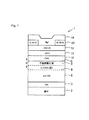
- 少なくとも、光吸収層(5)の表面(6)に隣接する領域において、少なくとも一つのアルカリ金属によってドープされた、光吸収層と
前記光吸収層(5)の前記表面(6)上の酸化不動態層(8)と
を含む、薄膜太陽電池のための層構造であって、
前記酸化不動態層は、前記光吸収層を腐食から保護するよう設計されている、層構造。 - 前記表面(6)上の前記酸化不動態層(8)が前記光吸収層(5)に組み込まれ、前記光吸収層の前記表面が変換された、請求項1に記載の層構造。
- 前記光吸収層(5)は、式中0≦x,y≦1であるCu(In1−xGax)(Se1−ySy)2、及び/又は式中0≦x≦1であるCu2ZnSn(Se1−xSx)4を含む、請求項1又は2に記載の層構造。
- 前記光吸収層(5)の前記表面(6)に隣接する前記領域が、p−n逆転(9)を示すようにドープされた、請求項1〜3のいずれか一項に記載の層構造。
- 前記少なくとも一つのアルカリ金属がルビジウム及び/又はセシウムである、請求項1〜4のいずれか一項に記載の層構造。
- 前記酸化不動態層(8)が、(In,Ga)2O3、式中M=K、Rb、Cs、かつ0<x,y,zであるMx(In,Ga)yOz、及び/又はAl2O3、及び/又はZnO、式中x=1〜2であるSnOxを含む、請求項1〜5のいずれか一項に記載の層構造。
- 前記酸化不動態層(8)の厚み(D)が1nm〜50nmである、請求項1〜6のいずれか一項に記載の層構造。
- 前記酸化不動態層(8)が、適用された緩衝層(10)を有する、請求項1〜7のいずれか一項に記載の層構造。
- 請求項1〜8のいずれか一項に記載の薄膜太陽電池のための層構造を製造する方法であって、前記方法は:
a.少なくとも、光吸収層(5)の表面(6)に隣接する領域に、少なくとも一つのアルカリ金属によってドープされた光吸収層を基材上に生成することと、
b.前記光吸収層の前記表面上に酸化不動態層(8)を生成することであって、前記酸化不動態層は、前記光吸収層を腐食から保護するよう設計されている、ことと
を含む、方法。 - 工程bは、前記光吸収層(5)の前記表面(6)が変換されるように、前記光吸収層に組み込まれた前記表面上の前記酸化不動態層(8)を含む、請求項9に記載の方法。
- 工程aが、以下のサブステップ:
ax.前記光吸収層(5)を生成することと
az.少なくとも、前記光吸収層の前記表面(6)に隣接する領域において、少なくとも一つのアルカリ金属で前記光吸収層をドープすることと
を含む、請求項9又は10に記載の方法。 - 前記光吸収層(5)の前記表面(6)に少なくとも一つのアルカリ金属を適用する工程であって、好ましくはSe雰囲気及び/又はS雰囲気下で、少なくとも一つのアルカリ金属を、少なくとも、前記光吸収層の前記表面に隣接する領域の内部へと内向きに拡散させることを含む工程azによって特徴付けられる、請求項11に記載の方法。
- 工程bが、アルカリ金属のドーピングを有する光吸収層(5)を、酸素を含む雰囲気中で、室温に対して高い温度でアニーリングすることを含み、前記酸化不動態層(8)は、好ましくは前記光吸収層及び酸素から生成される、請求項9〜12のいずれか一項に記載の方法。
- 工程bは、アルカリ金属のドーピングを有する前記光吸収層(5)の前記表面(6)に酸化物を適用することを含む、請求項9〜13のいずれか一項に記載の方法。
- 前記緩衝層(10)を前記酸化不動態層(8)に適用する工程によって特徴付けられる、請求項9〜14のいずれか一項に記載の方法。
Applications Claiming Priority (3)
| Application Number | Priority Date | Filing Date | Title |
|---|---|---|---|
| DE102014223485.9 | 2014-11-18 | ||
| DE102014223485.9A DE102014223485A1 (de) | 2014-11-18 | 2014-11-18 | Schichtaufbau für eine Dünnschichtsolarzelle und Herstellungsverfahren |
| PCT/EP2015/076996 WO2016079198A1 (de) | 2014-11-18 | 2015-11-18 | Schichtaufbau für eine dünnschichtsolarzelle und herstellungsverfahren |
Publications (2)
| Publication Number | Publication Date |
|---|---|
| JP2017534181A true JP2017534181A (ja) | 2017-11-16 |
| JP6662874B2 JP6662874B2 (ja) | 2020-03-11 |
Family
ID=54608517
Family Applications (1)
| Application Number | Title | Priority Date | Filing Date |
|---|---|---|---|
| JP2017525794A Active JP6662874B2 (ja) | 2014-11-18 | 2015-11-18 | 薄膜太陽電池のための層構造及びその製造方法 |
Country Status (6)
| Country | Link |
|---|---|
| US (1) | US11024758B2 (ja) |
| EP (1) | EP3221899B1 (ja) |
| JP (1) | JP6662874B2 (ja) |
| CN (1) | CN107112377B (ja) |
| DE (1) | DE102014223485A1 (ja) |
| WO (1) | WO2016079198A1 (ja) |
Cited By (2)
| Publication number | Priority date | Publication date | Assignee | Title |
|---|---|---|---|---|
| JP2019134151A (ja) * | 2018-01-29 | 2019-08-08 | ベイジン アポロ ディン ロン ソーラー テクノロジー カンパニー リミテッド | 薄膜太陽電池 |
| KR20210050564A (ko) * | 2018-09-22 | 2021-05-07 | (씨엔비엠) 벵부 디자인 앤드 리서치 인스티튜트 포 글래스 인더스트리 컴퍼니 리미티드 | 흡수체층의 후처리 방법 |
Families Citing this family (1)
| Publication number | Priority date | Publication date | Assignee | Title |
|---|---|---|---|---|
| CN207834314U (zh) * | 2018-06-08 | 2018-09-07 | 汉能新材料科技有限公司 | 太阳能电池 |
Citations (5)
| Publication number | Priority date | Publication date | Assignee | Title |
|---|---|---|---|---|
| US20110192454A1 (en) * | 2010-02-09 | 2011-08-11 | Feist Rebekah K | Photovoltaic device with transparent, conductive barrier layer |
| US20120024366A1 (en) * | 2010-07-27 | 2012-02-02 | National Taiwan University | Thin film solar cell structure and fabricating method thereof |
| US20120132281A1 (en) * | 2010-11-26 | 2012-05-31 | Nexpower Technology Corporation | Thin-film solar cell and manufacturing method thereof |
| JP2013118265A (ja) * | 2011-12-02 | 2013-06-13 | Showa Shell Sekiyu Kk | 薄膜太陽電池 |
| US20140124011A1 (en) * | 2011-09-09 | 2014-05-08 | International Business Machines Corporation | Heat Treatment Process and Photovoltaic Device Based on Said Process |
Family Cites Families (14)
| Publication number | Priority date | Publication date | Assignee | Title |
|---|---|---|---|---|
| EP0460287A1 (de) | 1990-05-31 | 1991-12-11 | Siemens Aktiengesellschaft | Neuartige Chalkopyrit-Solarzelle |
| DE4440878C2 (de) * | 1994-11-16 | 1999-04-29 | Zsw | Verbindungshalbleiter-Dünnschichtsolarzelle und Verfahren zu ihrer Herstellung |
| US6259016B1 (en) | 1999-03-05 | 2001-07-10 | Matsushita Electric Industrial Co., Ltd. | Solar cell |
| EP1273048B8 (en) * | 2000-04-06 | 2013-10-02 | HyET Energy Systems B.V. | Method of manufacturing a photovoltaic foil |
| US20040084079A1 (en) * | 2002-09-04 | 2004-05-06 | Ralph Romero | Photovoltaic device and module |
| DE102008045522A1 (de) | 2008-09-03 | 2010-03-04 | Fraunhofer-Gesellschaft zur Förderung der angewandten Forschung e.V. | Heterosolarzelle und Verfahren zur Herstellung von Heterosolarzellen |
| JP5229901B2 (ja) * | 2009-03-09 | 2013-07-03 | 富士フイルム株式会社 | 光電変換素子、及び太陽電池 |
| US8709856B2 (en) * | 2009-03-09 | 2014-04-29 | Zetta Research and Development LLC—AQT Series | Enhancement of semiconducting photovoltaic absorbers by the addition of alkali salts through solution coating techniques |
| JP5275950B2 (ja) * | 2009-05-01 | 2013-08-28 | 富士フイルム株式会社 | 積層膜とその製造方法、光電変換素子とその製造方法、及び太陽電池 |
| US20120055554A1 (en) * | 2009-05-21 | 2012-03-08 | E.I. Du Pont De Nemours And Company | Copper zinc tin chalcogenide nanoparticles |
| FR2982422B1 (fr) * | 2011-11-09 | 2013-11-15 | Saint Gobain | Substrat conducteur pour cellule photovoltaique |
| WO2013106836A1 (en) * | 2012-01-13 | 2013-07-18 | The Regents Of The University Of California | Metal-chalcogenide photovoltaic device with metal-oxide nanoparticle window layer |
| DE102012211894A1 (de) | 2012-07-09 | 2014-01-09 | Robert Bosch Gmbh | Verwendung von mikroporösen anionischen anorganischen Gerüststrukturen, insbesondere enthaltend Dotierstoffkationen, für die Herstellung von Dünnschichtsolarzellen bzw. -modulen, photovoltaische Dünnschichtsolarzellen, enthaltend mikroporöse anionische anorganische Gerüststrukturen sowie Verfahren zur Herstellung solcher photovoltaischen Dünnschichtsolarmodule |
| TWI654771B (zh) | 2012-12-21 | 2019-03-21 | 瑞士商弗里松股份有限公司 | 附加著鉀之薄膜光電裝置的製造 |
-
2014
- 2014-11-18 DE DE102014223485.9A patent/DE102014223485A1/de not_active Ceased
-
2015
- 2015-11-18 JP JP2017525794A patent/JP6662874B2/ja active Active
- 2015-11-18 WO PCT/EP2015/076996 patent/WO2016079198A1/de not_active Ceased
- 2015-11-18 CN CN201580062144.2A patent/CN107112377B/zh active Active
- 2015-11-18 EP EP15797653.1A patent/EP3221899B1/de active Active
- 2015-11-18 US US15/527,392 patent/US11024758B2/en active Active
Patent Citations (5)
| Publication number | Priority date | Publication date | Assignee | Title |
|---|---|---|---|---|
| US20110192454A1 (en) * | 2010-02-09 | 2011-08-11 | Feist Rebekah K | Photovoltaic device with transparent, conductive barrier layer |
| US20120024366A1 (en) * | 2010-07-27 | 2012-02-02 | National Taiwan University | Thin film solar cell structure and fabricating method thereof |
| US20120132281A1 (en) * | 2010-11-26 | 2012-05-31 | Nexpower Technology Corporation | Thin-film solar cell and manufacturing method thereof |
| US20140124011A1 (en) * | 2011-09-09 | 2014-05-08 | International Business Machines Corporation | Heat Treatment Process and Photovoltaic Device Based on Said Process |
| JP2013118265A (ja) * | 2011-12-02 | 2013-06-13 | Showa Shell Sekiyu Kk | 薄膜太陽電池 |
Cited By (4)
| Publication number | Priority date | Publication date | Assignee | Title |
|---|---|---|---|---|
| JP2019134151A (ja) * | 2018-01-29 | 2019-08-08 | ベイジン アポロ ディン ロン ソーラー テクノロジー カンパニー リミテッド | 薄膜太陽電池 |
| KR20210050564A (ko) * | 2018-09-22 | 2021-05-07 | (씨엔비엠) 벵부 디자인 앤드 리서치 인스티튜트 포 글래스 인더스트리 컴퍼니 리미티드 | 흡수체층의 후처리 방법 |
| JP2022501825A (ja) * | 2018-09-22 | 2022-01-06 | (シーエヌビーエム)ボンブー デザイン アンド リサーチ インスティテュート フォー グラス インダストリー カンパニー,リミティド | 吸収層を後処理する方法 |
| KR102594725B1 (ko) | 2018-09-22 | 2023-10-27 | 씨엔비엠 리서치 인스티튜트 포 어드밴스드 글래스 머터리얼즈 그룹 컴퍼니 리미티드 | 흡수체층의 후처리 방법 |
Also Published As
| Publication number | Publication date |
|---|---|
| CN107112377A (zh) | 2017-08-29 |
| EP3221899B1 (de) | 2023-07-12 |
| US11024758B2 (en) | 2021-06-01 |
| WO2016079198A1 (de) | 2016-05-26 |
| CN107112377B (zh) | 2020-06-19 |
| EP3221899A1 (de) | 2017-09-27 |
| US20170323984A1 (en) | 2017-11-09 |
| JP6662874B2 (ja) | 2020-03-11 |
| DE102014223485A1 (de) | 2016-05-19 |
Similar Documents
| Publication | Publication Date | Title |
|---|---|---|
| JP6096790B2 (ja) | 光電池のための導電性基材 | |
| JP5928612B2 (ja) | 化合物半導体太陽電池 | |
| JP2016541124A (ja) | 薄膜太陽電池用層系 | |
| WO2014171458A1 (ja) | 太陽電池及び太陽電池の製造方法 | |
| JP5654425B2 (ja) | 太陽電池 | |
| CN104051550A (zh) | 光伏器件及其制造方法 | |
| JP2011129631A (ja) | Cis系薄膜太陽電池の製造方法 | |
| CN104051565B (zh) | 制造光伏器件的方法 | |
| TWI492408B (zh) | 薄膜光伏元件的形成方法與cigs太陽能電池結構 | |
| JP6662874B2 (ja) | 薄膜太陽電池のための層構造及びその製造方法 | |
| TWI509821B (zh) | 光伏元件與其製作方法 | |
| CN103003959A (zh) | 半导体膜以及太阳能电池 | |
| US11557690B2 (en) | Semitransparent chalcogen solar cell | |
| US20250063848A1 (en) | Cadmium Selenide Based Photovoltaic Devices And Methods For Forming The Same | |
| TWI600176B (zh) | 化合物太陽能電池以及光吸收層的製作方法 | |
| TWI751520B (zh) | Pn接面及其製備方法及用途 | |
| TWI462319B (zh) | 堆疊式銅鋅錫硒硫薄膜太陽能電池及其製作方法 | |
| JP2014239122A (ja) | p型半導体膜及び光電素子 | |
| WO2024077583A1 (en) | Cdte based thin film solar cell device with diffusion barrier layer and method for manufacturing thereof | |
| JP2017017129A (ja) | 光電変換素子 | |
| US20140290730A1 (en) | Method of manufacturing thin film solar cell and thin film solar cell manufactured by the method | |
| JP5575163B2 (ja) | Cis系薄膜太陽電池の製造方法 | |
| JP2014107558A (ja) | 太陽電池、及び太陽電池の製造方法 | |
| US20210210645A1 (en) | Chalcogenide solar cell having transparent conducting oxide back contact, and method of manufacturing the chalcogenide solar cell | |
| WO2017043596A1 (ja) | 光電変換素子 |
Legal Events
| Date | Code | Title | Description |
|---|---|---|---|
| A621 | Written request for application examination |
Free format text: JAPANESE INTERMEDIATE CODE: A621 Effective date: 20171220 |
|
| A977 | Report on retrieval |
Free format text: JAPANESE INTERMEDIATE CODE: A971007 Effective date: 20181031 |
|
| A131 | Notification of reasons for refusal |
Free format text: JAPANESE INTERMEDIATE CODE: A131 Effective date: 20181204 |
|
| A521 | Request for written amendment filed |
Free format text: JAPANESE INTERMEDIATE CODE: A523 Effective date: 20190304 |
|
| A131 | Notification of reasons for refusal |
Free format text: JAPANESE INTERMEDIATE CODE: A131 Effective date: 20190910 |
|
| A521 | Request for written amendment filed |
Free format text: JAPANESE INTERMEDIATE CODE: A523 Effective date: 20191210 |
|
| TRDD | Decision of grant or rejection written | ||
| A01 | Written decision to grant a patent or to grant a registration (utility model) |
Free format text: JAPANESE INTERMEDIATE CODE: A01 Effective date: 20200114 |
|
| A61 | First payment of annual fees (during grant procedure) |
Free format text: JAPANESE INTERMEDIATE CODE: A61 Effective date: 20200213 |
|
| R150 | Certificate of patent or registration of utility model |
Ref document number: 6662874 Country of ref document: JP Free format text: JAPANESE INTERMEDIATE CODE: R150 |
|
| R250 | Receipt of annual fees |
Free format text: JAPANESE INTERMEDIATE CODE: R250 |
|
| R250 | Receipt of annual fees |
Free format text: JAPANESE INTERMEDIATE CODE: R250 |
|
| R250 | Receipt of annual fees |
Free format text: JAPANESE INTERMEDIATE CODE: R250 |