JP2018169587A - 光走査装置、画像形成装置、異常検出方法 - Google Patents
光走査装置、画像形成装置、異常検出方法 Download PDFInfo
- Publication number
- JP2018169587A JP2018169587A JP2017069066A JP2017069066A JP2018169587A JP 2018169587 A JP2018169587 A JP 2018169587A JP 2017069066 A JP2017069066 A JP 2017069066A JP 2017069066 A JP2017069066 A JP 2017069066A JP 2018169587 A JP2018169587 A JP 2018169587A
- Authority
- JP
- Japan
- Prior art keywords
- speed
- motor
- control unit
- temperature
- abnormal state
- Prior art date
- Legal status (The legal status is an assumption and is not a legal conclusion. Google has not performed a legal analysis and makes no representation as to the accuracy of the status listed.)
- Granted
Links
Images

Classifications
-
- G—PHYSICS
- G02—OPTICS
- G02B—OPTICAL ELEMENTS, SYSTEMS OR APPARATUS
- G02B26/00—Optical devices or arrangements for the control of light using movable or deformable optical elements
- G02B26/08—Optical devices or arrangements for the control of light using movable or deformable optical elements for controlling the direction of light
- G02B26/10—Scanning systems
- G02B26/12—Scanning systems using multifaceted mirrors
-
- G—PHYSICS
- G03—PHOTOGRAPHY; CINEMATOGRAPHY; ANALOGOUS TECHNIQUES USING WAVES OTHER THAN OPTICAL WAVES; ELECTROGRAPHY; HOLOGRAPHY
- G03G—ELECTROGRAPHY; ELECTROPHOTOGRAPHY; MAGNETOGRAPHY
- G03G15/00—Apparatus for electrographic processes using a charge pattern
- G03G15/04—Apparatus for electrographic processes using a charge pattern for exposing, i.e. imagewise exposure by optically projecting the original image on a photoconductive recording material
- G03G15/04036—Details of illuminating systems, e.g. lamps, reflectors
- G03G15/04045—Details of illuminating systems, e.g. lamps, reflectors for exposing image information provided otherwise than by directly projecting the original image onto the photoconductive recording material, e.g. digital copiers
- G03G15/04072—Details of illuminating systems, e.g. lamps, reflectors for exposing image information provided otherwise than by directly projecting the original image onto the photoconductive recording material, e.g. digital copiers by laser
-
- G—PHYSICS
- G02—OPTICS
- G02B—OPTICAL ELEMENTS, SYSTEMS OR APPARATUS
- G02B26/00—Optical devices or arrangements for the control of light using movable or deformable optical elements
- G02B26/08—Optical devices or arrangements for the control of light using movable or deformable optical elements for controlling the direction of light
- G02B26/10—Scanning systems
- G02B26/12—Scanning systems using multifaceted mirrors
- G02B26/121—Mechanical drive devices for polygonal mirrors
- G02B26/122—Control of the scanning speed of the polygonal mirror
-
- G—PHYSICS
- G03—PHOTOGRAPHY; CINEMATOGRAPHY; ANALOGOUS TECHNIQUES USING WAVES OTHER THAN OPTICAL WAVES; ELECTROGRAPHY; HOLOGRAPHY
- G03G—ELECTROGRAPHY; ELECTROPHOTOGRAPHY; MAGNETOGRAPHY
- G03G15/00—Apparatus for electrographic processes using a charge pattern
- G03G15/04—Apparatus for electrographic processes using a charge pattern for exposing, i.e. imagewise exposure by optically projecting the original image on a photoconductive recording material
- G03G15/0409—Details of projection optics
-
- G—PHYSICS
- G03—PHOTOGRAPHY; CINEMATOGRAPHY; ANALOGOUS TECHNIQUES USING WAVES OTHER THAN OPTICAL WAVES; ELECTROGRAPHY; HOLOGRAPHY
- G03G—ELECTROGRAPHY; ELECTROPHOTOGRAPHY; MAGNETOGRAPHY
- G03G15/00—Apparatus for electrographic processes using a charge pattern
- G03G15/04—Apparatus for electrographic processes using a charge pattern for exposing, i.e. imagewise exposure by optically projecting the original image on a photoconductive recording material
- G03G15/043—Apparatus for electrographic processes using a charge pattern for exposing, i.e. imagewise exposure by optically projecting the original image on a photoconductive recording material with means for controlling illumination or exposure
-
- G—PHYSICS
- G03—PHOTOGRAPHY; CINEMATOGRAPHY; ANALOGOUS TECHNIQUES USING WAVES OTHER THAN OPTICAL WAVES; ELECTROGRAPHY; HOLOGRAPHY
- G03G—ELECTROGRAPHY; ELECTROPHOTOGRAPHY; MAGNETOGRAPHY
- G03G15/00—Apparatus for electrographic processes using a charge pattern
- G03G15/55—Self-diagnostics; Malfunction or lifetime display
-
- G—PHYSICS
- G03—PHOTOGRAPHY; CINEMATOGRAPHY; ANALOGOUS TECHNIQUES USING WAVES OTHER THAN OPTICAL WAVES; ELECTROGRAPHY; HOLOGRAPHY
- G03G—ELECTROGRAPHY; ELECTROPHOTOGRAPHY; MAGNETOGRAPHY
- G03G21/00—Arrangements not provided for by groups G03G13/00 - G03G19/00, e.g. cleaning, elimination of residual charge
- G03G21/20—Humidity or temperature control also ozone evacuation; Internal apparatus environment control
-
- G—PHYSICS
- G05—CONTROLLING; REGULATING
- G05D—SYSTEMS FOR CONTROLLING OR REGULATING NON-ELECTRIC VARIABLES
- G05D23/00—Control of temperature
- G05D23/19—Control of temperature characterised by the use of electric means
-
- G—PHYSICS
- G06—COMPUTING OR CALCULATING; COUNTING
- G06K—GRAPHICAL DATA READING; PRESENTATION OF DATA; RECORD CARRIERS; HANDLING RECORD CARRIERS
- G06K15/00—Arrangements for producing a permanent visual presentation of the output data, e.g. computer output printers
- G06K15/02—Arrangements for producing a permanent visual presentation of the output data, e.g. computer output printers using printers
- G06K15/12—Arrangements for producing a permanent visual presentation of the output data, e.g. computer output printers using printers by photographic printing, e.g. by laser printers
- G06K15/1204—Arrangements for producing a permanent visual presentation of the output data, e.g. computer output printers using printers by photographic printing, e.g. by laser printers involving the fast moving of an optical beam in the main scanning direction
-
- G—PHYSICS
- G03—PHOTOGRAPHY; CINEMATOGRAPHY; ANALOGOUS TECHNIQUES USING WAVES OTHER THAN OPTICAL WAVES; ELECTROGRAPHY; HOLOGRAPHY
- G03G—ELECTROGRAPHY; ELECTROPHOTOGRAPHY; MAGNETOGRAPHY
- G03G2215/00—Apparatus for electrophotographic processes
- G03G2215/04—Arrangements for exposing and producing an image
- G03G2215/0402—Exposure devices
- G03G2215/0404—Laser
Landscapes
- Physics & Mathematics (AREA)
- General Physics & Mathematics (AREA)
- Optics & Photonics (AREA)
- Engineering & Computer Science (AREA)
- Ecology (AREA)
- Environmental & Geological Engineering (AREA)
- Environmental Sciences (AREA)
- Life Sciences & Earth Sciences (AREA)
- Atmospheric Sciences (AREA)
- Biodiversity & Conservation Biology (AREA)
- General Engineering & Computer Science (AREA)
- Theoretical Computer Science (AREA)
- Automation & Control Theory (AREA)
- Control Or Security For Electrophotography (AREA)
- Mechanical Optical Scanning Systems (AREA)
- Facsimile Scanning Arrangements (AREA)
- Control Of Electric Motors In General (AREA)
- Laser Beam Printer (AREA)
- Exposure Or Original Feeding In Electrophotography (AREA)
- Microelectronics & Electronic Packaging (AREA)
Abstract
Description
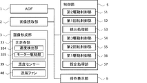
まず、図1及び図2を参照しつつ、本発明の実施形態に係る画像形成装置10の概略構成について説明する。ここで、図1は画像形成装置10の構成を示す断面模式図である。
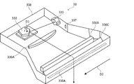
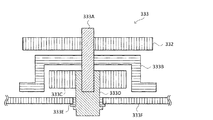
次に、図2〜図4を参照しつつ、光走査部33について説明する。ここで、図3は光走査部33の構成を示す斜視図である。また、図4はモーター333の構成を示す断面模式図である。
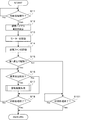
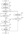
以下、図5を参照しつつ、画像形成装置10において制御部5により実行される異常検出処理の手順の一例について説明する。ここで、ステップS11、S12・・・は、制御部5により実行される処理手順(ステップ)の番号を表している。
まず、ステップS11において、制御部5は、前記印刷処理の実行指示が入力されたか否かを判断する。
ステップS12において、制御部5は、温度センサー39によって検出される温度に基づいて、現像部34の現像ローラー341に印加される前記現像バイアス電圧を設定する。ここで、ステップS12の処理は、制御部5の設定処理部57によって実行される。
ステップS13において、制御部5は、モーター333を駆動させる。ここで、ステップS13の処理は、制御部5の第2駆動制御部51によって実行される。
ステップS14において、制御部5は、送風ファン40を前記第3速度で回転させる。ここで、ステップS14の処理は、制御部5の第1回転制御部52により実行される。
ステップS15において、制御部5は、モーター333が前記第1速度で駆動されているか否かを判断する。
ステップS151において、制御部5は、ステップS11で実行指示が入力された前記印刷処理が終了したか否かを判断する。
ステップS16において、制御部5は、軸受部333Dから前記第1範囲内で検出される気温に基づいて、軸受部333Dの温度が前記許容温度を超える前記異常状態が検出されたか否かを判断する。ここで、ステップS15〜S16の処理は、制御部5の検出処理部53によって実行される。
ステップS17において、制御部5は、後述する駆動制限処理を実行する。
ステップS18において、制御部5は、ステップS11で実行指示が入力された前記印刷処理が終了したか否かを判断する。
次に、図6を参照しつつ、前記異常検出処理のステップS17で実行される駆動制限処理の手順の一例を説明する。
まず、ステップS21において、制御部5は、送風ファン40を前記第3速度より速い前記第4速度で回転させる。ここで、ステップS21の処理は、制御部5の第2回転制御部55によって実行される。
ステップS22において、制御部5は、モーター333の駆動速度の変更操作を受け付けるための受付画面を操作表示部6に表示させる。これにより、ユーザーは、前記印刷処理ごとに、モーター333の駆動速度を低下させて前記印刷処理を継続するか、もしくは前記印刷処理を中断するかを選択可能である。特に、画像形成装置10のように、モーター333の駆動速度の変更によって印刷物の画質が低下する場合に、ユーザーの意に反して画質の低い印刷物が出力されることを回避可能である。
ステップS23において、制御部5は、ステップS22で操作表示部6に表示された前記受付画面において、モーター333の駆動速度の変更操作が受け付けられたか否かを判断する。
ステップS231において、制御部5は、モーター333の駆動速度を前記第2速度に変更する。ここで、ステップS22、ステップS23、及びステップS231の処理は、制御部5の第3駆動制御部54によって実行される。
ステップS232において、制御部5は、前記停止条件を充足したか否かを判断する。
ステップS24において、制御部5は、前記異常検出処理のステップS11で実行指示が入力された前記印刷処理において印刷物が出力された後であるか否かを判断する。
ステップS25において、制御部5は、モーター333の駆動を停止させる。ここで、ステップS24、及びステップS25の処理は、制御部5の第1駆動制御部56によって実行される。
ステップS26において、制御部5は、前記再開条件を充足したか否かを判断する。
ステップS27において、制御部5は、モーター333の駆動を再開させる。
2 :画像読取部
3 :画像形成部
4 :給紙部
5 :制御部
6 :操作表示部
10 :画像形成装置
31 :感光体ドラム
32 :帯電部材
33 :光走査部
34 :現像部
35 :転写ローラー
36 :クリーニング装置
37 :定着装置
39 :温度センサー
40 :送風ファン
51 :第2駆動制御部
52 :第1回転制御部
53 :検出処理部
54 :第3駆動制御部
55 :第2回転制御部
56 :第1駆動制御部
57 :設定処理部
331:光源
332:ポリゴンミラー
333:モーター
333A:回転軸
333D:軸受部
338:ハウジング
341:現像ローラー
Claims (13)
- 光源から射出される光を走査させる回転多面鏡と、
前記回転多面鏡を回転させるモーターと、
前記モーターの回転軸を回転可能に支持する軸受部と、
前記モーターが予め定められた基準速度より速い第1速度で駆動される場合は、前記軸受部から予め定められた第1範囲内で検出される気温に基づいて前記軸受部の温度が予め設定された許容温度を超える異常状態を検出し、前記モーターが前記基準速度以下の第2速度で駆動される場合は、前記異常状態を検出しない検出処理部と、
を備える光走査装置。 - 前記検出処理部は、前記気温が予め定められた第1閾値を超える場合に前記異常状態を検出する、
請求項1に記載の光走査装置。 - 前記検出処理部は、前記気温の上昇速度が予め定められた第2閾値を超える場合に前記異常状態を検出する、
請求項1に記載の光走査装置。 - 請求項1〜3のいずれかに記載の光走査装置を備える画像形成装置。
- 前記検出処理部によって前記異常状態が検出された場合に、前記モーターの駆動を予め定められた再開条件を充足するまでの間停止させる第1駆動制御部を備える、
請求項4に記載の画像形成装置。 - シートに画像を形成する印刷処理が実行される場合に前記モーターを駆動させる第2駆動制御部を備え、
前記第1駆動制御部は、前記検出処理部によって前記異常状態が検出された場合に、少なくとも1枚の印刷物が出力された後に前記モーターの駆動を停止させる、
請求項5に記載の画像形成装置。 - 前記検出処理部によって前記異常状態が検出された場合に、前記モーターの駆動速度を前記第1速度から前記第2速度に変更可能な第3駆動制御部を備え、
前記第1駆動制御部は、前記第3駆動制御部によって前記駆動速度が前記第2速度に変更されない場合に、前記モーターの駆動を停止させる、
請求項5又は6に記載の画像形成装置。 - 前記第3駆動制御部は、前記検出処理部による前記異常状態の検出後に受け付けられるユーザー操作に応じて、前記駆動速度を前記第2速度に変更する、
請求項7に記載の画像形成装置。 - 前記第1駆動制御部は、前記第3駆動制御部による前記駆動速度の変更後において予め定められた停止条件を充足する場合に、前記モーターの駆動を停止させる、
請求項7又は8に記載の画像形成装置。 - 前記検出処理部によって前記異常状態が検出された場合に、前記モーターの駆動速度を前記第1速度から前記第2速度に変更する第3駆動制御部を備える、
請求項4に記載の画像形成装置。 - 前記回転多面鏡、前記モーター、及び前記軸受部を収容するハウジングと、
前記ハウジングの外面に沿って移動する気流を発生させる送風ファンと、
前記送風ファンを予め定められた第3速度で回転させる第1回転制御部と、
前記検出処理部によって前記異常状態が検出された場合に、前記送風ファンを前記第3速度より速い第4速度で回転させる第2回転制御部と、
を備える請求項4〜10のいずれかに記載の画像形成装置。 - 像担持体にトナーを供給する現像ローラーを有し、前記像担持体に形成される静電潜像を現像する現像部と、
前記軸受部から前記第1範囲内であって且つ前記光走査装置と前記現像部との間に配置され、配置位置における温度を検出する温度センサーと、
前記温度センサーによって検出される温度に基づいて前記現像ローラーに印加される電圧を設定する設定処理部と、を備え、
前記検出処理部は、前記温度センサーによって検出される温度に基づいて前記異常状態を検出する、
請求項4〜11のいずれかに記載の画像形成装置。 - 光源から射出される光を走査させる回転多面鏡と、前記回転多面鏡を回転させるモーターと、前記モーターの回転軸を回転可能に支持する軸受部と、を備える光走査装置で実行される異常検出方法であって、
前記モーターを駆動させることと、
前記モーターが予め定められた基準速度より速い第1速度で駆動される場合は、前記軸受部から予め定められた第1範囲内で検出される気温に基づいて前記軸受部の温度が予め設定された許容温度を超える異常状態を検出し、前記モーターが前記基準速度以下の第2速度で駆動される場合は、前記異常状態を検出しないことと、
を含む異常検出方法。
Priority Applications (4)
| Application Number | Priority Date | Filing Date | Title |
|---|---|---|---|
| JP2017069066A JP6635082B2 (ja) | 2017-03-30 | 2017-03-30 | 光走査装置、画像形成装置、異常検出方法 |
| CN201810223887.9A CN108693640B (zh) | 2017-03-30 | 2018-03-19 | 图像形成装置和异常检测方法 |
| US15/926,733 US10289020B2 (en) | 2017-03-30 | 2018-03-20 | Laser scanning device capable of detecting abnormal state, image forming apparatus, abnormality detection method |
| EP18164259.6A EP3382458B1 (en) | 2017-03-30 | 2018-03-27 | Laser scanning device capable of detecting abnormal state, image forming apparatus, abnormality detection method |
Applications Claiming Priority (1)
| Application Number | Priority Date | Filing Date | Title |
|---|---|---|---|
| JP2017069066A JP6635082B2 (ja) | 2017-03-30 | 2017-03-30 | 光走査装置、画像形成装置、異常検出方法 |
Publications (2)
| Publication Number | Publication Date |
|---|---|
| JP2018169587A true JP2018169587A (ja) | 2018-11-01 |
| JP6635082B2 JP6635082B2 (ja) | 2020-01-22 |
Family
ID=61827610
Family Applications (1)
| Application Number | Title | Priority Date | Filing Date |
|---|---|---|---|
| JP2017069066A Expired - Fee Related JP6635082B2 (ja) | 2017-03-30 | 2017-03-30 | 光走査装置、画像形成装置、異常検出方法 |
Country Status (4)
| Country | Link |
|---|---|
| US (1) | US10289020B2 (ja) |
| EP (1) | EP3382458B1 (ja) |
| JP (1) | JP6635082B2 (ja) |
| CN (1) | CN108693640B (ja) |
Cited By (1)
| Publication number | Priority date | Publication date | Assignee | Title |
|---|---|---|---|---|
| US20250044719A1 (en) * | 2023-07-31 | 2025-02-06 | Kyocera Document Solutions Inc. | Image forming apparatus |
Families Citing this family (1)
| Publication number | Priority date | Publication date | Assignee | Title |
|---|---|---|---|---|
| JP7581082B2 (ja) * | 2021-02-26 | 2024-11-12 | キヤノン株式会社 | 画像形成装置 |
Citations (5)
| Publication number | Priority date | Publication date | Assignee | Title |
|---|---|---|---|---|
| JP2004212705A (ja) * | 2003-01-06 | 2004-07-29 | Konica Minolta Holdings Inc | 光偏向装置及び画像形成装置 |
| JP2004309526A (ja) * | 2003-04-02 | 2004-11-04 | Seiko Epson Corp | 画像形成装置および画像形成装置のファン制御方法 |
| JP2006095735A (ja) * | 2004-09-28 | 2006-04-13 | Brother Ind Ltd | 画像形成装置 |
| US9298160B1 (en) * | 2015-05-28 | 2016-03-29 | Kabushiki Kaisha Toshiba | Image forming apparatus and cooling control method for image forming apparatus |
| JP2016224270A (ja) * | 2015-05-29 | 2016-12-28 | 京セラドキュメントソリューションズ株式会社 | 画像形成装置、光走査装置、メンテナンス方法 |
Family Cites Families (13)
| Publication number | Priority date | Publication date | Assignee | Title |
|---|---|---|---|---|
| JPH1082965A (ja) * | 1996-09-05 | 1998-03-31 | Asahi Optical Co Ltd | 光走査装置および光走査方法 |
| JP2000089152A (ja) * | 1998-09-08 | 2000-03-31 | Ricoh Co Ltd | 光走査装置 |
| JP2001083451A (ja) * | 1999-09-13 | 2001-03-30 | Canon Inc | 画像形成装置 |
| JP3876775B2 (ja) | 2002-06-24 | 2007-02-07 | ブラザー工業株式会社 | プリンタ |
| JP4091885B2 (ja) * | 2003-08-05 | 2008-05-28 | 株式会社リコー | 軸受異常検出装置、軸受異常検出方法、画像形成装置及びディスクドライブ装置 |
| JP2006126578A (ja) * | 2004-10-29 | 2006-05-18 | Canon Inc | 画像形成装置 |
| JP5380204B2 (ja) * | 2009-08-24 | 2014-01-08 | 京セラドキュメントソリューションズ株式会社 | 画像形成装置 |
| JP2011123332A (ja) * | 2009-12-11 | 2011-06-23 | Ricoh Co Ltd | 画像形成装置、温度測定方法および温度測定装置 |
| JP5423733B2 (ja) * | 2011-07-07 | 2014-02-19 | コニカミノルタ株式会社 | 画像形成装置および画像形成装置の制御方法 |
| JP5340439B2 (ja) * | 2012-02-27 | 2013-11-13 | 京セラドキュメントソリューションズ株式会社 | 画像形成装置 |
| JP6265690B2 (ja) * | 2013-11-08 | 2018-01-24 | キヤノン株式会社 | 画像形成装置 |
| JP6365442B2 (ja) * | 2015-06-29 | 2018-08-01 | 京セラドキュメントソリューションズ株式会社 | 光走査装置、画像形成装置、光走査方法 |
| JP6100329B2 (ja) * | 2015-07-27 | 2017-03-22 | キヤノン株式会社 | 画像形成装置 |
-
2017
- 2017-03-30 JP JP2017069066A patent/JP6635082B2/ja not_active Expired - Fee Related
-
2018
- 2018-03-19 CN CN201810223887.9A patent/CN108693640B/zh not_active Expired - Fee Related
- 2018-03-20 US US15/926,733 patent/US10289020B2/en active Active
- 2018-03-27 EP EP18164259.6A patent/EP3382458B1/en not_active Not-in-force
Patent Citations (5)
| Publication number | Priority date | Publication date | Assignee | Title |
|---|---|---|---|---|
| JP2004212705A (ja) * | 2003-01-06 | 2004-07-29 | Konica Minolta Holdings Inc | 光偏向装置及び画像形成装置 |
| JP2004309526A (ja) * | 2003-04-02 | 2004-11-04 | Seiko Epson Corp | 画像形成装置および画像形成装置のファン制御方法 |
| JP2006095735A (ja) * | 2004-09-28 | 2006-04-13 | Brother Ind Ltd | 画像形成装置 |
| US9298160B1 (en) * | 2015-05-28 | 2016-03-29 | Kabushiki Kaisha Toshiba | Image forming apparatus and cooling control method for image forming apparatus |
| JP2016224270A (ja) * | 2015-05-29 | 2016-12-28 | 京セラドキュメントソリューションズ株式会社 | 画像形成装置、光走査装置、メンテナンス方法 |
Cited By (2)
| Publication number | Priority date | Publication date | Assignee | Title |
|---|---|---|---|---|
| US20250044719A1 (en) * | 2023-07-31 | 2025-02-06 | Kyocera Document Solutions Inc. | Image forming apparatus |
| US12601988B2 (en) * | 2023-07-31 | 2026-04-14 | Kyocera Document Solutions Inc. | Image forming apparatus |
Also Published As
| Publication number | Publication date |
|---|---|
| CN108693640A (zh) | 2018-10-23 |
| EP3382458B1 (en) | 2020-10-14 |
| EP3382458A1 (en) | 2018-10-03 |
| JP6635082B2 (ja) | 2020-01-22 |
| CN108693640B (zh) | 2021-02-19 |
| US10289020B2 (en) | 2019-05-14 |
| US20180284680A1 (en) | 2018-10-04 |
Similar Documents
| Publication | Publication Date | Title |
|---|---|---|
| US8941701B2 (en) | Image forming apparatus and method for controlling the image forming apparatus | |
| JP6398876B2 (ja) | 画像形成装置、光走査装置、メンテナンス方法 | |
| JP6124137B2 (ja) | 画像形成装置 | |
| JP6635082B2 (ja) | 光走査装置、画像形成装置、異常検出方法 | |
| JP2006133310A (ja) | 画像形成装置及び画像形成方法 | |
| JP5380204B2 (ja) | 画像形成装置 | |
| JP2018032000A (ja) | 光走査装置、画像形成装置、反射面識別方法 | |
| JP2005134449A (ja) | 画像形成装置及びその制御方法 | |
| JP2018069518A (ja) | 光走査装置、画像形成装置、光量制御方法 | |
| JP6579072B2 (ja) | 光走査装置、画像形成装置、反射面識別方法 | |
| JP6446956B2 (ja) | 画像形成装置、その制御方法、および、コンピュータプログラム | |
| JP7534903B2 (ja) | 画像形成装置 | |
| JPH07181830A (ja) | 画像形成装置 | |
| JP5929392B2 (ja) | 画像形成装置 | |
| JP2005049621A (ja) | 画像形成装置,その制御方法 | |
| JP2008026792A (ja) | 画像形成装置 | |
| JPH0519558A (ja) | 画像形成装置 | |
| JP2002351241A (ja) | 画像形成装置 | |
| JP4338474B2 (ja) | 定着装置,画像形成装置,定着装置の制御方法 | |
| US20070216758A1 (en) | Driving control device, image forming apparatus and recording medium for recording driving control program | |
| WO2018079336A1 (ja) | 光走査装置、画像形成装置、反射面識別方法 | |
| JP2018072552A (ja) | 光走査装置、画像形成装置、駆動制御方法 | |
| JP2016071105A (ja) | 画像形成装置、その制御方法およびコンピュータプログラム | |
| JP2005266241A (ja) | 画像形成装置 | |
| JP6308164B2 (ja) | 画像形成装置 |
Legal Events
| Date | Code | Title | Description |
|---|---|---|---|
| A621 | Written request for application examination |
Free format text: JAPANESE INTERMEDIATE CODE: A621 Effective date: 20181227 |
|
| A977 | Report on retrieval |
Free format text: JAPANESE INTERMEDIATE CODE: A971007 Effective date: 20191023 |
|
| A131 | Notification of reasons for refusal |
Free format text: JAPANESE INTERMEDIATE CODE: A131 Effective date: 20191029 |
|
| A521 | Request for written amendment filed |
Free format text: JAPANESE INTERMEDIATE CODE: A523 Effective date: 20191031 |
|
| TRDD | Decision of grant or rejection written | ||
| A01 | Written decision to grant a patent or to grant a registration (utility model) |
Free format text: JAPANESE INTERMEDIATE CODE: A01 Effective date: 20191119 |
|
| A61 | First payment of annual fees (during grant procedure) |
Free format text: JAPANESE INTERMEDIATE CODE: A61 Effective date: 20191202 |
|
| R150 | Certificate of patent or registration of utility model |
Ref document number: 6635082 Country of ref document: JP Free format text: JAPANESE INTERMEDIATE CODE: R150 |
|
| LAPS | Cancellation because of no payment of annual fees |