JP2018517954A - Sensor-based NFC / RF mechanisms having multiple valid states for detecting opened or damaged containers and methods of making and using them - Google Patents
Sensor-based NFC / RF mechanisms having multiple valid states for detecting opened or damaged containers and methods of making and using them Download PDFInfo
- Publication number
- JP2018517954A JP2018517954A JP2017548281A JP2017548281A JP2018517954A JP 2018517954 A JP2018517954 A JP 2018517954A JP 2017548281 A JP2017548281 A JP 2017548281A JP 2017548281 A JP2017548281 A JP 2017548281A JP 2018517954 A JP2018517954 A JP 2018517954A
- Authority
- JP
- Japan
- Prior art keywords
- container
- package
- continuity
- sensor
- integrated circuit
- Prior art date
- Legal status (The legal status is an assumption and is not a legal conclusion. Google has not performed a legal analysis and makes no representation as to the accuracy of the status listed.)
- Pending
Links
Images


Classifications
-
- G—PHYSICS
- G08—SIGNALLING
- G08C—TRANSMISSION SYSTEMS FOR MEASURED VALUES, CONTROL OR SIMILAR SIGNALS
- G08C17/00—Arrangements for transmitting signals characterised by the use of a wireless electrical link
- G08C17/02—Arrangements for transmitting signals characterised by the use of a wireless electrical link using a radio link
-
- G—PHYSICS
- G01—MEASURING; TESTING
- G01M—TESTING STATIC OR DYNAMIC BALANCE OF MACHINES OR STRUCTURES; TESTING OF STRUCTURES OR APPARATUS, NOT OTHERWISE PROVIDED FOR
- G01M3/00—Investigating fluid-tightness of structures
- G01M3/02—Investigating fluid-tightness of structures by using fluid or vacuum
- G01M3/04—Investigating fluid-tightness of structures by using fluid or vacuum by detecting the presence of fluid at the leakage point
- G01M3/16—Investigating fluid-tightness of structures by using fluid or vacuum by detecting the presence of fluid at the leakage point using electric detection means
- G01M3/18—Investigating fluid-tightness of structures by using fluid or vacuum by detecting the presence of fluid at the leakage point using electric detection means for pipes, cables or tubes; for pipe joints or seals; for valves; for welds; for containers, e.g. radiators
- G01M3/186—Investigating fluid-tightness of structures by using fluid or vacuum by detecting the presence of fluid at the leakage point using electric detection means for pipes, cables or tubes; for pipe joints or seals; for valves; for welds; for containers, e.g. radiators for containers, e.g. radiators
- G01M3/187—Investigating fluid-tightness of structures by using fluid or vacuum by detecting the presence of fluid at the leakage point using electric detection means for pipes, cables or tubes; for pipe joints or seals; for valves; for welds; for containers, e.g. radiators for containers, e.g. radiators for flexible or elastic containers
-
- G—PHYSICS
- G01—MEASURING; TESTING
- G01N—INVESTIGATING OR ANALYSING MATERIALS BY DETERMINING THEIR CHEMICAL OR PHYSICAL PROPERTIES
- G01N33/00—Investigating or analysing materials by specific methods not covered by groups G01N1/00 - G01N31/00
- G01N33/0004—Gaseous mixtures, e.g. polluted air
- G01N33/0009—General constructional details of gas analysers, e.g. portable test equipment
- G01N33/0073—Control unit therefor
- G01N33/0075—Control unit therefor for multiple spatially distributed sensors, e.g. for environmental monitoring
-
- G—PHYSICS
- G06—COMPUTING OR CALCULATING; COUNTING
- G06Q—INFORMATION AND COMMUNICATION TECHNOLOGY [ICT] SPECIALLY ADAPTED FOR ADMINISTRATIVE, COMMERCIAL, FINANCIAL, MANAGERIAL OR SUPERVISORY PURPOSES; SYSTEMS OR METHODS SPECIALLY ADAPTED FOR ADMINISTRATIVE, COMMERCIAL, FINANCIAL, MANAGERIAL OR SUPERVISORY PURPOSES, NOT OTHERWISE PROVIDED FOR
- G06Q30/00—Commerce
- G06Q30/018—Certifying business or products
- G06Q30/0185—Product, service or business identity fraud
-
- G—PHYSICS
- G06—COMPUTING OR CALCULATING; COUNTING
- G06Q—INFORMATION AND COMMUNICATION TECHNOLOGY [ICT] SPECIALLY ADAPTED FOR ADMINISTRATIVE, COMMERCIAL, FINANCIAL, MANAGERIAL OR SUPERVISORY PURPOSES; SYSTEMS OR METHODS SPECIALLY ADAPTED FOR ADMINISTRATIVE, COMMERCIAL, FINANCIAL, MANAGERIAL OR SUPERVISORY PURPOSES, NOT OTHERWISE PROVIDED FOR
- G06Q30/00—Commerce
- G06Q30/06—Buying, selling or leasing transactions
- G06Q30/0601—Electronic shopping [e-shopping]
-
- H—ELECTRICITY
- H04—ELECTRIC COMMUNICATION TECHNIQUE
- H04Q—SELECTING
- H04Q9/00—Arrangements in telecontrol or telemetry systems for selectively calling a substation from a main station, in which substation desired apparatus is selected for applying a control signal thereto or for obtaining measured values therefrom
-
- H—ELECTRICITY
- H04—ELECTRIC COMMUNICATION TECHNIQUE
- H04Q—SELECTING
- H04Q2209/00—Arrangements in telecontrol or telemetry systems
- H04Q2209/40—Arrangements in telecontrol or telemetry systems using a wireless architecture
- H04Q2209/47—Arrangements in telecontrol or telemetry systems using a wireless architecture using RFID associated with sensors
Landscapes
- Business, Economics & Management (AREA)
- Engineering & Computer Science (AREA)
- Physics & Mathematics (AREA)
- General Physics & Mathematics (AREA)
- Finance (AREA)
- Accounting & Taxation (AREA)
- Theoretical Computer Science (AREA)
- Marketing (AREA)
- General Business, Economics & Management (AREA)
- Strategic Management (AREA)
- Economics (AREA)
- Development Economics (AREA)
- Chemical & Material Sciences (AREA)
- Entrepreneurship & Innovation (AREA)
- Health & Medical Sciences (AREA)
- Computer Networks & Wireless Communication (AREA)
- Life Sciences & Earth Sciences (AREA)
- General Health & Medical Sciences (AREA)
- Pathology (AREA)
- Biochemistry (AREA)
- Immunology (AREA)
- Analytical Chemistry (AREA)
- Combustion & Propulsion (AREA)
- Food Science & Technology (AREA)
- Medicinal Chemistry (AREA)
- Arrangements For Transmission Of Measured Signals (AREA)
- Toxicology (AREA)
- Computer Vision & Pattern Recognition (AREA)
- Microelectronics & Electronic Packaging (AREA)
- Artificial Intelligence (AREA)
- Electromagnetism (AREA)
- Electrochemistry (AREA)
- Chemical Kinetics & Catalysis (AREA)
- Molecular Biology (AREA)
- Computer Hardware Design (AREA)
- Computer Security & Cryptography (AREA)
- Details Of Rigid Or Semi-Rigid Containers (AREA)
- Near-Field Transmission Systems (AREA)
Abstract
ワイヤレス(例えば、近距離またはRF)通信デバイス、および、それらを製造および使用する方法が開示されている。ワイヤレス通信デバイスは、受信部および/または送信部、その上にアンテナを有する基板、集積回路、および、1または複数の導通センサを含む。アンテナは、ワイヤレス信号を受信および/もしくは送信、または、ブロードキャストする。集積回路は、ワイヤレス信号、および/もしくは、それらからの情報を処理し、ならびに/または、ワイヤレス信号、および/もしくは、それらのための情報を生成する。導通センサは、パッケージまたは容器内の化学薬品または物質の存在を検知または判定され、従って、通信デバイスが配置される、または通信デバイスが固定または固着されるパッケージまたは容器の導通状態を検知または判定するように構成される。導通センサは、アンテナが電気的に接続される端子セットとは異なる集積回路の端子セットに電気的に接続される。Wireless (eg, near field or RF) communication devices and methods of making and using them are disclosed. The wireless communication device includes a receiver and / or transmitter, a substrate having an antenna thereon, an integrated circuit, and one or more continuity sensors. The antenna receives and / or transmits or broadcasts wireless signals. The integrated circuit processes wireless signals and / or information from them and / or generates wireless signals and / or information for them. The continuity sensor detects or determines the presence of chemicals or substances in the package or container, and thus detects or determines the continuity of the package or container in which the communication device is located or to which the communication device is fixed or secured. Configured as follows. The continuity sensor is electrically connected to a terminal set of the integrated circuit different from the terminal set to which the antenna is electrically connected.
Description
[関連出願の相互参照] 本願は、2015年4月10日に出願された米国仮特許出願第62/146,105号に基づく利益を主張し、その全体が本明細書に説明されているのと同様に、参照によって本明細書に組み込まれる。 CROSS REFERENCE TO RELATED APPLICATIONS This application claims benefit based on US Provisional Patent Application No. 62 / 146,105 filed on Apr. 10, 2015, the entirety of which is described herein. As well as are incorporated herein by reference.
本発明は概して、近距離通信および無線周波数通信の分野に関する。より具体的には、本発明の実施形態は、無線周波数(RFおよび/またはRFID)、近距離通信(NFC)、高周波数(HF)および極超短波(UHF)のタグおよびデバイスであって、タグおよびデバイスのワイヤレス通信機能を維持しながら開封された、または損なわれた容器を検出するセンサベースの機構を備えた、タグおよびデバイス、ならびに、それらの製造方法および使用方法に関する。 The present invention relates generally to the fields of near field communication and radio frequency communication. More specifically, embodiments of the present invention are radio frequency (RF and / or RFID), near field communication (NFC), high frequency (HF) and ultra high frequency (UHF) tags and devices comprising: And tags and devices with sensor-based mechanisms to detect opened or damaged containers while maintaining the device's wireless communication capabilities, and methods for making and using them.
偽造およびダイバージョン(認可された地域または流通業者以外での製品の販売を指し、「グレーマーケット活動」としても知られる)は、グローバルサプライチェーンおよびグローバルブランドに影響を及ぼしている2つの一般的な問題である。純正品の販売からの収入に損失が生じることは明らかであるが、それ以外にも、偽造品であることを知らない消費者が製品の品質または安全性を信用しなくなる場合、ブランドは偽造による悪影響を受ける。グレーマーケット活動の場合、ブランド企業は、純正品が流通されていないエリアにおける純正品の販売による収入を獲得し得るが、認可されていない販売によって、国および地域に固有の価格設定が損なわれ得る。加えて、意図された地域以外で製品が販売される場合、税務当局に適切に支払われないことがある。収入のこのような潜在的損失があるので、政府も利害関係者となっている。 Counterfeiting and diversion (referring to the sale of products outside the licensed territory or distributor, also known as “gray market activity”) are two common influencing global supply chains and global brands It is a problem. It is clear that there will be a loss in revenue from the sale of genuine products, but otherwise, brands will be counterfeited if consumers who do not know they are counterfeit will not trust the quality or safety of the product. Adversely affected. In the case of gray market activities, brand companies may earn revenue from the sale of genuine products in areas where genuine products are not distributed, but unauthorized sales may undermine country-specific pricing. . In addition, if the product is sold outside the intended region, it may not be properly paid to the tax authorities. Because of this potential loss of income, the government is also a stakeholder.
製品の製造業者はしばしば、偽造およびダイバージョンを防ぐべく異なる技術に着手する。ホログラムは非常に一般的であり、実地で読み取ることができるが、偽造がますます容易になっている。高度な「フォレンジック」タイプの検証は一般的に、分析および検証のため、疑わしい製品を正式の試験所へ発送することを必要とし、そのことは、そのような方法がリアルタイムの実地での分析および意思決定に使用され得ないことを意味する。 Product manufacturers often undertake different technologies to prevent counterfeiting and diversion. Holograms are very common and can be read in the field, but forgery is becoming easier. Advanced “forensic” type verification generally requires that suspicious products be shipped to formal laboratories for analysis and verification, which means that such methods can be analyzed in real time and It cannot be used for decision making.
実地における(例えば、税関検査にて、店舗にて、レストランにおける)信頼性を検証する能力を維持しながら、ホログラムの制約を克服し、セキュリティのレベルを強化するべく、薬剤、アルコール飲料および、場合によっては、タバコなどの高級製品、高級フレグランス、ならびに化粧品などの高級製品を含む特定製品の製造業者は、RFIDタグを読取デバイスと組み合わせるワイヤレスソリューションに着目している。NFC対応スマートフォン(2014年までに5億台使用され、2014年から2015年までに世界で10億台販売)の広い利用可能性に起因して特に便利な1つの実装では、NFC(13.56MHz高周波(HF)RFID)タグをNFC対応スマートフォンと組み合わせる。この実装でNFCタグを配置する方式においては、保護製品を開封することで、NFCタグが壊れることがある。これは一般的に、何らかの方式でアンテナを断線することが原因である(例えば、コルクスクリュでアンテナをつつく、または、ねじぶたを有する容器を開封する最中に、アンテナをねじって断線する)。つまり、NFCタグのIDに基づいて保護商品を認証するクラウドサービスは、保護商品が開封された後では使用され得ない。 Drugs, alcoholic beverages, and cases to overcome hologram limitations and enhance the level of security while maintaining the ability to verify authenticity in the field (eg, at customs inspections, in stores, in restaurants) In some cases, manufacturers of specific products, including luxury products such as tobacco, luxury fragrances, and luxury products such as cosmetics, are focusing on wireless solutions that combine RFID tags with reader devices. One particularly convenient implementation due to the wide availability of NFC-enabled smartphones (500 million used by 2014 and sold 1 billion worldwide from 2014 to 2015) is NFC (13.56 MHz Combine high frequency (HF) RFID) tags with NFC-enabled smartphones. In the system in which the NFC tag is arranged in this implementation, the NFC tag may be broken by opening the protection product. This is generally due to the antenna being disconnected in some way (eg, pricking the antenna with a cork screw or twisting the antenna while opening a container with a screw cap). That is, the cloud service that authenticates the protected product based on the ID of the NFC tag cannot be used after the protected product is opened.
この「背景技術」の項は、背景技術の情報を提供することのみを目的として提供されている。この「背景技術」の項における記述は、この「背景技術」の項において開示される主題が、本開示の先行技術を構成することを認めるものではない。この背景技術の項のいかなる部分も、背景技術の項を含む、本出願のいずれかの部分が、本開示の先行技術を構成することを認めるように使用されてはならない。 This “Background” section is provided solely for the purpose of providing background information. The description in this “Background” section is not an admission that the subject matter disclosed in this “Background” section constitutes prior art of the present disclosure. No part of this background section may be used to acknowledge that any part of this application, including the background section, constitutes prior art of the present disclosure.
本発明は、容器が開封された後にワイヤレス通信を行うタグおよびデバイスの能力をも維持する、容器外の環境にある容器(例えば、開封された、損傷された、あるいは損なわれた容器)の1または複数の内容物の存在を検出または検知するためのセンサベースの機構を有する近距離通信(NFC)および無線周波数(RFおよび/またはRFID)のタグおよびデバイスと、それらを製造および使用する方法に関する。例えば、パッケージが密封されているか、開封されているかを検出するための機構は、包装の断裂またはアンテナの破損によって判定されず、むしろ、(化学)センサによって判定される。特に、包装内部の製品の所与の物質または化学薬品への暴露に基づいて伝導性が大きくなる、または小さくなる材料により充填される、トレースの部分またはトレース内のオープンスペースが、センサを形成するために使用され得る。当該センサは、容器またはパッケージ内部の1または複数の内容物の閾値量または濃度の存在を判定することにより、NFCタグが取り付けられたパッケージが開封されたかどうかを検知または検出することができるものとされる。NFCセンサベースの検出において、トレースの導通(またはそれの欠如)は、タグのアンテナおよび集積回路(IC)部分から独立したセンサトリガ接続から判定され得る。本発明において、NFC読み取り装置およびICは、トレースの(化学物質ベースの)導通から独立して、アンテナと常時通信することができる。従って、容器の内部にあるように意図される1または複数の内容物(例えば、化学薬品、物質または材料)の容器のすぐ外の環境での検出は、開封された、または損傷された(例えば、破損またはひびの入った)容器を示し得る。 The present invention is one of containers in an environment outside the container (eg, opened, damaged or damaged container) that also maintains the ability of tags and devices to communicate wirelessly after the container is opened. Or near field communication (NFC) and radio frequency (RF and / or RFID) tags and devices having a sensor-based mechanism for detecting or sensing the presence of multiple contents and methods of making and using them . For example, the mechanism for detecting whether a package is sealed or unsealed is not determined by package tearing or antenna breakage, but rather by (chemical) sensors. In particular, the portion of the trace or the open space in the trace that is filled with a material that becomes more or less conductive based on exposure of the product inside the package to a given substance or chemical forms a sensor. Can be used for. The sensor is capable of detecting or detecting whether a package with an NFC tag attached has been opened by determining the presence of a threshold amount or concentration of one or more contents inside the container or package. Is done. In NFC sensor-based detection, trace continuity (or lack thereof) may be determined from a sensor trigger connection independent of the antenna and integrated circuit (IC) portion of the tag. In the present invention, the NFC reader and IC can always communicate with the antenna, independent of trace (chemical-based) conduction. Thus, detection of one or more contents (eg, chemicals, substances or materials) intended to be inside the container in the environment immediately outside the container has been opened or damaged (eg (Can be broken, cracked or cracked).
1つの態様において、本発明は、受信部および/または送信部、アンテナを自身の上に有する基板、集積回路、および、1または複数の導通センサを含むワイヤレス(例えば、近距離またはRF)通信デバイスに関する。アンテナは、ワイヤレス信号を受信および/もしくは送信、または、ブロードキャストする。集積回路は(i)ワイヤレス信号、および/もしくは、それらからの情報を処理し、ならびに/または、(ii)ワイヤレス信号、および/もしくは、それらのための情報を生成する。集積回路は、アンテナへ電気的に接続された、第1セットの端子を有する。導通センサは、アンテナと共通の基板または異なる基板上にある。導通センサは、ワイヤレス通信デバイスが配置される、またはワイヤレス通信デバイスが固定または固着される、パッケージまたは容器にある材料(例えば、化学薬品または物質)の存在を検知または判定する。従って、導通センサは、パッケージまたは容器の導通状態を検知または判定する。導通センサは、第1セットの端子とは異なる集積回路の第2セットの端子に電気的に接続される。 In one aspect, the present invention provides a wireless (eg, near field or RF) communication device that includes a receiver and / or transmitter, a substrate having an antenna thereon, an integrated circuit, and one or more continuity sensors. About. The antenna receives and / or transmits or broadcasts wireless signals. The integrated circuit (i) processes wireless signals and / or information from them and / or (ii) generates wireless signals and / or information for them. The integrated circuit has a first set of terminals electrically connected to the antenna. The continuity sensor is on the same substrate as the antenna or on a different substrate. The continuity sensor detects or determines the presence of a material (eg, a chemical or substance) in a package or container where the wireless communication device is located or to which the wireless communication device is fixed or secured. Accordingly, the continuity sensor detects or determines the continuity state of the package or container. The continuity sensor is electrically connected to a second set of terminals of the integrated circuit that is different from the first set of terminals.
いくつかの実施形態において、導通センサは、パッケージまたは容器内部の化学薬品または物質への暴露に基づき変化する、コンダクタンスまたは抵抗率を有する材料をその中に含むセクションを有するトレースを含む。例えば、導通センサは、(i)導通センサの少なくとも1つの端部に電気的に結合される高デジタル論理状態(または、そのような電圧を提供する電圧源)に対応する電圧、および(ii)少なくとも1つの導通センサのコンダクタンスまたは抵抗率が、パッケージもしくは容器内部の化学薬品または物質への暴露を示すように変化した場合、低論理状態に少なくとも1つの導通センサの出力ノードを駆動するプルダウン回路を含み得る。 In some embodiments, the continuity sensor includes a trace having a section therein that includes a material having conductance or resistivity that varies based on exposure to chemicals or substances within the package or container. For example, the continuity sensor may include (i) a voltage corresponding to a high digital logic state (or a voltage source that provides such a voltage) that is electrically coupled to at least one end of the continuity sensor, and (ii) A pull-down circuit that drives the output node of at least one continuity sensor to a low logic state if the conductance or resistivity of the at least one continuity sensor changes to indicate exposure to chemicals or substances inside the package or container. May be included.
いくつかの代替的な実施形態において、導通センサは、パッケージもしくは容器内部の化学薬品または物質への暴露に基づき変化するコンダクタンスまたは抵抗率を有する材料を含む、ゲートまたはベースを有するトランジスタを含む。例えば、導通センサは、(i)トランジスタの第1ソース/ドレインまたはコレクタ/エミッタ端子に電気的に結合される高デジタル論理状態(または、そのような電圧を提供する電圧源)に対応する電圧、および(ii)ゲートまたはベースのコンダクタンスまたは抵抗率がパッケージまたは容器内部の化学薬品または物質への暴露を示すように変化した場合、低論理状態に導通センサの出力ノードを駆動するように構成される、トランジスタの第2ソース/ドレインまたはコレクタ/エミッタ端子に電気的に結合されるプルダウン回路を含み得る。いくつかの例において、プルダウン回路は、1つの端子でその1つの導通センサの出力ノードに、反対の端子で接地電圧に接続される抵抗器または抵抗配線トランジスタを含む。 In some alternative embodiments, the continuity sensor includes a transistor having a gate or base that includes a material having a conductance or resistivity that changes based on exposure to chemicals or substances inside the package or container. For example, the continuity sensor may be: (i) a voltage corresponding to a high digital logic state (or a voltage source providing such a voltage) that is electrically coupled to the first source / drain or collector / emitter terminal of the transistor; And (ii) configured to drive the output node of the continuity sensor to a low logic state when the conductance or resistivity of the gate or base changes to indicate exposure to chemicals or substances inside the package or container. A pull-down circuit electrically coupled to the second source / drain or collector / emitter terminal of the transistor. In some examples, the pull-down circuit includes a resistor or resistance wiring transistor connected at one terminal to the output node of that one continuity sensor and at the opposite terminal to ground voltage.
いくつかの実施形態において、集積回路はさらに、第2センサ、1または複数の冗長導通センサ、導通センサの出力を受信する閾値比較部および/またはメモリを含む。第2センサは、温度センサ、湿度センサ、電磁界センサ、電流、電圧および/または電力センサ、光センサ、あるいは、第2化学および/または導通センサを含み得、第1および第2セットの端子とは異なる第3セットの端子にて集積回路と電気的に接続され得る。メモリは、容器またはパッケージの導通状態、および/または閾値比較部の出力に対応する値を格納するように構成される1または複数のビットを含む。代替的または追加的に、メモリは、容器またはパッケージの固有の識別コードを格納するように構成されている複数のビットを含み得る。 In some embodiments, the integrated circuit further includes a second sensor, one or more redundant continuity sensors, a threshold comparison unit that receives the output of the continuity sensor, and / or memory. The second sensor may include a temperature sensor, a humidity sensor, an electromagnetic field sensor, a current, voltage and / or power sensor, an optical sensor, or a second chemical and / or continuity sensor, and the first and second sets of terminals and May be electrically connected to the integrated circuit at a different third set of terminals. The memory includes one or more bits configured to store a value corresponding to the conduction state of the container or package and / or the output of the threshold comparator. Alternatively or additionally, the memory may include a plurality of bits configured to store a unique identification code for the container or package.
様々な実施形態において、集積回路は、1または複数のプリント層(例えば、複数のプリント層)、および/または、1または複数の薄膜(例えば、複数の薄膜)を含む。例えば、集積回路は、1または複数の薄膜および1または複数のプリント層を含み得る。代替的に、集積回路は、「全プリント」集積回路であり得るか、またはそれを含み得る。いくつかの例において、アンテナは、単一金属層から成る。 In various embodiments, an integrated circuit includes one or more printed layers (eg, multiple printed layers) and / or one or more thin films (eg, multiple thin films). For example, an integrated circuit may include one or more thin films and one or more printed layers. Alternatively, the integrated circuit may be or include an “all printed” integrated circuit. In some examples, the antenna consists of a single metal layer.
ワイヤレス通信デバイスは、近距離および/もしくは無線周波数通信デバイスであるか、またはそれを備え得、送信部、受信部もしくはその両方を含み得る。ワイヤレス通信デバイスが送信部を含む場合、送信部は変調部を含み得る。ワイヤレス通信デバイスが受信部を含む場合、受信部は、復調部を含み得る。 The wireless communication device may be or comprise a near field and / or radio frequency communication device and may include a transmitter, a receiver, or both. If the wireless communication device includes a transmitter, the transmitter may include a modulator. If the wireless communication device includes a receiver, the receiver may include a demodulator.
様々な実施形態において、基板は、ガラス、セラミック、誘電体および/またはプラスチックのプレート、ディスクおよび/またはシートを含み得る。代替的に、基板は、その上に拡散障壁層を有するフレキシブル金属箔と、拡散障壁層上に酸化層または他の電気絶縁体とを含み得る。 In various embodiments, the substrate may include glass, ceramic, dielectric and / or plastic plates, disks and / or sheets. Alternatively, the substrate may include a flexible metal foil having a diffusion barrier layer thereon and an oxide layer or other electrical insulator on the diffusion barrier layer.
本発明はまた、パッケージまたは容器、およびワイヤレス通信デバイスを想定する。パッケージまたは容器は、その中に境界(例えば、第1および第2分離可能部分の間)を有する第1および第2分離可能部分を有し、ワイヤレス通信デバイスは、境界付近で、パッケージまたは容器の第1および第2分離可能部分のうちの1つの上にある。例えば、パッケージまたは容器の第1分離可能部分は、箱、トレイ、ボトル、容器またはジャーを含み得、第2分離可能部分は、箱、トレイ、ボトル、容器またはジャーに対応する、固着される、および/または、それと組み合わせられるように構成されるキャップ、シール材または蓋を含み得る。代替的に、パッケージまたは容器の第1および第2分離可能部分は、(例えば、包装テープまたは他のテープを用いて密封され得る)箱上の第1および第2フラップ、またはトレイもしくはカートン、および対応する蓋を含み得る。パッケージまたは容器の第1および第2分離可能部分はまた、フラップであり得、封筒または他の薄い、比較的平たい輸送容器の背部であり得る。集積回路、アンテナおよび1または複数のセンサは、パッケージまたは容器の第1分離可能部分に通常存在するが、それらはまた、パッケージまたは容器の第2分離可能部分に存在し得る。 The present invention also contemplates a package or container and a wireless communication device. The package or container has first and second separable portions having a boundary (eg, between the first and second separable portions) therein, and the wireless communication device is near the boundary of the package or container On one of the first and second separable parts. For example, the first separable part of the package or container may comprise a box, tray, bottle, container or jar, and the second separable part is secured, corresponding to the box, tray, bottle, container or jar. And / or may include a cap, seal or lid configured to be combined therewith. Alternatively, the first and second separable portions of the package or container may include first and second flaps on a box (eg, which may be sealed using packaging tape or other tape), or trays or cartons, and A corresponding lid may be included. The first and second separable portions of the package or container can also be a flap, and can be the back of an envelope or other thin, relatively flat shipping container. The integrated circuit, antenna and one or more sensors are typically present in the first separable part of the package or container, but they can also be present in the second separable part of the package or container.
一般に、導通センサは、パッケージまたは容器中の化学薬品または物質の存在を判定するように構成される。パッケージまたは容器は、導通センサが化学薬品または物質の存在を判定した場合に開封されていると見なされ、パッケージまたは容器は、導通センサが化学薬品または物質の存在を判定しなかった場合に密封されていると見なされる。 In general, the continuity sensor is configured to determine the presence of a chemical or substance in a package or container. A package or container is considered open if the continuity sensor determines the presence of a chemical or substance, and the package or container is sealed if the continuity sensor does not determine the presence of a chemical or substance. Is considered.
別の態様において、本発明は、ワイヤレス(例えば、近距離またはRF)通信デバイスを製造する方法に関し、
第1基板上にアンテナを形成する工程と、
共通または異なる基板上に1または複数の導通センサ(例えば、本明細書に説明されるように)を形成する工程と、
アンテナおよび導通センサのうち少なくとも1つと共通の、または、アンテナおよび導通センサの各々と異なる基板上に集積回路を形成する工程と、
集積回路の第1セットの端子にアンテナを、集積回路の第2端子または第2セットの端子に導通センサを電気的に接続する工程と、
を含む。アンテナは、ワイヤレス信号を受信、および/もしくは、送信、または、ブロードキャストするように構成される。いくつかの実施形態において、ワイヤレス通信デバイスは、近距離および/または無線周波数通信デバイスを含む。
In another aspect, the invention relates to a method of manufacturing a wireless (eg, near field or RF) communication device,
Forming an antenna on the first substrate;
Forming one or more continuity sensors (eg, as described herein) on a common or different substrate;
Forming an integrated circuit on a substrate common to at least one of the antenna and the continuity sensor or different from each of the antenna and the continuity sensor;
Electrically connecting an antenna to a first set of terminals of the integrated circuit and a continuity sensor to a second terminal or a second set of terminals of the integrated circuit;
including. The antenna is configured to receive and / or transmit or broadcast wireless signals. In some embodiments, the wireless communication device includes a near field and / or radio frequency communication device.
さらなる実施形態において、方法は、導通センサにトレースを形成する工程をさらに含み得る。トレースは、パッケージもしくは容器内部の化学薬品または物質への暴露に基づき変化するコンダクタンスまたは抵抗率を有する材料をその中に含むセクションを有し得る。他の実施形態において、導通センサは、(i)1つの導通センサの端部に電気的に結合される高デジタル論理状態(または、そのような電圧を提供する電圧源)に対応する電圧、および(ii)1つの導通センサのコンダクタンスまたは抵抗率がパッケージもしくは容器内部の化学薬品または物質への暴露を示すように変化した場合、低論理状態に1つの導通センサの出力ノードを駆動するプルダウン回路を含み得る。 In a further embodiment, the method may further include forming a trace on the continuity sensor. The trace may have a section therein that includes a material having a conductance or resistivity that varies based on exposure to chemicals or substances within the package or container. In other embodiments, the continuity sensor is (i) a voltage corresponding to a high digital logic state (or a voltage source providing such a voltage) that is electrically coupled to the end of one continuity sensor, and (Ii) a pull-down circuit that drives the output node of one continuity sensor to a low logic state if the conductance or resistivity of one continuity sensor changes to indicate exposure to a chemical or substance inside the package or container. May be included.
代替的な実施形態において、方法は、導通センサのトランジスタを形成する工程をさらに含み得る。トランジスタは、パッケージもしくは容器内部の化学薬品または物質への暴露に基づき変化するコンダクタンスまたは抵抗率を有する材料を含むゲートまたはベースを有し得る。導通センサは、(i)トランジスタの第1ソース/ドレインまたはコレクタ/エミッタ端子に電気的に結合される高デジタル論理状態(または、そのような電圧を提供する電圧源)に対応する電圧、および(ii)ゲートまたはベースのコンダクタンスまたは抵抗率がパッケージまたは容器内部の化学薬品または物質への暴露を示すように変化した場合、低論理状態に導通センサの出力ノードを駆動するように構成される、トランジスタの第2ソース/ドレインまたはコレクタ/エミッタ端子に電気的に結合されるプルダウン回路を含み得る。いくつかの実施形態において、プルダウン回路は、1つの端子で導通センサの出力ノードに、反対の端子で接地電圧に接続される抵抗器または抵抗配線トランジスタを含む。 In an alternative embodiment, the method may further include forming a transistor of the continuity sensor. The transistor may have a gate or base that includes a material with a conductance or resistivity that changes based on exposure to chemicals or substances within the package or container. The continuity sensor includes: (i) a voltage corresponding to a high digital logic state (or a voltage source providing such a voltage) that is electrically coupled to the first source / drain or collector / emitter terminal of the transistor, and ( ii) a transistor configured to drive the output node of the continuity sensor to a low logic state when the conductance or resistivity of the gate or base changes to indicate exposure to chemicals or substances inside the package or container. A second pull-down circuit electrically coupled to the second source / drain or collector / emitter terminal. In some embodiments, the pull-down circuit includes a resistor or resistance wiring transistor connected at one terminal to the output node of the continuity sensor and at the opposite terminal to the ground voltage.
いくつかの場合において、方法はさらに、1または複数の冗長導通センサを形成する工程を含み得る。いくつかの実施形態において、冗長導通センサは、導通センサとして同じ基板上に(および、同じ基板の同じ面または表面上に)形成され得る。 In some cases, the method may further include forming one or more redundant continuity sensors. In some embodiments, the redundant continuity sensor may be formed on the same substrate as the continuity sensor (and on the same surface or surface of the same substrate).
様々なさらなる、または代替的な実施形態において、集積回路を形成する工程は、集積回路の1または複数の層をプリントする工程を含み得る。例えば、方法は、集積回路の複数の層をプリントする工程を含み得る。代替的または追加的に、集積回路を形成する工程は、1または複数の薄膜処理技術によって集積回路の複数の層を形成する工程を含み得る。いくつかの例において、集積回路を形成する工程は、1または複数の薄膜処理技術によって集積回路の1または複数の層を形成する工程と、集積回路の1または複数の追加の層をプリントする工程を含み得る。 In various further or alternative embodiments, forming the integrated circuit may include printing one or more layers of the integrated circuit. For example, the method can include printing multiple layers of the integrated circuit. Alternatively or additionally, forming the integrated circuit may include forming multiple layers of the integrated circuit by one or more thin film processing techniques. In some examples, forming the integrated circuit includes forming one or more layers of the integrated circuit by one or more thin film processing techniques and printing one or more additional layers of the integrated circuit. Can be included.
いくつかの実施形態において、アンテナを形成する工程は、第1基板上に単一金属層を形成する工程と、単一金属層をエッチングしてアンテナを形成する工程とから成る。代替的に、アンテナを形成する工程は、アンテナに対応するパターンで、第1基板上に金属インクをプリントする工程を含み得る。 In some embodiments, forming the antenna comprises forming a single metal layer on the first substrate and etching the single metal layer to form the antenna. Alternatively, forming the antenna may include printing metal ink on the first substrate in a pattern corresponding to the antenna.
さらなる実施形態において、ワイヤレス通信デバイスはさらに追加センサを含み、方法はさらに、追加センサを第1および第2セットの端子とは異なる集積回路上の第3セットの端子に電気的に接続する工程を含む。追加的または代替的に、集積回路はさらに、導通センサの1つの出力を受信する閾値比較部を備え得、方法はさらに、(例えば、本明細書に説明されるように、プリント処理および/または薄膜処理により)閾値比較部を形成する工程を含み得る。 In a further embodiment, the wireless communication device further includes an additional sensor, and the method further comprises electrically connecting the additional sensor to a third set of terminals on the integrated circuit different from the first and second sets of terminals. Including. Additionally or alternatively, the integrated circuit may further comprise a threshold comparator that receives one output of the continuity sensor, and the method may further include a printing process and / or (eg, as described herein). Forming a threshold comparison portion (by thin film processing).
様々な実施形態において、集積回路はさらに、容器またはパッケージの導通状態に対応する値を格納するように構成される1または複数のビットを含むメモリを含み、方法はさらに、(例えば、本明細書に説明されるように、プリント処理および/または薄膜処理により)メモリを形成する工程を含み得る。いくつかの例において、メモリはさらに、容器またはパッケージの固有の識別コードを格納するように構成されている複数のビットを含む。例えば、メモリは、容器またはパッケージのための固有の識別コードを格納するように構成されている複数のビットを含む、メモリの少なくとも1つの層をプリントすることにより形成され得る。 In various embodiments, the integrated circuit further includes a memory including one or more bits configured to store a value corresponding to a conduction state of the container or package, and the method further includes (eg, Can include forming a memory (by printing and / or thin film processing). In some examples, the memory further includes a plurality of bits configured to store a unique identification code for the container or package. For example, the memory may be formed by printing at least one layer of memory that includes a plurality of bits configured to store a unique identification code for a container or package.
さらなる態様において、本発明は、開封された、または損なわれたパッケージまたは容器を検出する方法に関し、パッケージまたは容器が開封された場合、パッケージまたは容器内部の物質または化学薬品を検出すべく、導通センサが、パッケージまたは容器の第1および第2分離可能部分の間の境界に十分近いように、パッケージまたは容器上にアンテナ、1または複数の導通センサ、および集積回路を含むワイヤレス通信デバイスを配置する工程を含む。集積回路は、アンテナおよび導通センサの各々に電気的に接続される。方法はさらに、集積回路を用いて、物質または化学薬品が、パッケージまたは容器の外部に存在するかどうかを判定する工程を含む。いくつかの実施形態において、ワイヤレス通信デバイスは、近距離および/または無線周波数通信デバイスを含む。一般に、導通センサは、パッケージまたは容器内部の化学薬品または物質への暴露に基づき変化するコンダクタンスまたは抵抗率を有する材料をその中に含むセクションを有するトレースを含む。 In a further aspect, the present invention relates to a method for detecting an opened or damaged package or container, wherein the continuity sensor is used to detect a substance or chemical inside the package or container when the package or container is opened. Placing an antenna, one or more continuity sensors, and a wireless communication device including an integrated circuit on the package or container such that is sufficiently close to a boundary between the first and second separable portions of the package or container. including. The integrated circuit is electrically connected to each of the antenna and the continuity sensor. The method further includes determining whether a substance or chemical is present outside the package or container using the integrated circuit. In some embodiments, the wireless communication device includes a near field and / or radio frequency communication device. In general, a continuity sensor includes a trace having a section therein that includes a material having a conductance or resistivity that varies based on exposure to chemicals or substances within the package or container.
開封された、もしくは損なわれたパッケージまたは容器を検出するための方法のいくつかの実施形態において、導通センサは、(i)導通センサの1つの端部に電気的に結合される、高デジタル論理状態(または、そのような電圧を提供する電圧源)に対応する電圧、および(ii)1つの導通センサのコンダクタンスまたは抵抗率が、パッケージまたは容器の内部の化学薬品または物質への暴露を示すように変化した場合、低論理状態に1つの導通センサの出力ノードを駆動するプルダウン回路を含む。1つの例において、導通センサは、パッケージまたは容器の内部の化学薬品または物質への暴露に基づき変化するコンダクタンスまたは抵抗率を有する材料を含む、ゲートまたはベースを有するトランジスタを含む。代替的に、導通センサは、(i)トランジスタの第1ソース/ドレインまたはコレクタ/エミッタ端子に電気的に結合される高デジタル論理状態(または、そのような電圧を提供する電圧源)に対応する電圧、および(ii)ゲートまたはベースのコンダクタンスまたは抵抗率がパッケージまたは容器内部の化学薬品または物質への暴露を示すように変化した場合、低論理状態に導通センサの出力ノードを駆動するように構成される、トランジスタの第2ソース/ドレインまたはコレクタ/エミッタ端子に電気的に結合されるプルダウン回路を含み得る。いくつかの実施形態において、プルダウン回路は、1つの端子でその1つの導通センサの出力ノードに、反対の端子で接地電圧に接続される抵抗器または抵抗配線トランジスタを含む。 In some embodiments of the method for detecting an open or damaged package or container, the continuity sensor is (i) a high digital logic that is electrically coupled to one end of the continuity sensor. The voltage corresponding to the condition (or voltage source providing such a voltage), and (ii) the conductance or resistivity of one continuity sensor is indicative of exposure to chemicals or substances inside the package or container A pull-down circuit that drives the output node of one continuity sensor in a low logic state. In one example, the continuity sensor includes a transistor having a gate or base that includes a material having a conductance or resistivity that changes based on exposure to chemicals or substances inside the package or container. Alternatively, the continuity sensor corresponds to (i) a high digital logic state (or a voltage source providing such a voltage) that is electrically coupled to the first source / drain or collector / emitter terminal of the transistor. Configured to drive the output node of the continuity sensor to a low logic state when the voltage, and (ii) the conductance or resistivity of the gate or base changes to indicate exposure to chemicals or substances inside the package or container A pull-down circuit electrically coupled to the second source / drain or collector / emitter terminal of the transistor. In some embodiments, the pull-down circuit includes a resistor or resistance wiring transistor connected at one terminal to the output node of the one continuity sensor and at the opposite terminal to ground voltage.
開封された、または損なわれたパッケージまたは容器を検出する方法のいくつかの実施形態において、ワイヤレス通信デバイスはさらに、1または複数の冗長導通センサを含む。代替的または追加的に、集積回路はさらに、(例えば、第1および第2セットの端子とは異なる第3セットの端子にて)集積回路に電気的に接続される追加センサを含み得る。 In some embodiments of the method for detecting an opened or damaged package or container, the wireless communication device further includes one or more redundant continuity sensors. Alternatively or additionally, the integrated circuit may further include additional sensors that are electrically connected to the integrated circuit (eg, at a third set of terminals different from the first and second sets of terminals).
様々な実施形態において、集積回路は、1または複数のプリント層および/または複数の薄膜を含み得る。1つの例において、アンテナは単一金属層から成り、集積回路は、集積回路にアンテナの少なくとも2つの端部を電気的に接続するようにしてアンテナ上に配置され得る。 In various embodiments, an integrated circuit may include one or more printed layers and / or multiple thin films. In one example, the antenna is comprised of a single metal layer, and the integrated circuit may be disposed on the antenna such that at least two ends of the antenna are electrically connected to the integrated circuit.
本発明の他の態様に関して、いくつかの実施形態において、集積回路はさらに、導通センサの出力を受信する閾値比較部を含む。追加的または代替的に、集積回路はさらに、容器もしくはパッケージの導通状態に対応する値を格納するように構成される1または複数のビット、および/または容器またはパッケージ用の固有の識別コードを格納するように構成される複数のビットを含むメモリを含み得る。メモリは、容器またはパッケージ用の固有の識別コードを格納するように構成される少なくとも1つのプリント層を含み得る。 With respect to other aspects of the invention, in some embodiments, the integrated circuit further includes a threshold comparator that receives the output of the continuity sensor. Additionally or alternatively, the integrated circuit further stores one or more bits configured to store a value corresponding to the conduction state of the container or package, and / or a unique identification code for the container or package. A memory including a plurality of bits configured to be included. The memory may include at least one printed layer configured to store a unique identification code for the container or package.
開封された、または損なわれたパッケージまたは容器を検出する方法において、パッケージまたは容器の導通状態は、導通センサがパッケージまたは容器中の化学薬品または物質の存在を判定した場合に「開封」されたとしてもよい。追加的または代替的に、パッケージもしくは容器の導通状態は、導通センサが化学薬品または物質の存在を判定しない場合に「未開封」または「密封」されたとしてもよい。 In a method of detecting an opened or damaged package or container, the continuity state of the package or container is said to be “opened” when the continuity sensor determines the presence of a chemical or substance in the package or container. Also good. Additionally or alternatively, the continuity state of the package or container may be “unopened” or “sealed” if the continuity sensor does not determine the presence of a chemical or substance.
その結果、本発明は、近距離通信およびRFのタグおよびデバイスの使用法および機能を拡大し得る。新規なタグおよびデバイスは、容器またはパッケージが開封された後で、容器またはパッケージ内の製品に関する情報を通信するべく、タグおよびデバイスの継続的使用と共に、開封されたまたは損なわれた、包装または密封した製品の検出を可能にする。本発明のこれらの利点、および他の利点は、以下の様々な実施形態の詳細な説明から容易に明らかになるであろう。 As a result, the present invention can expand the usage and functionality of near field communication and RF tags and devices. New tags and devices can be packaged or sealed, opened or damaged, with continued use of tags and devices to communicate information about the product in the container or package after the container or package is opened. Enable detection of selected products. These and other advantages of the present invention will be readily apparent from the detailed description of various embodiments below.
これより、本発明の様々な実施形態を詳細に参照する。それらの例は、添付の図面に示されている。本発明は、以下の実施形態と併せて説明されるが、それらの説明は、本発明をこれらの実施形態に限定することを意図されないことが理解されよう。むしろ、本発明は、本発明の思想および範囲内に含まれ得る、代替物、修正、均等物を包含することが意図されている。さらに、本発明の徹底的な理解を提供するべく、以下の詳細な説明において、多くの具体的な詳細が説明されている。しかしながら、これらの具体的な詳細がなくても本発明が実施され得ることは、当業者にとって、容易に明らかとなるであろう。他の場合において、本発明の態様を不必要に曖昧化しないように、公知の方法、手順、コンポーネント、および材料は、詳細に説明されていない。 Reference will now be made in detail to various embodiments of the invention. Examples of these are shown in the accompanying drawings. While the invention will be described in conjunction with the following embodiments, it will be understood that they are not intended to limit the invention to these embodiments. Rather, the present invention is intended to cover alternatives, modifications and equivalents, which may be included within the spirit and scope of the present invention. Furthermore, in the following detailed description, numerous specific details are set forth in order to provide a thorough understanding of the present invention. However, it will be readily apparent to those skilled in the art that the present invention may be practiced without these specific details. In other instances, well-known methods, procedures, components, and materials have not been described in detail so as not to unnecessarily obscure aspects of the present invention.
本発明の実施形態の技術的提案は、以下の実施形態における図面と併せて、十分かつ明確に説明されるであろう。説明は、本発明をこれらの実施形態に限定することを意図されないことが理解されよう。説明されている本発明の実施形態に基づいて、他の実施形態が、本発明に与えられる法的保護の範囲内で、創造的な貢献なく当業者によって達成され得る。 The technical proposals of the embodiments of the present invention will be sufficiently and clearly described in conjunction with the drawings in the following embodiments. It will be understood that the description is not intended to limit the invention to these embodiments. Based on the described embodiments of the invention, other embodiments may be achieved by those skilled in the art without creative contribution within the scope of legal protection afforded the invention.
さらに、本文書において開示されている、全ての特性、手段、またはプロセスは、相互排他的な特性、および/または、プロセスを除き、任意の手法、および、可能な任意の組み合わせで、組み合わせることができる。別段の規定が無い限り、本明細書、特許請求の範囲、要約、および図面において開示されている何らかの特性は、他の均等な特性、または、同様の目標、目的、および/または機能を有する特性によって、置き換えることができる。 Moreover, all features, means, or processes disclosed in this document may be combined in any manner and in any possible combination, except for mutually exclusive properties and / or processes. it can. Unless otherwise specified, any characteristic disclosed in the specification, claims, abstract, and drawings is equivalent to another equivalent characteristic or characteristic having a similar goal, purpose, and / or function. Can be replaced.
本発明は、保護製品が開封された後、NFCタグが読み取ることができないという、従来のソリューションの問題を解決する。本発明は、(1)保護製品の開封前の(例えば、未開封であったことを検証すること)、および(2)保護製品の開封後のNFCタグの読み取りを可能にする。本発明は、保護製品の開封後にタグを読み取ることにより、製品が開封されたことが検出されたときに、異なるNFCユーザエクスペリエンスを引き起こし得る。製品の製造業者、流通業者、再販売業者、および消費者は全て、例えば、製品回収通知にアクセスし、製品の使用説明およびマーケティング情報を読み取り、サポートもしくは保証サービスに容易に連絡し、製品を再注文、もしくは、関連する消耗品もしくはアクセサリを注文すべく、開封後にタグを読み取る機能に関心を持っている。 The present invention solves the problem of conventional solutions where the NFC tag cannot be read after the protective product is opened. The present invention allows NFC tags to be read (1) before opening the protection product (eg, verifying that it was unopened) and (2) after opening the protection product. The present invention can cause a different NFC user experience when it is detected that the product has been opened by reading the tag after opening the protected product. Product manufacturers, distributors, resellers, and consumers all access, for example, product recall notices, read product usage instructions and marketing information, easily contact support or warranty services, and Interested in the ability to read tags after opening to order or order related consumables or accessories.
本発明は、(通常、固有IDとしての)ROMビットおよび1または複数のセンサビットの組み合わせを使用し得、化学センサの状態を検知すること、および/または化学センサによって作り出された、または破損された電気的な接続を容器の状態として検知すること、および/または「バーコード」形式を検知することを想定する。NFC対応のスマートフォンまたは他の読み取りデバイスによって読み取られる場合、センサデータに割り当てられたNFCおよび/またはRFIDタグのメモリビットは、パッケージが無傷か破損されているかどうかを示すだろう。 [ワイヤレス(例えばNFCおよび/またはRF)デバイスの例] The present invention may use a combination of ROM bits (typically as a unique ID) and one or more sensor bits to detect the state of a chemical sensor and / or be created or damaged by a chemical sensor. It is assumed that an electrical connection is detected as a container condition and / or a “barcode” type is detected. When read by an NFC enabled smartphone or other reading device, the memory bits of the NFC and / or RFID tag assigned to the sensor data will indicate whether the package is intact or damaged. [Examples of wireless (eg NFC and / or RF) devices]
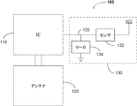
図1は、本発明による近距離通信(NFC)および/またはRFデバイス100(例えばNFCタグ)の例を示す。デバイスは一般に、基板(図示せず)、集積回路(IC)110、ICと連絡するアンテナ120、および、独立してIC110と連絡する1または複数のセンサ130を備える。任意で、NFCデバイス100はまた、独立してIC110と連絡する1または複数の冗長センサも備え得る。この構造および/またはデバイスアーキテクチャはまた、RFIDタグなどの無線周波数(RF)デバイス、ロール読み取り装置、超短波(VHF)デバイス、極超短波(UHF)デバイスなどの高周波(HF)デバイスなどに適用可能である。
FIG. 1 shows an example of near field communication (NFC) and / or RF device 100 (eg, NFC tag) according to the present invention. The device generally comprises a substrate (not shown), an integrated circuit (IC) 110, an
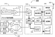
図3は、図1のIC110としての使用に適したIC200の例を示し、それは、1または複数のセンサ210と、センサ210から情報(例えば、信号)を受信する閾値比較部220と、閾値比較部220の出力を受信するパルスドライバ240と、パルスドライバ240からのセンサデータを格納するためのメモリ260と、メモリ260からデータを読み取るための1または複数のビット線(BL)272と、ビット線上の信号をデジタル信号へ変換する1または複数の検知増幅部(SA)274と、検知増幅部274からのデータを一時的に格納するための1または複数のラッチ276と、デバイス(例えば、図1のワイヤレス通信デバイス100)からデータ(識別コードを含む)出力するように構成された送信部(例えば、変調部)290とを含み得る。また、図3の例示的なIC200は、IC200において特定の動作のタイミングを制御するためのタイミング信号(例えばCLK)を提供するように構成されたクロック回路250と、メモリ読み取り動作のタイミングを制御するメモリタイミング制御ブロックまたは回路270とを含む。変調部290はまた、クロック回路270からのタイミング信号(CLK)、または、速度を落とした、もしくは速度を上げた、それらの変形を受信する。例示的なIC200はまた、直流信号(例えばVCC)をIC200内の様々な回路および/または回路ブロックへ提供する、電源ブロックまたは回路280を含む。メモリ260はまた、識別コードを含み得る。識別コードを含むメモリ260の一部は、プリントされ得る。IC200はさらに、受信部(例えば復調部)、1または複数の整流部(例えば、整流ダイオード、1または複数のハーフブリッジもしくはフルブリッジ整流部など)、1または複数の同調もしくは蓄積コンデンサなどを含み得る。変調部290および電源280における端子は、アンテナの端部(例えば、コイル1およびコイル2にて)と接続される。
FIG. 3 shows an example of an
図1に示される本発明の導通センサ130は、センサ材料132およびリーカ(leaker)回路134を含む。図1に示されるように、人は単純に、センサブロック130において高デジタル論理状態に対応する電圧(例えば、上部電源レール[VCC]または高電圧に接続される他の回路素子)にセンサ132を接続し得、ならびにセンサ材料132がIC110に高電圧を電気的に接続しない場合、論理低状態にIC110に対する入力ノード135を駆動する(弱)プルダウンまたはリーカ回路134にセンサ132を接続し得る。プルダウンまたはリーカ回路134は、反対の端子でグランド電圧に接続されている、抵抗器、または抵抗配線トランジスタであり得る。そのような設計においては、メモリビットは必要なく、任意で閾値比較部も必要ない。しかしながら、メモリ260および閾値比較部220(図3)は、追加センサ、識別コードなどを含む実施形態に役立ち得る。
The
図1に示されるように、本発明のタグにおけるセンサ132は、パッケージまたは容器内部の所与の成分または物質への暴露に基づき、伝導性が大きくなる、または小さくなる材料で満たされているトレース中のオープンスペースであり得、またはそれを表し得る。同様な技術が、アンテナを有効または無効にすべく、特定のワイヤレスタグに対して使用されるが、1つの状態は常に、読み取り不能(すなわち、アンテナが無効にされた場合)という結果となる。センサ材料(例えば、図2の136)をトレースに移動することにより、2またはそれ以上の有効状態を可能にする。いくつかの実施形態において、トランジスタ(例えば、1つのソース/ドレインまたはエミッタ/コレクタ端子でのセンサ出力およびゲートまたはベースでの「センサイネーブル」信号を受信する、あるいは、ダイオード配線され得、ソース/ドレインまたはエミッタ/コレクタ端子と、ゲートまたはベースとの両方にてセンサ信号を受信し得る)は、IC110にセンサからの信号を変調し得る。
As shown in FIG. 1, the
そのような場合におけるセンサ材料136は、電解質(例えば、電解質により吸収される水分または水蒸気に暴露された場合にその伝導性が増大する乾燥ゲル電解質)であり得る。「暴露」状態に対する閾値は、(例えば、トレースの寸法、その伝導性が化学薬品への暴露の関数として変化する材料の比率、リーカ回路134を横切る電流などを用いて)経験的に決定され得る。いくつかの実施形態において、センサ材料136のコンダクタンスは、水、一酸化炭素などの特定の気体または化学薬品に対して非線形に変化する。NFCまたは他のワイヤレスタグの上/中にあるセンサ材料136は、物品の環境化学物質への「暴露/非暴露」状態を決定すべく、外部環境に暴露される必要がある。環境化学物質が密封された物品内部にも含まれる化学物質であり、化学物質の濃度が物品を取り巻く環境にて自然に見つけられるものよりも大きい場合であって、センサ材料136のコンダクタンスが変化する場合に、人は、センサ材料136のコンダクタンスの変化が、物品を開封したか、あるいは封を切ることににより引き起こされたと結論づけ得る。
The
図2に示されるように、コンダクタンスなどの材料パラメータが少なくとも1つの環境条件(例えば、湿度、温度、化学物質(例えば、気体または液体))の有無に依存するトランジスタ138などの非線形素子はまた、IC110に入力される信号の値を制御するか、またはそれに影響を及ぼすようにセンサ132において使用され得る。様々な例において、センサ132は、非線形トランジスタ(その閾値電圧または伝導性が、化学物質の吸収によって(例えば、それのゲート材料において)変化する)、化学センサ(その抵抗が化学物質の吸収によって変化する)、膜センサまたは微小電気機械システム(MEMS)ベースセンサなどを含み得る。
As shown in FIG. 2, nonlinear elements such as
その閾値電圧または伝導性が、化学物質の吸収によって変化する非線形トランジスタの例は、湿潤状態と比較して乾燥状態において大きな信号スイングに導くゲートに電解質を有するトランジスタである。ゲートがそのような電解質を含む場合、フィールドの大部分または実質的に全ては、(乾燥状態下で誘電体として機能する)電解質上にあり、従って、ゲート中のそのような電解質を含むn−TFTは、たとえ「オン」状態に対応する電圧がゲートに印加された場合でも、「オフ」状態にある。湿潤状態下では、電解質が伝導し、フィールドがゲート誘電体上に存在し、n−TFTは、「オン」電圧の印加によってオンとなる。1つの例において、(例えば、バッテリ用途に適する)乾燥リチウム高分子電解質が、そのようなトランジスタのゲートとして(例えば、ロールツーロール[R2R]対応のプリント方法を用いて)プリントされ得る。センサ132またはセンサ材料136は、液体(例えば、水)を含む容器のキャップ、栓、コルク栓または他のシールの近くに配置され、シールが切られた後、電解質が液体(例えば、水分または水蒸気)を吸収することとなる。1つの実施形態において、容器の開封は、少量の液体(例えば、電解質のコンダクタンス状態を変化するのに十分な量)をセンサ132またはセンサ材料136に流し込むまたは向けるように設計され得る。センサ132またはセンサ材料136は、そのコンダクタンス状態または値(例えば、その抵抗率)を変化させるのに十分な液体を吸収した場合、トランジスタ138は伝導する(少なくとも、伝導し始める)こととなり、センサ132からの出力信号の状態または値は変化するだろう。ゲートの組成、形状および寸法は、トランジスタのオン/オフ切り替えに対して最適化され得る。代替的な実施形態において、リチウムは、亜鉛イオンで取り替えられ得、および/または電解質は、バッテリ用途に適する別の電解質であり得る(例えば、参照によって関連部分が本明細書に組み込まれた2012年3月22日に公開された国際公開番号WO 2012/037171および/または米国特許出願公開第2013/0280579号を参照)。
An example of a non-linear transistor whose threshold voltage or conductivity varies with chemical absorption is a transistor with an electrolyte at the gate that leads to a large signal swing in the dry state compared to the wet state. If the gate includes such an electrolyte, most or substantially all of the field is on the electrolyte (functioning as a dielectric under dry conditions), and thus n − including such an electrolyte in the gate. The TFT is in the “off” state even if a voltage corresponding to the “on” state is applied to the gate. Under wet conditions, the electrolyte conducts, the field is on the gate dielectric, and the n-TFT is turned on by applying an “on” voltage. In one example, a dry lithium polymer electrolyte (eg, suitable for battery applications) can be printed as the gate of such a transistor (eg, using a roll-to-roll [R2R] compatible printing method). The
その閾値電圧または伝導性が化学物質の吸収によって変化するトランジスタの別の例は、ISFET(イオン選択電界効果トランジスタ)である。その抵抗が化学物質の吸収によって変化する化学センサの例は、ナノワイヤ、カーボンナノチューブ、ならびに、水蒸気感応性のハイドロゲルおよび/または乾燥ゲル、および/または分析物検知蛍光体またはエレクトロホア(例えば、アルコール検知蛍光体)を含む物理マトリックスを含む。その抵抗またはコンダクタンスが化学物質の吸収によって変化する化学センサより具体的な例は、
・ゾルゲル膜中の分析物検知蛍光体、
・抵抗ガスセンサおよびケミレジスタ、
・そのコンダクタンス状態が閾値濃度を超えるガスの存在によって変化し、かつ1または複数の半導体を含み得る、例えば、電界効果デバイス(FED)イオン半導体、FEDガス半導体およびショットキーダイオードなどの半導体およびFEDデバイス、
・例えば、金属、炭素、高分子(例えば、乾燥リチウム)および無機ナノファイバなどのナノ材料、および、
磁気または半導電性ナノ材料、
を含む。
Another example of a transistor whose threshold voltage or conductivity is changed by chemical absorption is an ISFET (ion selective field effect transistor). Examples of chemical sensors whose resistance varies with chemical absorption include nanowires, carbon nanotubes, and water vapor sensitive hydrogels and / or dry gels, and / or analyte sensing phosphors or electrophores (eg, alcohols) A physical matrix containing the detection phosphor). A more specific example of a chemical sensor whose resistance or conductance changes by absorption of chemicals is
-Analyte detection phosphor in sol-gel film,
・ Resistance gas sensor and chemi-register,
Semiconductors and FED devices, such as field effect devices (FED) ionic semiconductors, FED gas semiconductors and Schottky diodes, whose conductance states change with the presence of a gas above a threshold concentration and may include one or more semiconductor ,
-Nanomaterials such as, for example, metals, carbon, polymers (eg dry lithium) and inorganic nanofibers, and
Magnetic or semiconductive nanomaterials,
including.
本発明で使用する、特に有用な電解質は、高分子電解質(すなわち、溶媒和ポリマーマトリックスにおいて解離される塩を含む電解質)を含む。ポリエチレンオキサイド(PEO)は、特にプロトンおよび他の小さなカチオンに対して良好なイオン導体であり、この理由により、高分子電解質においてしばしば使用される。ポリマーは、イオンを伝導または運搬することができるが、それ自体は伝導性がなく、それで塩の形をしたイオン(例えば、過塩素酸リチウム(LiClO4))が通常、加えられる。しかしながら、いくつかの電解質材料は、吸湿性(例えば、PEO)であり得、それにより吸収性電解質材料により吸収される周囲からの水分が、(例えば、H3O+およびOH−イオンへ)解離して、(イオン)伝導性に寄与し得る。吸収された水はまた、高分子電解質のイオン移動性、従ってイオン伝導性に影響を及ぼし得る。 Particularly useful electrolytes for use in the present invention include polyelectrolytes (ie, electrolytes containing salts that are dissociated in a solvated polymer matrix). Polyethylene oxide (PEO) is a good ionic conductor, especially for protons and other small cations, and for this reason is often used in polyelectrolytes. Polymers can conduct or carry ions, but are not themselves conductive, so ions in the form of salts (eg, lithium perchlorate (LiClO 4 )) are usually added. However, some electrolyte materials can be hygroscopic (eg, PEO) so that moisture from the surroundings absorbed by the absorbing electrolyte material can be dissociated (eg, to H 3 O + and OH − ions). Thus, it can contribute to (ion) conductivity. Absorbed water can also affect the ionic mobility and thus ionic conductivity of the polyelectrolyte.
本発明において使用に適する他の電解質は、他の高分子電解質を含む。高分子電解質は、繰り返し単位のイオン基を有する高分子または疑似高分子材料であり、このことはイオンの1つが高分子鎖に結合され(すなわち、可動ではなく)、カウンタイオンは自由に動ける(すなわち、可動である)ことを意味する。高分子電解質は、高分子カチオンおよび高分子アニオンを含み、それらにおいて、可動イオンはそれぞれ、アニオン(−)またはカチオン(+)である。これらのタイプの材料は、通常、吸湿性である。通常、それらは、解離すべく可動イオンの移動性を可能にする水または別の溶媒を必要とする。その結果、それらは、湿気または水分検知用途で使用する良い候補である。 Other electrolytes suitable for use in the present invention include other polyelectrolytes. A polyelectrolyte is a polymer or pseudo-polymeric material having an ionic group of repeating units, which means that one of the ions is bound to the polymer chain (ie not mobile) and the counter ions are free to move ( That is, it is movable). The polyelectrolyte includes a polymeric cation and a polymeric anion, in which the mobile ions are anions (−) or cations (+), respectively. These types of materials are typically hygroscopic. Usually they require water or another solvent that allows the mobility of mobile ions to dissociate. As a result, they are good candidates for use in moisture or moisture sensing applications.
高分子電解質が乾燥した場合、それらはほとんど可動性のないイオン(低移動性を有する場合もあり得る)を含む。材料の(イオン)抵抗は、比較的高い。含水量が増加した場合、より多くのイオンが可動状態になり、これらのイオンの移動性も通常増大する。言い換えれば、イオン伝導性は、増加する。他方では、高分子電解質は、それが乾燥している場合、しばしば伝導性がある。しかしながら、可動電荷キャリア(イオン)の数およびイオンの移動性が含水量の増大と共に潜在的に増大し得、従って水分吸収によってイオン伝導性の増大をももたらす。イオン伝導性の変化は、以下に説明されるように、様々な方法にて使用され得る。 [ブロッキング電極を有するコンデンサ] When the polyelectrolytes are dried, they contain ions that have little mobility (which may have low mobility). The (ion) resistance of the material is relatively high. As the water content increases, more ions become mobile and the mobility of these ions usually increases. In other words, ionic conductivity increases. On the other hand, the polyelectrolyte is often conductive when it is dry. However, the number of mobile charge carriers (ions) and ion mobility can potentially increase with increasing water content, thus also leading to increased ionic conductivity due to moisture absorption. The change in ionic conductivity can be used in a variety of ways, as described below. [Capacitor with blocking electrode]
高分子電解質は、2つのブロッキング電極間に挟まれ、電気化学反応が発生するのを防止するように構成される(すなわち、ファラデー反応は無視してよい、または可能ではない)、コンデンサ構造における絶縁層として使用され得る。乾燥した場合、高分子電解質は主として、層の厚さに比例したキャパシタンスを有する通常の無イオンの誘電体として作用するだろう。従って、電解質にわたって印加される電位は、電解質層内部に大体、均一な電場を生成するであろう。しかしながら、湿った場合、イオンは再分布し、電極における補償電荷と共に、高分子電解質電極の境界に電気的二重層を形成する。印加電位の大部分は、境界でのこれらの比較的薄い二重層にわたって降下するだろう。その結果、キャパシタンスは、非常に高くなり、実質的に厚さ独立となるであろう。キャパシタンスの変化は、数桁の大きさまで高くなり得る。電解質層のイオン伝導性は、デバイスにわたって電圧を印加または変化した後、コンデンサがどのくらい速く充電するであろうかに影響を及ぼす。イオン伝導性がより高くなるほど、コンデンサはより速く(完全に)充電された状態になる。電解質は、デバイスにわたり電圧を印加した直後に通常の誘電体として作用する。すなわち、電極上の電荷が変化し、電場が電解質内部に誘導される。次に、電場はイオンを再分布させ、結局は、電解質電極の境界にて電気的二重層を構築することにより電極をさらに充電する。このイオン緩和が起こった後、電場は境界にて高いが、電荷中性の電解質バルクにおいて比較的小さい。従って、コンデンサの動作は、印加電圧の周波数に依存する。コンデンサは、高周波数にて低キャパシタンスを有する誘電体コンデンサとして、および低周波数にて高キャパシタンスを有する電解質コンデンサとして動作する。電解質のイオン伝導性が、これらの2つの状態間の移行が起こる周波数範囲を決定する。従って、電解質中の含水量は、コンデンサの周波数応答に影響を及ぼし得る。 [電気化学的にアクティブな電極を有するコンデンサ] The polyelectrolyte is sandwiched between two blocking electrodes and is configured to prevent an electrochemical reaction from occurring (ie, the Faraday reaction is negligible or not possible), insulation in the capacitor structure Can be used as a layer. When dried, the polyelectrolyte will act primarily as a normal non-ionic dielectric with a capacitance proportional to the layer thickness. Thus, the potential applied across the electrolyte will generate a roughly uniform electric field within the electrolyte layer. However, when wet, the ions redistribute and, together with the compensating charge at the electrode, form an electrical double layer at the boundary of the polyelectrolyte electrode. Most of the applied potential will fall across these relatively thin bilayers at the boundary. As a result, the capacitance will be very high and will be substantially thickness independent. The change in capacitance can be as high as several orders of magnitude. The ionic conductivity of the electrolyte layer affects how fast the capacitor will charge after applying or changing voltage across the device. The higher the ionic conductivity, the faster (fully) the capacitor is charged. The electrolyte acts as a normal dielectric immediately after applying a voltage across the device. That is, the charge on the electrode changes and an electric field is induced inside the electrolyte. The electric field then redistributes the ions, eventually charging the electrode further by building an electrical double layer at the electrolyte electrode boundary. After this ion relaxation occurs, the electric field is high at the boundary, but relatively small in the charge neutral electrolyte bulk. Therefore, the operation of the capacitor depends on the frequency of the applied voltage. The capacitor operates as a dielectric capacitor having a low capacitance at high frequencies and as an electrolyte capacitor having a high capacitance at low frequencies. The ionic conductivity of the electrolyte determines the frequency range in which the transition between these two states occurs. Thus, the water content in the electrolyte can affect the frequency response of the capacitor. [Capacitors with electrochemically active electrodes]
(例えば、解離した水であり得る)電解質中のイオンと電気化学的に反応し得る両側の電極を有するコンデンサ構造において、絶縁層として使用される高分子電解質は、デバイスに少し異なる方式にて動作させるだろう。電解質が乾燥している場合、デバイスは、非常に高いDC抵抗を有する通常のコンデンサとして本質的に動作するであろう。電解質が湿っている、または(液体または蒸気の形態において)十分な水分を吸収している場合、電解質層のキャパシタンスを増大する電気的二重層が形成されるが、電極の境界での電気化学反応は、電解質層のDC抵抗を低減する。そのようなデバイスは、湿度依存の抵抗器として使用され得る。 [トランジスタにおけるゲート絶縁体] In a capacitor structure with electrodes on both sides that can electrochemically react with ions in the electrolyte (which can be dissociated water, for example), the polymer electrolyte used as the insulating layer operates in a slightly different manner in the device Will let you. If the electrolyte is dry, the device will essentially operate as a normal capacitor with a very high DC resistance. If the electrolyte is wet or absorbs sufficient moisture (in liquid or vapor form), an electrical double layer is formed that increases the capacitance of the electrolyte layer, but the electrochemical reaction at the electrode boundary Reduces the DC resistance of the electrolyte layer. Such devices can be used as humidity dependent resistors. [Gate insulators in transistors]
高分子電解質はまた、電界効果トランジスタ、電気化学トランジスタにおけるゲート絶縁体材料として使用され得る。高分子電解質の含水量の関数としてのゲート絶縁体のキャパシタンスの変化は、(所与の電圧にて)ドレイン電流に著しい影響を及ぼす。理想的には、トランジスタは、この構成が動作するのに適した閾値電圧を有する。そのようなデバイスはまた、可変抵抗器として使用され得る。電解質コンデンサについてと同じように、電解質中の含水量は、トランジスタの周波数応答に影響を及ぼし得る。 Polyelectrolytes can also be used as gate insulator materials in field effect transistors, electrochemical transistors. The change in capacitance of the gate insulator as a function of the water content of the polyelectrolyte has a significant effect on the drain current (at a given voltage). Ideally, the transistor has a threshold voltage suitable for this configuration to operate. Such a device can also be used as a variable resistor. As with electrolyte capacitors, the water content in the electrolyte can affect the frequency response of the transistor.
例えば、ポリスチレンスルホン酸(PSSA/PSSH/PSS)、ポリアクリル酸(PAA)、ポリビニルホスホン酸(PVPA)およびそれらのコポリマなどのポリアニオン系の高分子電解質は、良い結果を伴って有機薄膜トランジスタ(OTFT)において使用され得る。そのような高分子電解質は十分吸湿性であり、それらが、低い相対湿度でさえ、高レベルにイオン伝導性(またはキャパシタンス)を保つのに十分な水分を保持することが考えられる。しかしながら、高分子電解質は、特定の状況下で完全に乾いて、イオン伝導性を低減する場合がある。例えば、実験は、(周囲の含気環境とは対照的に)乾燥窒素を用いたエアフロー中に配置された、ポリ(ビニルホスホン酸−アクリル酸)コポリマ(P[VPA−AA])高分子電解質を含むOTFTが、周囲の含気環境における同じOTFTと比較して、ドレイン電流が劇的に低下する結果となることを証明した。 For example, polyanionic polymer electrolytes such as polystyrene sulfonic acid (PSSA / PSSH / PSS), polyacrylic acid (PAA), polyvinyl phosphonic acid (PVPA) and their copolymers have organic thin film transistors (OTFTs) with good results. Can be used. Such polyelectrolytes are sufficiently hygroscopic and it is believed that they retain sufficient moisture to maintain high levels of ionic conductivity (or capacitance) even at low relative humidity. However, polyelectrolytes may dry completely under certain circumstances, reducing ionic conductivity. For example, experiments have shown that a poly (vinyl phosphonic acid-acrylic acid) copolymer (P [VPA-AA]) polyelectrolyte placed in an air flow with dry nitrogen (as opposed to the ambient air atmosphere) It has been demonstrated that OTFTs containing can result in a dramatic reduction in drain current compared to the same OTFT in the surrounding aerated environment.
図3を参照すると、NFCおよび/またはRFIDタグ200内のメモリ260は、固定数のビットを含み得る。いくつかの実装において、NFCおよび/またはRFIDタグ200内のメモリ260は、mを正の整数、nを少なくとも3の整数として、m×2nビット(例えば、24、32、48、64、128、256、または、それより多くのビット)を含み得る。いくつかのビットは、フォーマットの識別、および、データ完全性(CRC)のチェックのため、オーバーヘッド(非ペイロード)データに割り当てられる。デバイス200のペイロードは、残りのビットを消費する。例えば、ペイロードは最大で(m−p)×2nビットであり得る。ここで、pは、mより小さい正の整数である(例えば、m×2n=128ビットの場合は96ビットであり、m×2n=256ビットの場合は最大224ビットである)。
Referring to FIG. 3, the
NFCおよび/またはRFIDタグ200のペイロードは、可変量の固定ROMビット(常にではないが、一般的に、固有の識別番号として使用される)に割り当てられ得る。NFCおよび/またはRFIDタグ200の製造において、プリントの方法が使用される場合、ROMビットは永久的に符号化され、電気的に修正できない。固定ROMビットとして割り当てられない任意のペイロードビットは、動的センサビットとして割り当てられ得る。これらのセンサビットは、検知された入力に基づいて、値を変更し得る。ROMおよびセンサビットの間の異なる分割または割り当ては一般的に、NFCおよび/またはRFIDタグメモリ260の最初の2nビット(または、qをnより小さい正の整数として、2n−qビット(例えば、m×2n=128または256の場合、16ビット))内にある非ペイロードまたは「オーバーヘッド」ビットの一部である、データフォーマットビットによって示される。
The payload of the NFC and / or
NFCおよび/またはRFIDタグ200ならびにメモリ260においてどのようにして検知が実装されるかについての1つの例は、周囲環境が密封パッケージ中に化学物質を含むが、これが密封パッケージを開封時または切った時に周囲環境へと解放され得る(例えば、水分、アルコールなどの)化学物質を含む場合に検出する化学センサ210を伴う。そのようなイベント時には、センサ210は、化学物質の存在を反映すべく状態を変化する。ROM IDビットは変化しないが、データ完全性ビット(例えば、CRC)は、センサ210の状態を反映するように更新され得る。これは、保護容器が開封された、あるいは損なわれたことを読み取り装置(例えば、NFCスマートフォンなど)に示す。
One example of how sensing is implemented in the NFC and / or
本出願において、導通検知は一般的に、容器が開封されたか、または損なわれたか、あるいは未開封状態(例えば、工場で密封された状態)を維持しているかを検知または判定する能力および/または機能を指す。1つの実施形態において、導通検知は、図1に示されるように、1または複数のセンサ130を使用して実装される。図1に例示されるように、本発明のNFC/RFタグ100は、IC110、アンテナ120およびセンサ130の3つの部分を含み得る。IC110およびアンテナ120を含むタグの部分は、保護製品および/またはパッケージ/ラベル上のどこかにあり得る。センサ130は、IC110およびアンテナ120と、保護製品および/またはパッケージラベルの同一部分上にあるが、センサ130は通常、パッケージまたは容器の密封および/または開封部位に比較的近い。
In this application, continuity detection generally has the ability to detect or determine whether a container has been opened or damaged, or remains unopened (eg, sealed at the factory) and / or Refers to function. In one embodiment, continuity detection is implemented using one or
例えば、特定の医薬品において、容器、ボトルまたはジャーは、液体または蒸気形態の薬品を含み得る。センサ132を含むタグの一部は、容器、ボトルまたはジャー上のIC110から安全キャップまたはシールの方に延在し、それにより安全キャップが除去された、またはシールが破損された場合、液体または蒸気の存在を検知する位置にある。キャップが除去された場合、センサ132は直近の環境にある液体または蒸気の存在を検出し、導通センサ130および/またはIC110は、容器についての開封状態を検知または判定する。
For example, in certain pharmaceuticals, a container, bottle or jar may contain a drug in liquid or vapor form. The portion of the tag that includes the
ブリスターパックにおいては、個別のセンサは、センサおよびICがどの区画が開封されたか(および、いくつかの実施形態において、開封された各区画はいつ開封されたか)を判定できるように、(通常は開封されない、および、個別の区画を密封するホイルまたはプラスチックフィルムが通常容易に除去されない、ブリスターパックの領域内にあり得る)ICから、それぞれの区画の各々の方に延在し得る。箱入りの製品において、NFC/RFタグを含むラベルまたはテープは、箱を閉じて密封するように合わされてテープ付けされる2つのフラップ間の境界近く、または蓋およびトレイ間の境界近くに配置され得、それによりセンサは境界の近くにある。箱を開封することにより、センサをその中の化学物質を暴露し、容器のための異なる導通状態が検出され得る。同様のアプローチおよび/または技術は、多くの異なるタイプの製品容器(例えば、ジュエリー、腕時計などのためのヒンジ式の蓋が付いた箱と、アルコール用ボトルと、タバコパッケージと、紐、フィラメント、または他の頑丈な材料の条片などを引くことで開封できる、翌日配達封筒などの出荷パッケージ)に適用され得る。 In blister packs, individual sensors can (usually determine which compartments were opened by the sensor and IC (and in each embodiment when each opened compartment was opened)). It can extend from the IC (which can be in the area of the blister pack, which is not opened and the foil or plastic film that seals the individual compartments is usually not easily removed) towards each of the respective compartments. In a boxed product, a label or tape containing an NFC / RF tag can be placed near the boundary between two flaps that are taped together to close and seal the box, or near the boundary between the lid and tray. , So that the sensor is near the boundary. By opening the box, the sensor can be exposed to chemicals therein and different conduction states for the container can be detected. Similar approaches and / or techniques are available for many different types of product containers (e.g., boxes with hinged lids for jewelry, watches, etc., alcohol bottles, tobacco packages, strings, filaments, or It can be applied to shipping packages such as next-day delivery envelopes that can be opened by pulling strips of other sturdy materials.
本発明のNFC/RFタグは、1または複数の追加および/または冗長センサ(すなわち、導通センサに加えて)を含み得る。冗長センサは、導通センサと共に「AND」型関数(例えば、ICおよびセンサは、センサおよび冗長センサの全てが状態を変化した場合にのみ、容器が開封されたことを検知する)において、または、センサと共に「OR」型関数(例えば、ICおよびセンサは、センサおよび冗長センサのいずれかが状態を変化した場合に、容器が開封されたことを検知する)において、使用され得る。代替的に、センサおよび冗長センサは、センサおよび冗長センサの1または複数が状態を変化させた場合に、およびセンサおよび冗長センサの1または複数が状態を変化させなかった場合に、1または複数の「部分的に開封された」導通状態を提供することができる。当業者は、そのような機能および/または能力のためのロジックおよびアプリケーションを容易に導き出すことができ、冗長センサおよび/または追加センサ(追加センサが、導通センサによって検知される化学物質以外の化学物質を検知するための湿度センサ、温度センサ、電磁界センサもしくは化学センサである、またはそれを含む場合)は、導通センサと同じ様式および/または全体構造にて製造され得る。 The NFC / RF tag of the present invention may include one or more additional and / or redundant sensors (ie, in addition to a continuity sensor). Redundant sensor in conjunction with a continuity sensor in an “AND” type function (eg, IC and sensor detect that a container has been opened only when all of the sensor and redundant sensor change state) or sensor In conjunction with "OR" type functions (eg, ICs and sensors detect that a container has been opened when either the sensor or the redundant sensor changes state). Alternatively, the sensor and redundant sensor may be one or more when one or more of the sensor and redundant sensor has changed state and when one or more of the sensor and redundant sensor has not changed state. A “partially opened” conducting state can be provided. Those skilled in the art can easily derive the logic and applications for such functions and / or capabilities, and use redundant sensors and / or additional sensors (a chemical other than the chemical that is detected by the continuity sensor). The humidity sensor, temperature sensor, electromagnetic field sensor or chemical sensor for detecting (if included) may be manufactured in the same manner and / or overall structure as the continuity sensor.
当然、本発明のNFC/RFタグにおけるIC110は、導通センサ130に加えて、1または複数のセンサを含み得る。例えば、IC110はさらに、1または複数の温度センサ、(例えば、導通センサから独立したパッケージ環境の湿度レベルをテストするための)湿度センサ、電磁場センサ、電流/電圧/電力センサ、光センサ、または他の化学センサ(例えば、酸素、一酸化炭素、二酸化炭素、窒素酸化物、二酸化硫黄および/または三酸化硫黄、オゾン、または、1または複数の毒物などのための)を含み得る。また、本発明のIC110は、当技術分野において公知であるように、図3のクロック回路250および1または複数の(リアルタイムクロックの基礎であり得る)カウンタおよび除算部などを含む、(例えば、経過時間を計数または判定するように構成されている)1または複数の時間センサを含み得る。任意の外部検知機構からのリード線は、アンテナ120および導通センサ130のための端子とは別の端子で、IC110に接続される必要がある。そのようなセンサは通常、アンテナ120およびIC110とパッケージまたは容器の同一部分上にある。
Of course, the
このソリューションにおいて、NFCタグがその上/その中に内蔵されている製品が未開封状態か、開封状態かに関係なく、NFC機能(すなわち、ワイヤレス読み取り機能)は、常に利用可能である。これは、容器が開封された後で、アンテナが永久的に破損され、従って、タグが読み取り不能となる、従来の実装と対照的である。この新しい実装において、保護製品の開封時、アンテナ線は無傷であり、導通センサ線が状態を変化するので、NFCデータは読み取り装置(スマートフォン、USB読み取り装置など)に対し、そのNFCおよび/またはRFIDタグの固有のID番号(モバイルマーケティング、顧客ロイヤルティ、および値引き/クロスセルの提示から、サプライチェーントラッキング、政府のための税金トラッキング、例えば、ロット番号や製造日など特定の製品製造情報を提供することまで、全てのものに使用できる)だけでなく、保護製品が工場密封/未開封状態(従って、純正品を含む)か、または、開封されたか、または損なわれた(従って、その状態で消費者に届く場合、内容が疑わしい)かを示すだろう。従って、いくつかの実施形態において、容器の開封による、アンテナ(および、任意でIC)に対する意図しない損傷のリスクを低減または最小化するべく、容器の2つの部分の間の境界から十分離れた距離にアンテナ(および、任意でIC)を配置することは有益であり得る。 In this solution, the NFC function (ie, wireless reading function) is always available, regardless of whether the product with the NFC tag on / in it is unopened or unopened. This is in contrast to conventional implementations where the antenna is permanently damaged after the container is opened, thus making the tag unreadable. In this new implementation, when the protection product is opened, the antenna line is intact and the continuity sensor line changes state, so NFC data is sent to the reader (smartphone, USB reader, etc.) and its NFC and / or RFID The unique ID number of the tag (mobile marketing, customer loyalty, discount / cross-sell presentation, supply chain tracking, government tax tracking, eg providing specific product manufacturing information such as lot number and date of manufacture) Not only can be used for everything), but also the protection product is factory sealed / unopened (thus including genuine products), or has been opened or damaged (and therefore consumers in that state) If it arrives, it will indicate whether the content is suspicious). Thus, in some embodiments, a distance sufficiently away from the boundary between the two parts of the container to reduce or minimize the risk of unintentional damage to the antenna (and optionally the IC) due to the opening of the container. It may be beneficial to place an antenna (and optionally an IC) on the board.
開封の前と開封の後の両方において、タグを読み取る能力を維持する(および、容器が開封されたかどうか読み取る特徴を追加する)ことによって、製品が開封された後に、ユーザとのNFCベースのインタラクションを継続することが可能となる。例えば、医薬品、化粧品、特定のアルコール飲料、さらには、オリーブオイルなどの食品は、開封後、数日間、数週間、数か月間、または、さらには数年間使用され得る。この時間の間にNFCおよび/またはRFIDタグの機能を維持することで、消費者は、NFCタグを有する特定の製品に関して、製造業者と連絡できる。 NFC-based interaction with the user after the product has been opened by maintaining the ability to read the tag both before opening and after opening (and adding a feature that reads whether the container has been opened) Can be continued. For example, pharmaceuticals, cosmetics, certain alcoholic beverages, and even foods such as olive oil can be used for several days, weeks, months, or even years after opening. By maintaining the functionality of the NFC and / or RFID tag during this time, the consumer can contact the manufacturer regarding the specific product with the NFC tag.
NFCおよび/またはRFIDタグを読み取る適用例は一般的に、読み取られるIDに関する情報を収集するクラウドサーバに接続される。これは、分析のためにデータを記録すること、ならびに、消費者のスマートフォンまたは他のNFCおよび/またはRF対応デバイスに対して、適切なエクスペリエンスを提供、および/または、正確な情報を提供することを目的としている。「開封」状態を示すIDが最初に読み取られ、クラウドシステムによって処理されるとき、そのIDが再度、仮に「未開封」状態で読み取られる場合、自動的にアラートを発生させるだろう(場合によっては、調査を行わせる)。これは、システム全体の完全性を確実にする上で役立つ。この機能および/または使用法は、容器が開封されるときにNFCおよび/またはRFアンテナが破壊される従来の方法では不可能である。 Applications that read NFC and / or RFID tags are typically connected to a cloud server that collects information about the ID being read. This is to record data for analysis and to provide an appropriate experience and / or provide accurate information to the consumer's smartphone or other NFC and / or RF-enabled device It is an object. When an ID indicating an “open” state is first read and processed by the cloud system, it will automatically generate an alert if it is read again in an “unopened” state (in some cases , Make an investigation). This helps to ensure the integrity of the entire system. This function and / or usage is not possible with conventional methods where the NFC and / or RF antenna is destroyed when the container is opened.
加えて、保護製品の開封時、NFCおよび/またはRFIDタグのデータの状態が変化することとなるので、NFCおよび/またはRFデバイス(例えば読み取り装置)および/またはクラウドシステムは、この状態変化を認識でき、開封後、保護製品またはパッケージに取り付けられたNFCおよび/またはRFIDタグとユーザがインタラクトするときに、差別化されたエクスペリエンスを提供できる。例えば、未開封製品は、(例えば、小売環境における)製品の評価および購入に関連する、消費者および/またはユーザのエクスペリエンスを発生させ得て、開封された製品は、(例えば、食品の場合はレシピを、および/または、医薬品の場合には有効期限や使用上の特別の指示を提供することなどによって)製品の適切な使用方法に関する情報、および/または、関連製品をすぐに注文する、もしくは、同一製品を再注文するなどの機会を発生させ得る。 In addition, when the protection product is opened, the data state of the NFC and / or RFID tag will change, so the NFC and / or RF device (eg, reader) and / or cloud system will recognize this state change. And can provide a differentiated experience when the user interacts with the NFC and / or RFID tag attached to the protective product or package after opening. For example, an unopened product may generate a consumer and / or user experience related to product evaluation and purchase (eg, in a retail environment), and an unopened product (eg, in the case of food) Ordering information on the proper use of the product (e.g. by providing a recipe and / or in the case of medicines an expiration date or special instructions on use) and / or related products immediately, or , An opportunity such as reordering the same product may be generated.
導通(保護)検知線の状態の変化によって、NFCデータの多くの、または、全てのビットが変化させられる適用例には、より複雑な実装が使用され得る。これは、シフト、XOR、または、他の公知の関数など、予想可能な方式で行われ得るか、または、予測不可能な方式(ブランドオーナーによって維持されるプライベートクラウドデータベース内のみにある「未開封」IDにリンクされていて、一般人がアクセスできない、完全に異なるランダムな「開封」IDで、ランダムなIDを完全に置き換えるなど)で行われ得る。これらの機能は、タグのコピーを、より一層難しくする。当然、NFCおよび/またはRFIDタグデータストリーム内のCRC完全性は維持される必要がある。 More complex implementations can be used in applications where many or all bits of NFC data are changed by changing the state of the continuity (protection) sense line. This can be done in a predictable manner, such as shift, XOR, or other known functions, or in an unpredictable manner ("unopened" which is only in the private cloud database maintained by the brand owner ”Linked to the ID and inaccessible to the general public, or completely replacing the random ID with a completely different random“ open ”ID). These functions make tag copying even more difficult. Of course, CRC integrity within the NFC and / or RFID tag data stream needs to be maintained.
この実装の、特に高セキュリティのバージョンは、完全にランダムなIDのペアを伴い、1つは「開封」を表し、1つは「未開封」を表し、ブランドオーナー、または、保護システムの管理者によって管理されるデータベース内のみで知られている関連付けを有する。「開封」値は「未開封」値のみから絶対に判定できず、「未開封」値は「開封」値のみから絶対に判定できないので、このシステムは、特に有益である。開封の前および後に、NFCフォンおよび関連する適用例によって読み取られるとき、保護製品が現在、「開封」状態か、「未開封」状態か記録するべく、クラウドデータベースによって、異なるIDが復号される。有効な「開封」IDのセットは、単純に「未開封」の在庫を体系的に読み取ることによってスキミングできないので、これは最初、IDの複製を非常に困難にする。スキャンを行うとき、消費者は、製品の妥当性に関するいくつかの情報を受信することを覚えておくべきである。例えば、実地において、シリアル番号0210番を有する製品があるとする。未開封IDは、ID−Aであり、開封IDは、ID−Bである。クラウドシステムがシステムからID−Aを受信し、その後、同一のスマートフォンからID−Bを受信した場合、同一ユーザが商品0210番を開封したことを推測できる。しかしながら、システムが、ID−Bの読み取り後に、ID−Aの読み取りを受信した場合、何か異常がある。なぜなら、これらのIDは、商品0210番のみに割り当てられたものであり、センサを破損してNFCおよび/またはRFIDタグを「開封」IDに変えることによって、商品が永久的に物理的に変化した後で、「未開封」IDが読み取られることは不可能だからである。このことは、IDがコピーされたことを意味し得て、(必要に応じて)ユーザ/ブランドオーナー/流通業者/小売業者に対してアラートを送ることができ、詐欺および他のサプライチェーンの混乱を隔離するべく、詳細が追跡される。そのような一般的な詐欺検出の概念は、クレジットカード詐欺を検出するためのルール(例えば、カードがフロリダで読み取られ、数分後、ロンドンで読み取られると、詐欺アラートがトリガされる)を策定するときに使用される概念と同様であり得る。 A particularly high-security version of this implementation involves a completely random ID pair, one representing “open”, one representing “unopened” and the brand owner or administrator of the protection system Has a known association only in the database managed by. This system is particularly useful because the “open” value cannot be determined from the “unopened” value alone, and the “unopened” value cannot be determined from the “open” value alone. Different IDs are decrypted by the cloud database to record whether the protection product is currently in the “open” or “unopened” state when read by the NFC phone and related applications before and after opening. This initially makes it very difficult to duplicate IDs, since a set of valid “open” IDs cannot be skimmed simply by systematically reading “unopened” inventory. When doing a scan, the consumer should remember to receive some information about the validity of the product. For example, it is assumed that there is a product having serial number 0210 in practice. The unopened ID is ID-A, and the unsealed ID is ID-B. When the cloud system receives ID-A from the system and then receives ID-B from the same smartphone, it can be inferred that the same user has opened item 0210. However, if the system receives ID-A reading after reading ID-B, something is wrong. Because these IDs are only assigned to product number 0210, the product has been permanently changed physically by damaging the sensor and changing the NFC and / or RFID tag to an “open” ID. This is because the “unopened” ID cannot be read later. This can mean that the ID has been copied and can send alerts to users / brand owners / distributors / retailers (if necessary), fraud and other supply chain disruptions Details are tracked to isolate. Such a common fraud detection concept formulates rules for detecting credit card fraud (for example, fraud alerts are triggered when a card is read in Florida and after a few minutes in London) It can be similar to the concept used when doing.
さらにまた、2つの完全にランダムなIDの使用は、悪意のある者が、システムを脆弱化するべく、IDを「開封」としてトリガ(trigger)することを試みる状況を克服できる。「開封」IDが「未開封」IDから容易に取得できないとき、そのような状況は不可能である。これによって、システム内において、詐欺に対する対抗策の他の層を提供する。 Furthermore, the use of two completely random IDs can overcome the situation where a malicious party attempts to trigger the ID as “open” to weaken the system. Such a situation is not possible when the “open” ID cannot be easily obtained from the “unopened” ID. This provides another layer of fraud countermeasures within the system.
セキュリティのさらなる層のために、NFCラベルは、改ざん明示機能のある固着剤および紙と組み合わせることができる。このように、消費者、小売業者、流通業者、またはブランド代表者に対し、ラベルが改ざんされたかどうか、視覚的に示される。 For an additional layer of security, NFC labels can be combined with stickers and paper with tampering capabilities. In this way, it is visually indicated to the consumer, retailer, distributor, or brand representative whether the label has been tampered with.
アンテナ120は(例えば、これらに限定されないが、銀ペーストまたは銀インクからの銀などのプリントされた導体を使用して)プリントでき、または、(例えば、アルミニウムを、プラスチックフィルムもしくはシートなどの基板上にスパッタもしくは蒸着させ、低分解能(例えば、10〜1,000μmの線幅)のフォトリソグラフィーによるパターニング、および、ウェットエッチングもしくはドライエッチングによる)アルミニウムのエッチングなどの従来の方法を使用して製造できる。導通センサ130からアンテナコイルを電気的に分離すべく、アンテナ120は、基板材料の導通センサ130とは反対側にパターン化され得る。アンテナ120のサイズおよび形状は、NFC読み取りハードウェアの対象周波数である13.56MHzとの適合性を維持しながら、複数のフォームファクタのいずれかに一致し得る。
The
本発明は、特に、RFIDタグが、外部センサ入力を受けること、および、そのようなタグを読み取るように適用されているRFID読み取り装置によって読み取られるときにそれを通信することを行う能力または機能を有する場合、(例えば、高周波[HF]帯域[3−30kHz]、超短波[VHF]帯域[30−300kHz]、極超短波(UHF)帯域[300−3000kHz]における)13.56MHzより高い、または低い周波数で動作するRFIDタグを含む、全てのRFIDタグ(HF/NFC/13.56MHzタグだけでない)へ幅広く適用され得る。 [ワイヤレス通信デバイスを製造する例示的な方法] The present invention particularly has the ability or function to allow an RFID tag to receive external sensor input and communicate it when read by an RFID reader that is adapted to read such a tag. Higher or lower frequency (eg, in high frequency [HF] band [3-30 kHz], ultra high frequency [VHF] band [30-300 kHz], ultra high frequency (UHF) band [300-3000 kHz]) It can be widely applied to all RFID tags (not just HF / NFC / 13.56 MHz tags), including RFID tags that operate at. Exemplary Method for Manufacturing a Wireless Communication Device
本発明はまた、ワイヤレス通信デバイスを製造する方法に関する。この方法は、第1基板上にアンテナを形成する段階と、共通の基板または異なる基板(すなわち、第1基板または第2の異なる基板)上に1または複数の導通センサを形成する工程と、基板上に集積回路(IC)を形成する工程と、(i)アンテナをICの第1セットの端子に、(ii)導通センサをICの第2セットの端子に、電気的に接続する工程とを含む。IC基板は、アンテナおよび/または導通センサが形成される基板(すなわち、第1基板、または、存在する場合、第2基板)と共通であり得る。代替的に、IC基板は、アンテナおよび導通センサの各々が形成される基板と異なり得る(すなわち、アンテナおよびセンサが同一の(例えば、第1の)基板上に形成される場合は第2基板、あるいは、アンテナおよびセンサが異なる基板上に形成される場合は第3の基板)。アンテナは、ワイヤレス信号を受信、および/もしくは、送信、または、ブロードキャストするように構成される。 The invention also relates to a method of manufacturing a wireless communication device. The method includes forming an antenna on a first substrate, forming one or more continuity sensors on a common substrate or different substrates (ie, a first substrate or a second different substrate), and a substrate Forming an integrated circuit (IC) thereon; and (i) electrically connecting the antenna to the first set of terminals of the IC and (ii) electrically connecting the continuity sensor to the second set of terminals of the IC. Including. The IC substrate may be common with the substrate on which the antenna and / or continuity sensor is formed (ie, the first substrate, or the second substrate, if present). Alternatively, the IC substrate may be different from the substrate on which each of the antenna and continuity sensor is formed (ie, the second substrate if the antenna and sensor are formed on the same (eg, first) substrate, Alternatively, a third substrate if the antenna and sensor are formed on different substrates). The antenna is configured to receive and / or transmit or broadcast wireless signals.
様々な実施形態において、ワイヤレス通信デバイスは、近距離または無線周波数通信デバイスを備える。1つの例において、デバイスは、NFCタグなどのNFCデバイスである。 In various embodiments, the wireless communication device comprises a near field or radio frequency communication device. In one example, the device is an NFC device such as an NFC tag.
ワイヤレス通信デバイスを製造する方法のいくつかの実施形態は、複数の導通センサを製造する工程を含み得る。追加的または代替的に、方法はさらに、本明細書に説明されているように、1または複数の冗長導通センサを形成する工程を含み得る。冗長な導通センサは、導通センサと同一の基板上に形成され得る。 Some embodiments of a method of manufacturing a wireless communication device may include manufacturing a plurality of continuity sensors. Additionally or alternatively, the method may further include forming one or more redundant continuity sensors, as described herein. The redundant continuity sensor can be formed on the same substrate as the continuity sensor.
本発明のワイヤレス通信デバイスを製造する方法において、集積回路を形成する工程は、集積回路の1または複数の層をプリントする工程を含み得る。フォトリソグラフィーパターニングプロセスと比較して、プリント工程には、装置の費用が安い、スループットが大きい、廃棄物が少ない(従って、「よりグリーンな」製造プロセス)などの利点を提供し、近距離、RF、およびHFタグなど、トランジスタ数が比較的少ないデバイスに理想的であり得る。従って、いくつかの場合において、方法は、集積回路の複数の層をプリントする工程を含み得る。ワイヤレス通信デバイスの様々な層(および1つの例において、層の全て)をプリントすることにより、ロールツーロール処理などの既存の高速、高スループットの製造プロセスへの製造方法の統合を容易にする。 In the method of manufacturing a wireless communication device of the present invention, forming an integrated circuit may include printing one or more layers of the integrated circuit. Compared to photolithography patterning process, the printing process offers advantages such as low equipment cost, high throughput, low waste (and thus “greener” manufacturing process), short range, RF And may be ideal for devices with relatively few transistors, such as HF tags. Thus, in some cases, the method can include printing multiple layers of the integrated circuit. Printing various layers (and all of the layers in one example) of a wireless communication device facilitates integration of manufacturing methods into existing high speed, high throughput manufacturing processes such as roll-to-roll processing.
代替的に、方法は、1または複数の薄膜処理技術によって集積回路の複数の層を形成する工程を含むプロセスによって集積回路を形成する工程を含み得る。薄膜処理はまた、所有費用が比較的低く、比較的成熟した技術であるので、様々な幅広い潜在的な基板上に製造される、合理的に信頼できるデバイスとなり得る。いくつかの実施形態において、両方のアプローチのうち、最適なアプローチを使用でき、方法は、1または複数の薄膜処理技術、および、集積回路の1または複数の追加の層のプリントによって、集積回路の1または複数の層を形成し得る。 Alternatively, the method may include forming the integrated circuit by a process that includes forming multiple layers of the integrated circuit by one or more thin film processing techniques. Thin film processing can also be a reasonably reliable device manufactured on a wide variety of potential substrates because it is a relatively mature technology with a relatively low cost of ownership. In some embodiments, the best of both approaches can be used, and the method can be achieved by printing one or more thin film processing techniques and printing one or more additional layers of the integrated circuit. One or more layers may be formed.
いくつかの実施形態において、アンテナを形成する工程は、第1基板上に単一金属層を形成する工程、および、単一金属層をエッチングしてアンテナを形成する工程から成り得る。代替的に、アンテナを形成する工程は、アンテナに対応するパターンで、第1基板上に金属インクをプリントする工程を含み得る。いくつかの比較的有利な実施形態において、アンテナは、共通の基板上の単一の共通の金属層から成り、ICは、ICがアンテナの端子間のストラップまたはブリッジとして機能するのを可能にし、従ってアンテナの端子をICに電気的に接続するのを可能にするように、形成または製造される。これにより、単一のパターン化された金属層から成るアンテナの使用を可能にする。 In some embodiments, forming the antenna may comprise forming a single metal layer on the first substrate and etching the single metal layer to form the antenna. Alternatively, forming the antenna may include printing metal ink on the first substrate in a pattern corresponding to the antenna. In some relatively advantageous embodiments, the antenna consists of a single common metal layer on a common substrate, the IC allows the IC to function as a strap or bridge between the terminals of the antenna, It is thus formed or manufactured to allow the antenna terminals to be electrically connected to the IC. This allows the use of an antenna consisting of a single patterned metal layer.
本明細書に説明されるように、タグは通常、集積回路および導通センサを含む。その結果として、集積回路(IC)に導通センサを電気的に接続する工程は、IC上またはその中の端子セットに導通センサを電気的に接続する工程を含む。さらにまた、集積回路はさらに、センサの出力を受信するように構成されている閾値比較部、容器またはパッケージの導通状態に対応する値を格納するように構成されている1または複数のビットを含むメモリ、および/または、本明細書に開示されている他の回路もしくは回路ブロックのいずれかを含み得る。例えば、メモリは、容器またはパッケージのための固有の識別コードを格納するように構成されている複数のビットを含み得る。そのような場合には、メモリを形成する工程は、(例えば、マスクROMと同様に、ハードワイヤードROMを形成すべく)固有の識別コードを格納するように構成されている複数のビットを含む、メモリの少なくとも1つの層をプリントする工程を含み得る。 [1または複数のセンサを有する代替的なワイヤレス通信デバイス] As described herein, a tag typically includes an integrated circuit and a continuity sensor. As a result, electrically connecting a continuity sensor to an integrated circuit (IC) includes electrically connecting the continuity sensor to a set of terminals on or in the IC. Furthermore, the integrated circuit further includes a threshold comparison unit configured to receive the output of the sensor, one or more bits configured to store a value corresponding to the conduction state of the container or package. It may include a memory and / or any of the other circuits or circuit blocks disclosed herein. For example, the memory may include a plurality of bits configured to store a unique identification code for the container or package. In such a case, forming the memory includes a plurality of bits configured to store a unique identification code (eg, to form a hard-wired ROM, similar to a mask ROM). Printing at least one layer of memory may be included. [Alternative wireless communication device with one or more sensors]
図4−図5は、1または複数の導通センサ素子またはセンサアレイ、1または複数のセンサインタフェース回路、およびワイヤレス読み取り装置と通信するための1または複数のアンテナ350、440に結合される集積回路を有するワイヤレス通信デバイス300、400(例えば、NFCまたはRFIDタグ)を示す。いくつかの実施形態において、ワイヤレス通信デバイス300、400はさらに、統合ディスプレイを含み得る。
4-5 illustrate an integrated circuit coupled to one or more continuity sensor elements or sensor arrays, one or more sensor interface circuits, and one or
複数のセンサ素子(またはセンサアレイ)を有するセンサは、複数の化学種、化学種および温度、湿度または明るさ(光)等の1または複数の環境パラメータの検出のために、あるいは同一の化学種の検出のための冗長センサとして使用され得る。適合されたパッシベーション層は、センサの特異性を高めることができる。従って、複数のセンサアレイは、所与の用途に対して要求される場合があるように、同じセンサまたは異なるタイプのセンサの複数のコピーを含み得る。 A sensor having a plurality of sensor elements (or sensor arrays) is used for the detection of one or more environmental parameters such as a plurality of chemical species, chemical species and temperature, humidity or brightness (light), or the same chemical species. Can be used as a redundant sensor for detection of The adapted passivation layer can increase the specificity of the sensor. Thus, multiple sensor arrays may include multiple copies of the same sensor or different types of sensors, as may be required for a given application.
化学物質の吸収によってその性質が変化する追加の化学センサの例は、その中に分散される1または複数の分析物検知蛍光体またはエレクトロホア(例えば、アルコール検知蛍光体)を含む物理マトリックスを有するハイドロゲルおよび/または乾燥ゲルを含むことができる。より具体的には、そのような化学センサの例は、ゾルゲルマトリックスまたは膜中の分析物検知蛍光体、および熱化学センサ(その温度が分析物との反応によって変化する、または、容器内の化学薬品または物質に対して、その温度変化が熱量測定により判定される)を含む。 Examples of additional chemical sensors whose properties change upon absorption of a chemical have a physical matrix that includes one or more analyte sensing phosphors or electrophores (eg, alcohol sensing phosphors) dispersed therein. Hydrogels and / or dry gels can be included. More specifically, examples of such chemical sensors include analyte-sensing phosphors in sol-gel matrices or membranes, and thermochemical sensors (the temperature of which varies depending on the reaction with the analyte or the chemical in the container For chemicals or substances, the temperature change is determined by calorimetry).
様々なタイプの金属特有のシード層を用いて個別のセンサ素子の様々なセクションをプリントし、次に様々なシード層上に様々な金属(例えば、パラジウム、金、銀など)をめっきすることがまた望ましい場合がある。 例えば、このアプローチは、センサ素子の一部にパラジウム電極/センサ素子を提供し、一部に金または銀電極/センサ素子を提供し、本質的にセンサ素子内にマルチセンサアレイを作り出す。これはまた、例えば、化学種の様々な金属との反応または結合と、センサ素子における様々な金属の量または関係性とに依存して固有の電流シグネチャを提供する。 Printing different sections of individual sensor elements using different types of metal-specific seed layers and then plating different metals (eg palladium, gold, silver, etc.) on different seed layers It may also be desirable. For example, this approach provides palladium electrodes / sensor elements for some of the sensor elements and gold or silver electrodes / sensor elements for some, essentially creating a multi-sensor array within the sensor elements. This also provides a unique current signature depending on, for example, the reaction or binding of chemical species with various metals and the amount or relationship of the various metals in the sensor element.
図4に示されるように、センサ312をローカル増幅部314を有するおよび/または他のアナログ信号調整回路(例えば、温度補償、ドリフト、オフセットなど)と統合することで、例えば、信号対雑音比を改善することによりセンサ性能を向上し得、より低いレートの偽陽性結果をもたらし得る。図4の較正ブロックに示されるようにローカル比較部328に結合される複数のセンサ素子312および322を使用することにより、個別の導通センサ310は、従来のロット較正方法を使用するのではなくて、オンボード較正され得る。制御値または制御センサ素子324と実際の測定値とを比較することにより、(増幅部326a−326bを経由した冗長センサ322および較正値または較正ブリッジ324からの増幅出力を受信する)比較部328はまた、ラベル付き包装内の製品のための内蔵された期限切れ機構とし使用され得る。
As shown in FIG. 4, by integrating the
導通センサインタフェース回路(例えば、増幅部314を含む)をインタフェース回路300のデジタルロジックブロック330に示されるアナログデジタル変換部(ADC)332に結合することにより、制御ロジック335、エンコーダ336および変調部344を用いて、導通センサデータがNFCまたはRFワイヤレス通信プロトコルを経由して送信されるのを可能にする。NFC、RFおよび/またはRFID機能をタグ300上へ統合することにより、任意のNFCまたはRF信号ベースの読み取り装置またはデバイス(例えば、NFC対応スマートフォン/携帯電話またはタブレット型コンピュータ)は、誰にでもセンサ結果を送信するように使用され得る。そのようなNFCまたはRF対応デバイス300を使用することにより、(追加のセンサ読み取り装置を必要とすることなく)ワイヤレスインターネットデータ管理システムが可能である。加えて、オンボードROM338が、固有のIDを提供すべくIC中またはそれの上に(部分的にまたはその全体に)プリントおよび/または配置され得、人間の手により転写することとなる可能性および/またはサンプルIDエラーを除去し得、ならびに、偽造防止用IDを提供し得る(例えば、参照によってその関連部分が本明細書に組み込まれる、2006年10月6日に出願された米国特許出願第11/544,366号[代理人整理番号IDR0642]および米国特許第8,758,982号[代理人整理番号IDR0602]を参照)。
By coupling a continuity sensor interface circuit (eg, including an amplifier 314) to an analog-to-digital converter (ADC) 332 shown in the
ADC332は、増幅部314からの入力電圧と連続する参照電圧とを比較すべく、電圧ラダーの各ステップまたは「リング」にて比較部を有する線形または非線形電圧ラダーを順に含むフラッシュADC(または、直接変換ADC)であり得るか、それを含み得る。ワイヤレス通信デバイス300はさらに、アンテナ350により、またはそれにて受信されるワイヤレス信号を整流し、デジタルブロック330における供給電圧ブロックまたは回路334、およびワイヤレスインタフェース(例えば、RFまたはRFID)ブロック340におけるクロックまたはタイミング回路346に整流された信号を供給するように構成される整流部342を含む。1つの実施形態において、クロック/タイミング回路346は、クロックまたはクロックデータ復元回路を含む。そのようなクロックまたはクロックデータ復元回路は、当業者には周知である。
The
図5は、センサ410、412および414、第3センサ414上またはそれの上方のプリント集積回路430、およびアンテナまたはアンテナ接続部440a−bの全てを基板450上に含むマルチセンサタグ400の例を示す。第1および第2センサ410および412のうちの少なくとも1つは、本発明の導通センサである。本明細書に説明されるように、第2センサ412は、冗長または追加センサであり得、第3センサ414は、追加センサであり得る。第1センサ410が導通センサである場合、それは包装または瓶詰(図示せず)内部から物質405の存在を検出し得る。図5に示されるように、物質405がワインまたは蒸留酒であり得、そのような物質を含むボトルが開封された場合、少量(例えば、0.1−50マイクロリットルの容積を有する小滴)がデバイス400上へ(例えば、小滴をセンサ410上へ供給する第1センサ410またはチャネル455上へ)分散される。センサ410、412および414は、本明細書に説明されるようにプリント集積回路430による処理のために、プリント集積回路430の検出プロトコルセクション420に出力信号を供給する。任意に、プリント集積回路430は、異なるセンサから異なる出力を独立して受信するように構成されるくし形電極470を含み得る。
FIG. 5 illustrates an example of a
それらの関連部分が参照によって関連部分が本明細書に組み込まれる米国特許第7,687,327号、第7,701,011号、第7,767,520号および/または第8,796,125号(それぞれ、代理人整理番号は、IDR0502、IDR0743、IDR0742およびIDR0813に説明されるTFT技術を用いる)プリントディスプレイがタグへ統合され、それにより、タグに、センサ読み取り装置の必要なく、導通センサの結果を表示させるのを可能にすることがまた心に描かれる。例えば、プリントディスプレイは、エレクトロクロミックディスプレイであり得る。 米国特許第7,687,327号、第7,701,011号、第7,767,520号および/または第8,796,125号において説明されるTFT技術はまた、集積回路、(例えば、読み取り装置からのワイヤレス信号からタグに電力を供給するための)整流部、および/または導通センサ中の回路および/もしくはトレースを形成するように使用され得る。 U.S. Pat. Nos. 7,687,327, 7,701,011, 7,767,520 and / or 8,796,125, the relevant portions of which are incorporated herein by reference. No. (respectively the agent reference number uses the TFT technology described in IDR0502, IDR0743, IDR0742 and IDR0813) is integrated into the tag so that the tag does not require a sensor reader and the continuity sensor It is also envisioned to be able to display the results. For example, the print display can be an electrochromic display. The TFT technology described in US Pat. Nos. 7,687,327, 7,701,011, 7,767,520 and / or 8,796,125 are also integrated circuits (eg, It can be used to form a rectifier (to power the tag from a wireless signal from the reader) and / or circuits and / or traces in the continuity sensor.
そのようなタグ300、400上のプリント回路の利点は、導通センサ素子およびアンテナが、単一のステップ(または、プリントプロセスが複数のステップを含む場合、同じステップセット)において同一の基板上に同時にプリントされ得ることである。これは、そのようなタグを製造する効率を大きく向上すべく期待される。 [開封された、または損なわれたパッケージまたは容器の検出にワイヤレス通信デバイスを使用する方法の例]
The advantage of a printed circuit on such a
本発明はさらに、開封された、または損なわれたパッケージまたは容器を検出する方法に関する。その方法は、アンテナ、1または複数の導通センサ、ならびに、アンテナおよび導通センサの各々へ電気的に接続されている集積回路を含むワイヤレス通信デバイスをパッケージまたは容器上に配置する工程と、導通センサおよび集積回路を使用して、パッケージまたは容器の導通状態を検知する工程とを含む。様々な実施形態において、ワイヤレス通信デバイスは、NFCタグなど、近距離および/または無線周波数通信デバイスを備える。 The invention further relates to a method for detecting an opened or damaged package or container. The method includes disposing a wireless communication device on a package or container that includes an antenna, one or more continuity sensors, and an integrated circuit electrically connected to each of the antenna and the continuity sensor; Using an integrated circuit to detect the continuity of the package or container. In various embodiments, the wireless communication device comprises a near field and / or radio frequency communication device, such as an NFC tag.
本明細書に説明されているように、パッケージまたは容器は、第1および第2分離可能部分を有し、ワイヤレス通信デバイスは、少なくとも1つの導通センサがパッケージまたは容器の第1分離可能部分と第2分離可能部分との間の境界の近くにあるように、パッケージまたは容器上に配置され得る。これは、導通センサがパッケージまたは容器を開封したときのパッケージまたは容器、または損傷された、もしくは損なわれた状態にあるパッケージまたは容器の内部に少なくとも1つの化学成分を検出するであろう蓋然性を最大化する。従って、パッケージまたは容器の分離可能部分間の境界近くにある少なくとも1つのセンサが、既知である化学物質がパッケージまたは容器内部にあることを検出した場合、パッケージまたは容器の導通状態は、「開封」であり得る。同様に、センサが、パッケージまたは容器の内部に既知である化学物質を(例えば、パッケージまたは容器の環境下にあると予想されるよりも上のレベルまたは濃度で)検出しなかった場合、パッケージまたは容器の導通状態は、「未開封」または「密封」であり得る。 As described herein, the package or container has first and second separable portions, and the wireless communication device has at least one continuity sensor coupled to the first separable portion of the package or container. It can be placed on a package or container so that it is near the boundary between the two separable parts. This maximizes the probability that the continuity sensor will detect at least one chemical component in the package or container when it is opened or in a damaged or damaged package or container. Turn into. Thus, if at least one sensor near the boundary between the separable parts of the package or container detects that a known chemical is inside the package or container, the conduction state of the package or container is “open”. It can be. Similarly, if the sensor does not detect a chemical known within the package or container (eg, at a level or concentration above that expected to be in the environment of the package or container), the package or The conducting state of the container can be “unopened” or “sealed”.
本発明の他の態様については、ワイヤレス通信デバイスは、導通センサの複数および/または1または複数の冗長導通センサを含み得る。そのような実施形態において、導通センサの1つがパッケージまたは容器の内部に少なくとも1つの化学成分を検出した場合、導通センサの全てがパッケージまたは容器の内部に少なくとも1つの化学成分を検出した場合、または導通センサの1つから全ての間の任意の数の導通センサが、パッケージまたは容器の内部に少なくとも1つの化学成分を検出した場合、パッケージは、開封されている、と見なされ得る。さらにまた、ブリスターパックなどの多区画パッケージにおいて、複数の導通センサの各々は、パッケージの複数の密封状態または未開封の区画のうち、特定の1つの近くにあり得る。ワイヤレス通信デバイスが1または複数の冗長導通センサを含む場合、冗長導通センサは、導通センサと同一の基板上にあり得る。 For other aspects of the invention, a wireless communication device may include multiple continuity sensors and / or one or more redundant continuity sensors. In such embodiments, if one of the continuity sensors detects at least one chemical component inside the package or container, all of the continuity sensors detect at least one chemical component inside the package or container, or A package can be considered open if any number of continuity sensors between one and all of the continuity sensors detect at least one chemical component within the package or container. Furthermore, in a multi-compartment package such as a blister pack, each of the plurality of continuity sensors may be near a particular one of the package's sealed or unopened compartments. If the wireless communication device includes one or more redundant continuity sensors, the redundant continuity sensors can be on the same substrate as the continuity sensors.
本明細書の別の箇所に説明されているように、集積回路は、1または複数のプリント層、複数の薄膜、または、1または複数の薄膜と1または複数のプリント層との組み合わせを含み得る。アンテナは、単一金属層から成り得る。 As described elsewhere herein, an integrated circuit may include one or more printed layers, a plurality of thin films, or a combination of one or more thin films and one or more printed layers. . The antenna can consist of a single metal layer.
集積回路はさらに、導通センサの出力を受信する閾値比較部、容器またはパッケージの導通状態に対応する値を格納するように構成されている1または複数のビットを含むメモリ、および/または、本明細書に開示されている任意の他の回路もしくは回路ブロックを有し得る。いくつかの例において、メモリは、容器またはパッケージの固有の識別コードを格納するように構成されている複数のビットを含む。そのような例において、メモリは、固有の識別コードを格納するように構成されている複数のビット内に、少なくとも1つのプリント層を有し得る。 [例示ワイヤレスタグを採用する通信システムの例] The integrated circuit further includes a threshold comparison unit that receives the output of the continuity sensor, a memory that includes one or more bits configured to store a value corresponding to a continuity state of the container or package, and / or It may have any other circuit or circuit block disclosed in the document. In some examples, the memory includes a plurality of bits configured to store a unique identification code for the container or package. In such an example, the memory may have at least one print layer in a plurality of bits configured to store a unique identification code. [Example of a communication system employing an exemplary wireless tag]
本発明はさらに、「開封」または「未開封」パッケージまたは容器中の製品に関する情報をワイヤレスで通信するように構成されるシステムの例に関し得、ワイヤレスタグ読み取り装置(例えば、NFCまたはRF対応のスマートフォンまたはタブレットコンピュータなどのデバイス)を有するパッケージまたは容器上のタグを読み取る工程と、(例えば、タグ上の導通センサを用いて)パッケージまたは容器の導通状態を検知する工程と、ワイヤレスタグ読み取り装置上の製品に関する情報を表示する工程とを含む。様々な実施形態において、タグは、NFCタグなどの近距離および/または無線周波数通信デバイスであり、アンテナ、1または複数の導通センサ、およびアンテナおよび導通センサの各々に電気的に接続される集積回路を含む。導通センサは、パッケージまたは容器が未開封と判定した場合、ワイヤレスタグ読み取り装置は、第1セットの情報を表示し、導通センサは、パッケージまたは容器が開封と判定した場合、ワイヤレスタグ読み取り装置は、第1セットの情報とは異なる第2セットの情報を表示する。どちらの場合にも(すなわち、導通センサが、パッケージまたは容器は開封または未開封と判定した場合)、ワイヤレスタグ読み取り装置は、パッケージまたは容器が開封または未開封と判定したかどうかにかかわらず、同一であり得る追加の情報(すなわち、第1または第2セットの情報に加えて)表示し得る。 The present invention may further relate to examples of systems configured to wirelessly communicate information about products in “open” or “unopened” packages or containers, such as wireless tag readers (eg, NFC or RF enabled smartphones). Or a device such as a tablet computer) reading a tag on a package or container, detecting the continuity of the package or container (eg, using a continuity sensor on the tag), and on a wireless tag reader Displaying information about the product. In various embodiments, the tag is a near field and / or radio frequency communication device, such as an NFC tag, and an integrated circuit electrically connected to the antenna, the one or more continuity sensors, and each of the antenna and continuity sensor. including. If the continuity sensor determines that the package or container is unopened, the wireless tag reader displays a first set of information, and if the continuity sensor determines that the package or container is open, the wireless tag reader is A second set of information different from the first set of information is displayed. In either case (ie, if the continuity sensor determines that the package or container is open or unopened), the wireless tag reader is the same regardless of whether the package or container is determined to be open or unopened. Additional information (ie, in addition to the first or second set of information) may be displayed.
図6を参照すると、その中に導通センサを有するワイヤレス通信デバイス400は、例えば、家501、屋外502、休暇場所(例えば、海辺)503、事務所または他の仕事場所504、旅行または輸送場所(例えば、空港または飛行機)505、娯楽場所(例えば、レストラン)506などの、任意の環境下にある容器または包装上に配置され得る。NFCまたはRF対応のモバイルデバイス510は、ワイヤレス通信デバイス400を読み取り、他の情報530の中から、センサ処理動作の結果を表示する。任意に、モバイルデバイス510は、モバイルデバイス510のユーザが再調査すべくデバイス400が取り付けられる、または固定される容器または包装内部の製品に関する情報を表示することができる。そのような情報は、製品アイデンティティ、量(例えば、容積または重量)、値段、有効期限、ロット番号、製造業者などを含み得る。モバイルデバイス510はまた、例えば、製品利用アドバイス、ヘルスケア情報および/またはメッセージ、データベースからの情報(1つの例において、単一のアクセス可能なデータベースであり得る)などの追加の情報530を取得すべく、ホームネットワーク540、小売業者542、医療または他のサービス提供者(例えば、薬局)544、および/または製品の製造業者546とネットワークを通じて通信することができる。モバイルデバイス510はまた、ネットワーク500を通じて、ユーザが小売業者542、サービス提供者544および/または製造業者546に製品フィードバックを提供すること、ならびに情報をデータベースに提供することを可能にし得る。
Referring to FIG. 6, a
1つの実施形態において、図6における通信ネットワーク500は、公的にアクセス可能な通信ネットワークである。別の実施形態において、通信ネットワーク500は、プライベートネットワークであり、または公共および私的部分の両方と、公共領域および私的領域の両方とを有するハイブリッドネットワークである。どちらの場合にも、センサネットワークアーキテクチャは、その中にセンサを有する1または複数のNFCおよび/またはRF対応のタグ400と、通信ネットワークに結合される1または複数のワイヤレスセンサ読み取り装置510とを含む。
In one embodiment, the
ワイヤレスタグ読み取り装置(例えば、図6の携帯電話510)は、ワイヤレス(例えば、エア)インタフェースを経由して通信ネットワーク500と通信する。通信ネットワーク500は、インターネット520にも接続され得、従って世界的アクセスを提供し得る。本発明の別の態様において、ワイヤレスタグ読み取り装置510は、導通センサデータおよび固有のIDデータと共に測位データを通信ネットワーク500に組み込むことができる。さらに、本発明の別の態様において、固有のIDデータは、偽造防止のためのタグの信ぴょう性を検証するために使用され得る(例えば、参照によってその関連部分が本明細書に組み込まれる、2006年10月6日に出願された米国特許出願第11/544,366号[代理人整理番号第IDR0642番]および米国特許第8,758,982号[代理人整理番号第IDR0602番]を参照)。
A wireless tag reader (eg,
ネットワーク500で使用するタグ400は、NFCおよび/またはRFID機能を導通センサと組み合わせる。タグ400はさらに、ワイヤレスセンサ読み取り装置510との通信のための1または複数のアンテナ(図6に示さず)、1または複数の任意の追加センサ、RFおよび/または近距離電力および通信インタフェース、ならびにセンサインタフェース回路を含む。いくつかの実施形態において、これらのコンポーネントの全てが同一の基板上に形成される。
The
通信ネットワーク500の態様によれば、ワイヤレスタグ読み取り装置510は、1または複数のアンテナ、ユーザインタフェース、ディスプレイ、ネットワーク通信モジュールおよびRFIDまたは近距離通信読み取り装置を含む。ネットワーク通信モジュールは、通信ネットワークとの通信を提供するように構成される。ワイヤレスタグ読み取り装置は、スマートフォン、タブレットコンピュータ、自動車もしくは他の車両におけるワイヤレス通信デバイス、またはラップトップコンピュータ等のワイヤレスデバイスに実装される。
According to aspects of the
製品の包装がその上に本発明のNFCおよび/またはRFタグを有する製品に関する情報を、包装の連続性についての連続した、リアルタイムなモニタリングおよび検出のために大きな地理的エリアにわたって、やり取りするように構成されるネットワークの展開、ならびに、製品内容および使用法、製品使用期限および再注文、かつ関連または補充製品に関する情報の取得が可能である。本発明は、リアルタイムな製品および地理位置情報を提供すると同時に、識別および/またはセキュリティデータを収集およびクロス検証すべく、既存の携帯電話の通信ネットワークおよびインターネットを用いて複数のセンサの広い地理的地域にわたり大規模な展開を可能にする。 To exchange information regarding the product packaging on which the NFC and / or RF tag of the present invention is placed over a large geographical area for continuous, real-time monitoring and detection of packaging continuity Deployment of the configured network, as well as product content and usage, product expiry and reordering, and related or supplemental product information can be obtained. The present invention provides a wide geographic area of multiple sensors using existing mobile phone communication networks and the Internet to provide real-time product and geolocation information while simultaneously collecting and cross-validating identification and / or security data. Enables large-scale deployments across the board.
本発明の具体的な実施形態の上述の説明は、例示および説明の目的で提示されている。それらは、包括的であること、または、本発明を、開示されている厳密な形態に制限することを意図するものではなく、上の教示を考慮することで、多くの修正および変形例が可能であることは明らかである。実施形態は、本発明の原理、および、その実際的な適用例をもっとも良く説明するべく選択および説明されている。本発明の範囲は、本明細書に添付されている特許請求の範囲、および、それらの均等物によって定義されることが意図されている。 The foregoing descriptions of specific embodiments of the present invention are presented for purposes of illustration and description. They are not intended to be exhaustive or to limit the invention to the precise form disclosed, and many modifications and variations are possible in light of the above teaching. Obviously. The embodiments have been selected and described in order to best explain the principles of the invention and its practical application. It is intended that the scope of the invention be defined by the claims appended hereto and their equivalents.
Claims (20)
a)受信部および送信部のうちの少なくとも1つと、
b)その上にアンテナを有する基板であって、前記アンテナは、第1ワイヤレス信号を受信すること、および、第2ワイヤレス信号を送信もしくはブロードキャストすることのうちの少なくとも1つを行う、基板と、
c)(i)前記第1ワイヤレス信号、および、それらからの情報のうちの少なくとも1つを処理すること、ならびに、(ii)前記第2ワイヤレス信号、および、それのための情報のうちの少なくとも1つを生成することのうちの少なくとも1つを行う集積回路であって、前記集積回路は、前記アンテナに電気的に接続されている第1セットの端子を有する、集積回路と、
d)共通の基板または異なる基板上の1または複数の導電センサであって、前記1または複数の導電センサは、(i)前記ワイヤレス通信デバイスが配置されている、または、前記ワイヤレス通信デバイスが固定もしくは固着されている、パッケージまたは容器中の材料の存在を検知または判定する化学センサ、および(ii)前記第1セットの端子と異なる前記集積回路の第2の端子に前記化学センサを電気的に接続するトレースを有する、1または複数の導通センサと
を備える、ワイヤレス通信デバイス。 A wireless communication device,
a) at least one of a receiver and a transmitter;
b) a substrate having an antenna thereon, the antenna performing at least one of receiving a first wireless signal and transmitting or broadcasting a second wireless signal;
c) (i) processing at least one of the first wireless signal and information therefrom; and (ii) at least of the second wireless signal and information therefor An integrated circuit that performs at least one of generating one, the integrated circuit having a first set of terminals electrically connected to the antenna;
d) one or more conductive sensors on a common substrate or on different substrates, wherein the one or more conductive sensors are: (i) the wireless communication device is located or the wireless communication device is fixed Or a chemical sensor that senses or determines the presence of material in the package or container that is secured, and (ii) electrically connects the chemical sensor to a second terminal of the integrated circuit that is different from the first set of terminals. A wireless communication device comprising one or more continuity sensors having traces to connect.
請求項1に記載のワイヤレス通信デバイス。 The one or more continuity sensors have a trace therein having a section containing a material having a conductance or resistivity that varies based on exposure to chemicals or substances inside the package or container.
The wireless communication device of claim 1.
請求項1または2に記載のワイヤレス通信デバイス。 The one or more continuity sensors include a transistor having a gate or base that includes a material having a conductance or resistivity that changes based on exposure to chemicals or substances within the package or container.
The wireless communication device according to claim 1 or 2.
請求項1から3のいずれか一項に記載のワイヤレス通信デバイス。 The integrated circuit further comprises a second sensor electrically connected to the integrated circuit at a third set of terminals different from the first set of terminals and the second set of terminals.
The wireless communication device according to any one of claims 1 to 3.
請求項1から4のいずれか一項に記載のワイヤレス通信デバイス。 The integrated circuit further includes a memory including one or more bits that store a value corresponding to a conduction state of the container or package.
The wireless communication device according to any one of claims 1 to 4.
請求項5に記載のワイヤレス通信デバイス。 The memory includes a plurality of bits that store a unique identification code of the container or package;
The wireless communication device of claim 5.
請求項1から6のいずれか一項に記載のワイヤレス通信デバイス。 Further comprising one or more redundant continuity sensors;
The wireless communication device according to any one of claims 1 to 6.
請求項1から7のいずれか一項に記載のワイヤレス通信デバイス。 The substrate has at least one of a plate, a disk and a sheet of at least one of glass, ceramic, dielectric and plastic,
The wireless communication device according to claim 1.
b)前記パッケージまたは容器の前記第1分離可能部分および前記第2分離可能部分のうちの1つの上にあり、前記1または複数の導通センサは、境界近くにある、請求項1に記載のワイヤレス通信デバイスと
を備える、パッケージまたは容器。 a) a first separable portion and a second separable portion having a boundary therebetween;
2. The wireless of claim 1, wherein b) is on one of the first and second separable parts of the package or container, and the one or more continuity sensors are near a boundary. A package or container comprising a communication device.
請求項9に記載のパッケージまたは容器。 The one or more continuity sensors determine the presence of a chemical or substance in the package or container;
The package or container according to claim 9.
請求項10に記載のパッケージまたは容器。 The package or container is considered open when the one or more continuity sensors determine the presence of the chemical or substance, and the package or container is considered to have the one or more continuity sensors as the chemical. Considered sealed if the presence of the drug or substance is not determined,
The package or container according to claim 10.
a)第1基板上にアンテナを形成する段階であって、前記アンテナは、ワイヤレス信号を受信すること、および、送信またはブロードキャストすることのうちの少なくとも1つを行う、段階と、
b)共通の基板または異なる基板上に1または複数の導通センサを形成する段階と、
c)前記アンテナおよび前記1または複数の導通センサのうち少なくとも1つと共通の、または、前記アンテナおよび前記1または複数の導通センサの各々と異なる基板上に集積回路を形成する段階と、
d)前記集積回路の第1セットの端子に前記アンテナを、前記集積回路の第2セットの端子に前記1または複数の導通センサを電気的に接続する段階と
を備える方法。 A method of manufacturing a wireless communication device, comprising:
a) forming an antenna on a first substrate, the antenna performing at least one of receiving a wireless signal and transmitting or broadcasting; and
b) forming one or more continuity sensors on a common substrate or on different substrates;
c) forming an integrated circuit on a substrate common to at least one of the antenna and the one or more continuity sensors or different from each of the antenna and the one or more continuity sensors;
d) electrically connecting the antenna to a first set of terminals of the integrated circuit and connecting the one or more continuity sensors to a second set of terminals of the integrated circuit.
をさらに備える請求項12に記載の方法。 Forming a trace in the one or more continuity sensors, the trace including therein a material having a conductance or resistivity that varies based on exposure to a chemical or substance within the package or container. The method of claim 12, further comprising: having a section.
請求項12から14のいずれか一項に記載の方法。 Forming the integrated circuit further includes forming layers of the integrated circuit by one or more thin film processing techniques, and optionally printing one or more additional layers of the integrated circuit; Having
15. A method according to any one of claims 12 to 14.
請求項12から15のいずれか一項にに記載の方法。 Forming the antenna includes printing metal ink on the first substrate in a pattern corresponding to the antenna;
The method according to any one of claims 12 to 15.
請求項12から16のいずれか一項にに記載の方法。 The step of forming the integrated circuit further includes: (i) one or more bits storing a value corresponding to a conduction state of the container or package; and (ii) a plurality storing a unique identification code for the container or package. Forming a memory including a plurality of bits,
17. A method according to any one of claims 12 to 16.
a)アンテナと、1または複数の導通センサと、前記アンテナおよび前記1または複数の導通センサの各々に電気的に接続されている集積回路とを備えるワイヤレス通信デバイスを前記パッケージまたは容器上に配置し、その結果、前記1または複数の導通センサのうちの少なくとも1つが前記パッケージまたは容器の第1および第2分離可能部分の間の境界の近くにある、段階と、
b)前記集積回路および前記少なくとも1つの導通センサを使用して、前記パッケージまたは容器の導通状態を検知する段階と、
を含む方法。 A method for detecting an opened package or container comprising:
a) Disposing a wireless communication device on the package or container comprising an antenna, one or more continuity sensors, and an integrated circuit electrically connected to each of the antenna and the one or more continuity sensors. As a result, at least one of the one or more continuity sensors is near a boundary between the first and second separable parts of the package or container; and
b) sensing the continuity of the package or container using the integrated circuit and the at least one continuity sensor;
Including methods.
請求項18に記載の方法。 The one or more continuity sensors include a trace having a section therein that includes a material having a conductance or resistivity that varies based on exposure to chemicals or substances within the package or container.
The method of claim 18.
請求項19に記載の方法。 The continuity state of the package or container is opened when the one or more continuity sensors determine the presence of a chemical or substance in the package or container, and the continuity state of the package or container is Or if a plurality of continuity sensors do not determine the presence of the chemical or substance is unopened or sealed,
The method of claim 19.
Applications Claiming Priority (3)
| Application Number | Priority Date | Filing Date | Title |
|---|---|---|---|
| US201562146105P | 2015-04-10 | 2015-04-10 | |
| US62/146,105 | 2015-04-10 | ||
| PCT/US2016/026812 WO2016168089A1 (en) | 2015-04-10 | 2016-04-08 | Sensor-based nfc/rf mechanism with multiple valid states for detecting an open or compromised container |
Publications (1)
| Publication Number | Publication Date |
|---|---|
| JP2018517954A true JP2018517954A (en) | 2018-07-05 |
Family
ID=57111837
Family Applications (1)
| Application Number | Title | Priority Date | Filing Date |
|---|---|---|---|
| JP2017548281A Pending JP2018517954A (en) | 2015-04-10 | 2016-04-08 | Sensor-based NFC / RF mechanisms having multiple valid states for detecting opened or damaged containers and methods of making and using them |
Country Status (6)
| Country | Link |
|---|---|
| US (1) | US20160300240A1 (en) |
| EP (1) | EP3281155A4 (en) |
| JP (1) | JP2018517954A (en) |
| KR (1) | KR20170135856A (en) |
| CN (1) | CN107533658A (en) |
| WO (1) | WO2016168089A1 (en) |
Cited By (1)
| Publication number | Priority date | Publication date | Assignee | Title |
|---|---|---|---|---|
| JP2023515374A (en) * | 2020-02-20 | 2023-04-13 | ライテン・インコーポレイテッド | Analyte sensing device |
Families Citing this family (20)
| Publication number | Priority date | Publication date | Assignee | Title |
|---|---|---|---|---|
| US10746682B2 (en) * | 2014-10-08 | 2020-08-18 | Rfmicron, Inc. | Wireless sensor with multiple sensing options |
| US10204347B2 (en) * | 2015-08-11 | 2019-02-12 | Mehmet Ertugrul | Authenticity control system |
| JP6239665B2 (en) * | 2016-03-16 | 2017-11-29 | 株式会社東芝 | Semiconductor device |
| US20190190550A1 (en) * | 2016-10-14 | 2019-06-20 | NanoThings, Inc. | Item status tracking system and method |
| EP3361437A1 (en) * | 2017-02-13 | 2018-08-15 | The Procter & Gamble Company | Sense stimulating artefact |
| US20180253632A1 (en) * | 2017-03-03 | 2018-09-06 | Thin Film Electronics Asa | Connectable smart label or tag, and methods of making and connecting the same |
| KR102045205B1 (en) * | 2018-02-23 | 2019-11-15 | 서채영 | Forgery prevention system having multi-RFID chips |
| EP3582161B1 (en) | 2018-06-14 | 2025-04-02 | Authena AG | Method, system and computer programm product for tracking a finite amount of liquid volume individualized in volume units |
| WO2020033254A1 (en) | 2018-08-09 | 2020-02-13 | Lyten, Inc. | Electromagnetic state sensing devices |
| US10753902B2 (en) | 2018-10-01 | 2020-08-25 | International Business Machines Corporation | Chipless and wireless sensor circuit and sensor tag |
| US10714185B2 (en) * | 2018-10-24 | 2020-07-14 | Micron Technology, Inc. | Event counters for memory operations |
| US11472233B2 (en) | 2019-03-27 | 2022-10-18 | Lyten, Inc. | Tuned radio frequency (RF) resonant materials |
| US11479062B2 (en) | 2019-03-27 | 2022-10-25 | Lyten, Inc. | Tuned radio frequency (RF) resonant materials and material configurations for sensing in a vehicle |
| CN110222804A (en) * | 2019-05-27 | 2019-09-10 | 武汉天喻聚联网络有限公司 | A kind of anti-fake marketing system and method |
| US11030508B2 (en) * | 2019-06-21 | 2021-06-08 | eTEP Inc. | Packaging system with code-based detection of product falsification |
| US11610177B2 (en) | 2019-11-26 | 2023-03-21 | Authena Ag | Method, system and computer program product for tracking of a finite amount of liquid volume which is individualized in volume units |
| US12175453B2 (en) | 2019-11-26 | 2024-12-24 | Authena Ag | Method and system for transferring a product |
| US12387081B1 (en) * | 2024-05-30 | 2025-08-12 | Zebra Technologies Corporation | Activatable indicator platform with RFID focus using microencapsulation |
| CN118811253A (en) * | 2024-06-24 | 2024-10-22 | 巽风科技(贵州)有限公司 | Wine bottle packaging structure and wine bottle status monitoring method |
| CN119252409B (en) * | 2024-12-03 | 2025-02-11 | 吉林大学 | NFC-based patient data rapid acquisition method and system |
Citations (5)
| Publication number | Priority date | Publication date | Assignee | Title |
|---|---|---|---|---|
| JP2002540699A (en) * | 1999-03-30 | 2002-11-26 | マイクロチップ テクノロジー インコーポレイテッド | Radio frequency identification tag device with sensor input |
| JP2006250928A (en) * | 2005-02-10 | 2006-09-21 | Semiconductor Energy Lab Co Ltd | Semiconductor device |
| JP2011516932A (en) * | 2007-10-10 | 2011-05-26 | コヴィオ インコーポレイテッド | Wireless device including printed integrated circuit and method of manufacturing and using the same |
| JP2012198589A (en) * | 2011-03-18 | 2012-10-18 | Toppan Printing Co Ltd | Ic tag and article case with ic tag |
| US20130162405A1 (en) * | 2011-12-21 | 2013-06-27 | Avery Dennison Corporation | Radio Frequency Identification Sensor Assembly |
Family Cites Families (11)
| Publication number | Priority date | Publication date | Assignee | Title |
|---|---|---|---|---|
| US7554442B2 (en) * | 2005-06-17 | 2009-06-30 | Terahop Networks, Inc. | Event-driven mobile hazmat monitoring |
| US7019640B2 (en) * | 2003-05-19 | 2006-03-28 | Raytheon Company | Sensor suite and communication system for cargo monitoring and identification |
| PT2843848T (en) * | 2004-01-27 | 2018-01-17 | Altivera L L C | Diagnostic radio frequency identification sensors and applications thereof |
| US7098794B2 (en) * | 2004-04-30 | 2006-08-29 | Kimberly-Clark Worldwide, Inc. | Deactivating a data tag for user privacy or tamper-evident packaging |
| US7394381B2 (en) * | 2004-05-06 | 2008-07-01 | Ut-Battelle, Llc | Marine asset security and tracking (MAST) system |
| US7839289B2 (en) * | 2004-08-26 | 2010-11-23 | Avante International Technology, Inc. | Object monitoring, locating, and tracking system and method employing RFID devices |
| ATE419603T1 (en) * | 2005-04-20 | 2009-01-15 | Ibm | SYSTEM AND METHOD FOR TAMPER DETECTION |
| US20070096918A1 (en) * | 2005-11-01 | 2007-05-03 | Jorge Badillo | Package opened indicating device |
| EP2734166B8 (en) * | 2011-07-20 | 2018-08-15 | etectRx, Inc. | Wetness sensors, wetness monitoring system, and related methods |
| US9823332B2 (en) * | 2012-10-04 | 2017-11-21 | Qualcomm Incorporated | Position location aided by chemical characteristic |
| US9922281B2 (en) * | 2014-11-07 | 2018-03-20 | 3M Innovative Properties Company | Tag assembly with multiple antennas, ICs, and/or sensing elements |
-
2016
- 2016-04-08 KR KR1020177028526A patent/KR20170135856A/en not_active Withdrawn
- 2016-04-08 WO PCT/US2016/026812 patent/WO2016168089A1/en not_active Ceased
- 2016-04-08 US US15/094,946 patent/US20160300240A1/en not_active Abandoned
- 2016-04-08 CN CN201680020332.3A patent/CN107533658A/en active Pending
- 2016-04-08 JP JP2017548281A patent/JP2018517954A/en active Pending
- 2016-04-08 EP EP16780498.8A patent/EP3281155A4/en not_active Withdrawn
Patent Citations (5)
| Publication number | Priority date | Publication date | Assignee | Title |
|---|---|---|---|---|
| JP2002540699A (en) * | 1999-03-30 | 2002-11-26 | マイクロチップ テクノロジー インコーポレイテッド | Radio frequency identification tag device with sensor input |
| JP2006250928A (en) * | 2005-02-10 | 2006-09-21 | Semiconductor Energy Lab Co Ltd | Semiconductor device |
| JP2011516932A (en) * | 2007-10-10 | 2011-05-26 | コヴィオ インコーポレイテッド | Wireless device including printed integrated circuit and method of manufacturing and using the same |
| JP2012198589A (en) * | 2011-03-18 | 2012-10-18 | Toppan Printing Co Ltd | Ic tag and article case with ic tag |
| US20130162405A1 (en) * | 2011-12-21 | 2013-06-27 | Avery Dennison Corporation | Radio Frequency Identification Sensor Assembly |
Cited By (2)
| Publication number | Priority date | Publication date | Assignee | Title |
|---|---|---|---|---|
| JP2023515374A (en) * | 2020-02-20 | 2023-04-13 | ライテン・インコーポレイテッド | Analyte sensing device |
| JP7722999B2 (en) | 2020-02-20 | 2025-08-13 | ライテン・インコーポレイテッド | Analyte sensing device |
Also Published As
| Publication number | Publication date |
|---|---|
| CN107533658A (en) | 2018-01-02 |
| EP3281155A4 (en) | 2019-02-20 |
| US20160300240A1 (en) | 2016-10-13 |
| EP3281155A1 (en) | 2018-02-14 |
| KR20170135856A (en) | 2017-12-08 |
| WO2016168089A1 (en) | 2016-10-20 |
Similar Documents
| Publication | Publication Date | Title |
|---|---|---|
| JP2018517954A (en) | Sensor-based NFC / RF mechanisms having multiple valid states for detecting opened or damaged containers and methods of making and using them | |
| US10115051B2 (en) | Humidity sensor, wireless device including the same, and methods of making and using the same | |
| US10579919B2 (en) | NFC/RF mechanism with multiple valid states for detecting an open container, and methods of making and using the same | |
| KR102674124B1 (en) | Packaging material, packaging material manufacturing method, reading device, package management system, disconnection detection device, tamper detection label, and tamper detection system | |
| US7772974B2 (en) | Tamper evident seal system and method | |
| CN101099182B (en) | Method for protecting and monitoring container and container with protecting and monitoring device | |
| US20060109130A1 (en) | Radio frequency identification (RFID) tag for an item having a conductive layer included or attached | |
| US10332373B1 (en) | Packaging supporting verification of package integrity and detection of related intrusion | |
| WO2008002878A2 (en) | Large area distributed sensor | |
| US9163955B2 (en) | Electronic sensing system with environmental sensor patches | |
| EP3696752A1 (en) | Tamper evident rfid based system and method | |
| EP4508565A1 (en) | Electronic tag | |
| US8745861B2 (en) | Method of making a storage system having an environmentally-modifiable conductor | |
| US20130283599A1 (en) | Making electronic storage system having code circuit | |
| EP4488904A1 (en) | Analysis/monitoring system employing detector |
Legal Events
| Date | Code | Title | Description |
|---|---|---|---|
| A621 | Written request for application examination |
Free format text: JAPANESE INTERMEDIATE CODE: A621 Effective date: 20190322 |
|
| A977 | Report on retrieval |
Free format text: JAPANESE INTERMEDIATE CODE: A971007 Effective date: 20200115 |
|
| A131 | Notification of reasons for refusal |
Free format text: JAPANESE INTERMEDIATE CODE: A131 Effective date: 20200212 |
|
| A02 | Decision of refusal |
Free format text: JAPANESE INTERMEDIATE CODE: A02 Effective date: 20200915 |