JP2018533763A - Substrate table for lithographic apparatus and method of loading a substrate - Google Patents
Substrate table for lithographic apparatus and method of loading a substrate Download PDFInfo
- Publication number
- JP2018533763A JP2018533763A JP2018518722A JP2018518722A JP2018533763A JP 2018533763 A JP2018533763 A JP 2018533763A JP 2018518722 A JP2018518722 A JP 2018518722A JP 2018518722 A JP2018518722 A JP 2018518722A JP 2018533763 A JP2018533763 A JP 2018533763A
- Authority
- JP
- Japan
- Prior art keywords
- substrate
- support surface
- lithographic apparatus
- substrate support
- projection
- Prior art date
- Legal status (The legal status is an assumption and is not a legal conclusion. Google has not performed a legal analysis and makes no representation as to the accuracy of the status listed.)
- Pending
Links
Images


Classifications
-
- H—ELECTRICITY
- H10—SEMICONDUCTOR DEVICES; ELECTRIC SOLID-STATE DEVICES NOT OTHERWISE PROVIDED FOR
- H10P—GENERIC PROCESSES OR APPARATUS FOR THE MANUFACTURE OR TREATMENT OF DEVICES COVERED BY CLASS H10
- H10P72/00—Handling or holding of wafers, substrates or devices during manufacture or treatment thereof
- H10P72/70—Handling or holding of wafers, substrates or devices during manufacture or treatment thereof for supporting or gripping
- H10P72/78—Handling or holding of wafers, substrates or devices during manufacture or treatment thereof for supporting or gripping using vacuum or suction, e.g. Bernoulli chucks
-
- G—PHYSICS
- G03—PHOTOGRAPHY; CINEMATOGRAPHY; ANALOGOUS TECHNIQUES USING WAVES OTHER THAN OPTICAL WAVES; ELECTROGRAPHY; HOLOGRAPHY
- G03F—PHOTOMECHANICAL PRODUCTION OF TEXTURED OR PATTERNED SURFACES, e.g. FOR PRINTING, FOR PROCESSING OF SEMICONDUCTOR DEVICES; MATERIALS THEREFOR; ORIGINALS THEREFOR; APPARATUS SPECIALLY ADAPTED THEREFOR
- G03F7/00—Photomechanical, e.g. photolithographic, production of textured or patterned surfaces, e.g. printing surfaces; Materials therefor, e.g. comprising photoresists; Apparatus specially adapted therefor
- G03F7/70—Microphotolithographic exposure; Apparatus therefor
- G03F7/70691—Handling of masks or workpieces
- G03F7/707—Chucks, e.g. chucking or un-chucking operations or structural details
- G03F7/70708—Chucks, e.g. chucking or un-chucking operations or structural details being electrostatic; Electrostatically deformable vacuum chucks
-
- G—PHYSICS
- G03—PHOTOGRAPHY; CINEMATOGRAPHY; ANALOGOUS TECHNIQUES USING WAVES OTHER THAN OPTICAL WAVES; ELECTROGRAPHY; HOLOGRAPHY
- G03F—PHOTOMECHANICAL PRODUCTION OF TEXTURED OR PATTERNED SURFACES, e.g. FOR PRINTING, FOR PROCESSING OF SEMICONDUCTOR DEVICES; MATERIALS THEREFOR; ORIGINALS THEREFOR; APPARATUS SPECIALLY ADAPTED THEREFOR
- G03F7/00—Photomechanical, e.g. photolithographic, production of textured or patterned surfaces, e.g. printing surfaces; Materials therefor, e.g. comprising photoresists; Apparatus specially adapted therefor
- G03F7/70—Microphotolithographic exposure; Apparatus therefor
- G03F7/70691—Handling of masks or workpieces
- G03F7/70716—Stages
-
- G—PHYSICS
- G03—PHOTOGRAPHY; CINEMATOGRAPHY; ANALOGOUS TECHNIQUES USING WAVES OTHER THAN OPTICAL WAVES; ELECTROGRAPHY; HOLOGRAPHY
- G03F—PHOTOMECHANICAL PRODUCTION OF TEXTURED OR PATTERNED SURFACES, e.g. FOR PRINTING, FOR PROCESSING OF SEMICONDUCTOR DEVICES; MATERIALS THEREFOR; ORIGINALS THEREFOR; APPARATUS SPECIALLY ADAPTED THEREFOR
- G03F7/00—Photomechanical, e.g. photolithographic, production of textured or patterned surfaces, e.g. printing surfaces; Materials therefor, e.g. comprising photoresists; Apparatus specially adapted therefor
- G03F7/70—Microphotolithographic exposure; Apparatus therefor
- G03F7/70691—Handling of masks or workpieces
- G03F7/70775—Position control, e.g. interferometers or encoders for determining the stage position
-
- H—ELECTRICITY
- H10—SEMICONDUCTOR DEVICES; ELECTRIC SOLID-STATE DEVICES NOT OTHERWISE PROVIDED FOR
- H10P—GENERIC PROCESSES OR APPARATUS FOR THE MANUFACTURE OR TREATMENT OF DEVICES COVERED BY CLASS H10
- H10P72/00—Handling or holding of wafers, substrates or devices during manufacture or treatment thereof
- H10P72/70—Handling or holding of wafers, substrates or devices during manufacture or treatment thereof for supporting or gripping
- H10P72/72—Handling or holding of wafers, substrates or devices during manufacture or treatment thereof for supporting or gripping using electrostatic chucks
-
- H—ELECTRICITY
- H10—SEMICONDUCTOR DEVICES; ELECTRIC SOLID-STATE DEVICES NOT OTHERWISE PROVIDED FOR
- H10P—GENERIC PROCESSES OR APPARATUS FOR THE MANUFACTURE OR TREATMENT OF DEVICES COVERED BY CLASS H10
- H10P72/00—Handling or holding of wafers, substrates or devices during manufacture or treatment thereof
- H10P72/70—Handling or holding of wafers, substrates or devices during manufacture or treatment thereof for supporting or gripping
- H10P72/76—Handling or holding of wafers, substrates or devices during manufacture or treatment thereof for supporting or gripping using mechanical means, e.g. clamps or pinches
- H10P72/7604—Handling or holding of wafers, substrates or devices during manufacture or treatment thereof for supporting or gripping using mechanical means, e.g. clamps or pinches the wafers being placed on a susceptor, stage or support
- H10P72/7614—Handling or holding of wafers, substrates or devices during manufacture or treatment thereof for supporting or gripping using mechanical means, e.g. clamps or pinches the wafers being placed on a susceptor, stage or support characterised by a plurality of individual support members, e.g. support posts or protrusions
-
- H—ELECTRICITY
- H10—SEMICONDUCTOR DEVICES; ELECTRIC SOLID-STATE DEVICES NOT OTHERWISE PROVIDED FOR
- H10P—GENERIC PROCESSES OR APPARATUS FOR THE MANUFACTURE OR TREATMENT OF DEVICES COVERED BY CLASS H10
- H10P72/00—Handling or holding of wafers, substrates or devices during manufacture or treatment thereof
- H10P72/70—Handling or holding of wafers, substrates or devices during manufacture or treatment thereof for supporting or gripping
- H10P72/76—Handling or holding of wafers, substrates or devices during manufacture or treatment thereof for supporting or gripping using mechanical means, e.g. clamps or pinches
- H10P72/7604—Handling or holding of wafers, substrates or devices during manufacture or treatment thereof for supporting or gripping using mechanical means, e.g. clamps or pinches the wafers being placed on a susceptor, stage or support
- H10P72/7616—Handling or holding of wafers, substrates or devices during manufacture or treatment thereof for supporting or gripping using mechanical means, e.g. clamps or pinches the wafers being placed on a susceptor, stage or support characterised by a coating, a hardness or a material
Landscapes
- Physics & Mathematics (AREA)
- General Physics & Mathematics (AREA)
- Exposure And Positioning Against Photoresist Photosensitive Materials (AREA)
- Container, Conveyance, Adherence, Positioning, Of Wafer (AREA)
Abstract
リソグラフィ装置用基板テーブルは、第一基板支持面を画定する、複数の第一突出部と、第二基板支持面を画定する、複数の第二突出部とを含む。基板テーブルは、基板にクランプ力を及ぼすように構成されたクランプデバイスを更に含む。第二基板支持面は、第一基板支持面に平行である。第二基板支持面は、第一基板支持面と第二基板支持面とに直交する方向に、第一基板支持面に対してずらされている。リソグラフィ装置用基板テーブルは、クランプデバイスによりクランプ力を加える前に第二基板支持面における第二突出部上に基板を支持するように構成される。第二突出部は、クランプデバイスにより基板にクランプ力を加えると変形するように構成され、それにより、クランプデバイスにより基板がクランプされたときに基板を第二基板支持面から第一基板支持面に移動させる。
【選択図】図2AThe lithographic apparatus substrate table includes a plurality of first protrusions defining a first substrate support surface and a plurality of second protrusions defining a second substrate support surface. The substrate table further includes a clamping device configured to exert a clamping force on the substrate. The second substrate support surface is parallel to the first substrate support surface. The second substrate support surface is offset relative to the first substrate support surface in a direction orthogonal to the first substrate support surface and the second substrate support surface. A substrate table for a lithographic apparatus is configured to support a substrate on a second projection on a second substrate support surface prior to applying a clamping force by a clamping device. The second projection is configured to deform upon application of a clamping force to the substrate by the clamping device, whereby the substrate from the second substrate support surface to the first substrate support surface when the substrate is clamped by the clamping device Move it.
[Selected figure] Figure 2A.
Description
関連出願の相互参照
本出願は、2015年10月29日に出願された欧州特許出願公開第15192099.8号の優先権を主張するものであり、その全体が参照により本明細書に組み込まれる。
This application claims the benefit of European Patent Application Publication No. 15192099.8, filed October 29, 2015, which is incorporated herein by reference in its entirety.
本発明は、リソグラフィ装置用基板テーブル、かかる基板テーブルを含むリソグラフィ装置、および基板の装填方法に関する。 The present invention relates to a substrate table for a lithographic apparatus, a lithographic apparatus comprising such a substrate table, and a method for loading a substrate.
リソグラフィ装置は、基板に、通常は基板のターゲット部分に所望のパターンを付与する機械である。リソグラフィ装置は、例えば、集積回路(IC)の製造に使用することができる。そのような場合、ICの個々の層に形成すべき回路パターンを生成するために、代替的にマスクまたはレチクルとも呼ばれるパターニングデバイスを使用してもよい。このパターンは、基板(例えば、シリコンウェーハ)上のターゲット部分(例えば、1つのダイの一部またはいくつかのダイを含む)に転写することができる。パターンの転写は、典型的には、基板上に設けられた放射感応性材料(レジスト)層上への結像により行われる。概して、単一の基板は、連続的にパターンが付与される隣接したターゲット部分のネットワークを含む。従来のリソグラフィ装置は、ターゲット部分にパターン全体を1回で露光することにより各ターゲット部分が照射される、いわゆるステッパと、照射ビームによりパターンを所与の方向(「スキャン」方向)にスキャンすると同時に基板をこの方向に平行または反平行に同期してスキャンすることにより各ターゲット部分が照射される、いわゆるスキャナとを含む。基板上にパターンをインプリントすることによりパターニングデバイスから基板にパターンを転写することも可能である。 A lithographic apparatus is a machine that applies a desired pattern onto a substrate, usually onto a target portion of the substrate. A lithographic apparatus can be used, for example, in the manufacture of integrated circuits (ICs). In such cases, patterning devices, also referred to as masks or reticles, may alternatively be used to generate the circuit patterns to be formed in the individual layers of the IC. This pattern can be transferred onto a target portion (e.g. including part of one die or several dies) on a substrate (e.g. a silicon wafer). Transfer of the pattern is typically performed by imaging onto a radiation sensitive material (resist) layer provided on the substrate. Generally, a single substrate comprises a network of adjacent target portions that are sequentially patterned. A conventional lithographic apparatus is a so-called stepper in which each target portion is illuminated by exposing the entire pattern in one go at the target portion, and simultaneously scanning the pattern in a given direction ("scan" direction) by the illumination beam. A so-called scanner is included, in which each target portion is illuminated by synchronously scanning the substrate parallel or antiparallel to this direction. It is also possible to transfer the pattern from the patterning device to the substrate by imprinting the pattern onto the substrate.
基板テーブル(ウェーハテーブルとも呼ばれる)は、基板を保持し、例えば、基板のスキャン移動またはステップ移動を提供する。基板は、クランプデバイスを用いて基板テーブルにクランプされる。非真空用途では、クランプデバイスは、真空クランプを含み得る。極端紫外線(EUV)などの、真空用途では、クランプデバイスは、静電クランプを含み得る。 A substrate table (also called a wafer table) holds the substrate and provides, for example, a scan or step movement of the substrate. The substrate is clamped to the substrate table using a clamping device. In non-vacuum applications, the clamping device may include a vacuum clamp. In vacuum applications, such as extreme ultraviolet (EUV), the clamp device may include an electrostatic clamp.
リソグラフィでは、小さなオーバーレイエラーをもたらすように高い精度が望まれる。基板テーブル上に基板を位置決めする際のエラーは、結果としてオーバーレイエラーになることがある。例えば、基板の露光中に、照射は、露光位置において基板の加熱をもたらし、熱負荷を引き起こすことがある。熱負荷は、基板の膨張をもたらす。このような膨張は、熱膨張モデルによりモデル化され、オーバーレイエラーを低減するために考慮され得る。本モデルは線形であるので、熱負荷による熱応力により引き起こされる基板のスリップを考慮に入れることができない。それゆえ、このような基板のスリップを防止するために、基板と基板テーブルとのインターフェースにおける高い摩擦力が望まれる。 In lithography, high accuracy is desired to result in small overlay errors. Errors in positioning the substrate on the substrate table may result in overlay errors. For example, during exposure of the substrate, the irradiation can result in heating of the substrate at the exposure location, which can cause a thermal load. The thermal load causes the expansion of the substrate. Such expansion is modeled by a thermal expansion model and can be considered to reduce overlay errors. Since the model is linear, it can not take into account substrate slip induced by thermal stress due to thermal loading. Therefore, high friction at the interface of the substrate and the substrate table is desired to prevent such substrate slippage.
他方で、基板テーブル上に基板を装填するときには、低応力負荷が望ましく、この低応力負荷は、基板と基板テーブルとの間の摩擦力が低く安定したものであることを必要とする傾向にある。結果として、それらの要件は競合する傾向にある。EUV用途の場合に、この問題は、レジストを現像するために1平方ミリメートル当たりより多くの熱が必要とされ、より大きな熱負荷を基板にもたらし、これに対して、EUVにおけるオーバーレイの要件がより厳しくなるので、一層深刻化される。 On the other hand, when loading a substrate onto a substrate table, low stress loading is desirable, which tends to require that the friction between the substrate and the substrate table be low and stable. . As a result, their requirements tend to compete. In the case of EUV applications, this problem requires more heat per square millimeter to develop the resist, resulting in a larger thermal load on the substrate, whereas the overlay requirement in EUV is more As it gets tougher, it gets worse.
オーバーレイエラーの少ない露光を提供することが望ましい。 It is desirable to provide an exposure with low overlay errors.
本発明の実施形態によれば、基板を保持するように構築されたリソグラフィ装置用基板テーブルであって、
第一基板支持面を画定する、複数の第一突出部と、
第二基板支持面を画定する、複数の第二突出部と、
基板にクランプ力を及ぼすように構成されたクランプデバイスとを含み、
第二基板支持面が第一基板支持面に平行であり、第二基板支持面が、第一基板支持面と第二基板支持面とに直交する方向に第一基板支持面に対してずらされており、
リソグラフィ装置用基板テーブルが、クランプデバイスによりクランプ力を加える前に第二基板支持面における第二突出部上に基板を支持するように構成され、
第二突出部が、クランプデバイスにより基板にクランプ力を加えると変形するように構成され、それにより、クランプデバイスにより基板がクランプされたときに基板を第二基板支持面から第一基板支持面に移動させる、リソグラフィ装置用基板テーブルが提供される。
According to an embodiment of the present invention, a substrate table for a lithographic apparatus constructed to hold a substrate, the substrate table comprising:
A plurality of first protrusions defining a first substrate support surface;
A plurality of second protrusions defining a second substrate support surface;
And a clamping device configured to exert a clamping force on the substrate,
The second substrate support surface is parallel to the first substrate support surface, and the second substrate support surface is offset relative to the first substrate support surface in a direction orthogonal to the first substrate support surface and the second substrate support surface Yes,
A substrate table for a lithographic apparatus is configured to support a substrate on a second projection on the second substrate support surface prior to applying a clamping force by the clamping device;
The second projection is configured to deform upon application of a clamping force to the substrate by the clamping device, whereby the substrate from the second substrate supporting surface to the first substrate supporting surface when the substrate is clamped by the clamping device A substrate table for a lithographic apparatus is provided, which is moved.
本発明の別の実施形態では、本発明によるリソグラフィ装置用基板テーブルを含むリソグラフィ投影装置が提供される。 In another embodiment of the present invention there is provided a lithographic projection apparatus comprising a substrate table for a lithographic apparatus according to the present invention.
本発明の更なる実施形態によれば、リソグラフィ装置の基板テーブル上への基板の装填方法であって、
− 第一基板支持面を画定する、複数の第一突出部と、第二基板支持面を画定する、複数の第二突出部と、基板にクランプ力を及ぼすように構成されたクランプデバイスとを含み、第二基板支持面が第一基板支持面に平行であり、第二基板支持面が、第一基板支持面と第二基板支持面とに直交する方向に第一基板支持面に対してずらされている、基板テーブルを準備することと、
− クランプデバイスによりクランプ力を加える前に、第二基板支持面における第二突出部上に基板を支持することと、
− クランプデバイスにより基板にクランプ力を加えて第二突出部を弾性変形させ、それにより、クランプデバイスにより基板がクランプされたときに基板を第二基板支持面から第一基板支持面に移動させること
とを含む、基板の装填方法が提供される。
According to a further embodiment of the invention, a method of loading a substrate on a substrate table of a lithographic apparatus,
-A plurality of first protrusions defining a first substrate support surface, a plurality of second protrusions defining a second substrate support surface, and a clamping device configured to exert a clamping force on the substrate The second substrate support surface is parallel to the first substrate support surface, and the second substrate support surface is perpendicular to the first substrate support surface and the second substrate support surface with respect to the first substrate support surface. Preparing the substrate table, which is offset;
Supporting the substrate on the second projection on the second substrate support surface prior to applying a clamping force by the clamping device;
-Applying a clamping force to the substrate by the clamping device to elastically deform the second projection, whereby the substrate is moved from the second substrate support surface to the first substrate support surface when the substrate is clamped by the clamping device And a method of loading a substrate.
ここで、対応する参照符号が対応する部分を示す添付の概略図を参照しながら、本発明の実施形態を、単に例示として、説明する。 Embodiments of the invention will now be described, by way of example only, with reference to the accompanying schematic drawings in which corresponding reference symbols indicate corresponding parts.
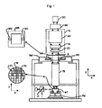
図1は、本発明の一実施形態によるリソグラフィ装置を概略的に描いている。装置は、放射ビームB(例えば、UV放射または他の任意の好適な放射)を調節するように構成された照明システム(イルミネータ)ILと、パターニングデバイス(例えばマスク)MAを支持するように構築され、かつ特定のパラメータに従ってパターニングデバイスを正確に位置決めするように構成された第一位置決めデバイスPMに接続されたマスク支持構造(例えばマスクテーブル)MTとを含む。装置はまた、基板(例えば、レジストコートウェーハ)Wを保持するように構築され、かつ特定のパラメータに従って基板を正確に位置決めするように構成された第二位置決めデバイスPWに接続された基板テーブル(例えば、ウェーハテーブル)WTまたは「基板サポート」を含む。装置は、放射ビームBに付与されるパターンを基板Wのターゲット部分C(例えば、1つまたは複数のダイを含む)にパターニングデバイスMAにより投影するように構成された投影システム(例えば、屈折投影レンズシステム)PSを更に含む。 FIG. 1 schematically depicts a lithographic apparatus according to an embodiment of the invention. The apparatus is constructed to support an illumination system (illuminator) IL configured to condition a radiation beam B (eg UV radiation or any other suitable radiation) and a patterning device (eg mask) MA And a mask support structure (e.g. mask table) MT connected to the first positioning device PM configured to accurately position the patterning device according to specific parameters. The apparatus is also configured to hold a substrate (e.g. a resist coated wafer) W, and a substrate table (e.g. connected to a second positioning device PW configured to accurately position the substrate according to certain parameters) , Wafer table) WT or "substrate support". The apparatus is a projection system (eg, refractive projection lens) configured to project a pattern imparted to the radiation beam B onto the target portion C of the substrate W (eg, including one or more dies) by the patterning device MA System) further includes PS.
照明システムは、放射の誘導、整形、または制御のための、屈折型、反射型、磁気型、電磁型、静電型または他のタイプの光学コンポーネント、またはこれらの任意の組み合わせなどの、種々のタイプの光学コンポーネントを含み得る。 The illumination system may include various types of optical components, such as refractive, reflective, magnetic, electromagnetic, electrostatic or other types of optical components, or any combination thereof, for the induction, shaping or control of radiation. It may include any type of optical component.
マスク支持構造は、パターニングデバイスを支持する、すなわちパターニングデバイスの重量を支える。マスク支持構造は、パターニングデバイスの向き、リソグラフィ装置の設計、および例えばパターニングデバイスが真空環境内に保持されるかどうかなどの他の条件に応じた様式でパターニングデバイスを保持する。マスク支持構造は、パターニングデバイスを保持するために、機械式、真空式、静電式または他のクランプ技術を使用することができる。マスク支持構造は、例えば、必要に応じて固定され得るまたは移動可能であり得る、フレームまたはテーブルであってもよい。マスク支持構造は、パターニングデバイスが、例えば投影システムに対して、所望の位置にあることを確実にし得る。本明細書での「レチクル」または「マスク」という用語のいかなる使用も、より一般的な用語である「パターニングデバイス」と同義であると見なしてよい。 The mask support structure supports the patterning device, ie bears the weight of the patterning device. The mask support structure holds the patterning device in a manner responsive to the orientation of the patterning device, the design of the lithographic apparatus, and other conditions, such as, for example, whether the patterning device is held in a vacuum environment. The mask support structure can use mechanical, vacuum, electrostatic or other clamping techniques to hold the patterning device. The mask support structure may be, for example, a frame or a table, which may be fixed or movable as required. The mask support structure may ensure that the patterning device is at a desired position, for example with respect to the projection system. Any use of the terms "reticle" or "mask" herein may be considered as synonymous with the more general term "patterning device."
本明細書で使用される「パターニングデバイス」という用語は、基板のターゲット部分にパターンを生成する目的で放射ビームの断面にパターンを付与するために使用できる任意のデバイスを指すものとして広く解釈されるべきである。例えばパターンが位相シフトフィーチャまたはいわゆるアシストフィーチャを含む場合に、放射ビームに付与されるパターンが基板のターゲット部分における所望のパターンに厳密には対応しない場合があることを留意すべきである。通例、放射ビームに付与されるパターンは、ターゲット部分に生成される集積回路のなどのデバイス内の特定の機能層に対応することになる。 The term "patterning device" as used herein is to be broadly interpreted as referring to any device that can be used to apply a pattern to the cross-section of a radiation beam for the purpose of generating a pattern on a target portion of a substrate It should. It should be noted that the pattern imparted to the radiation beam may not exactly correspond to the desired pattern in the target portion of the substrate, for example when the pattern comprises phase-shifting features or so called assist features. Typically, the pattern imparted to the radiation beam will correspond to a particular functional layer in the device, such as an integrated circuit produced on the target portion.
パターニングデバイスは、透過型または反射型であってもよい。パターニングデバイスの例としては、マスク、プログラマブルミラーアレイ、およびプログラマブルLCDパネルが挙げられる。マスクは、リソグラフィにおいて周知であるとともに、バイナリ、レベルソン型位相シフト、および減衰型位相シフトなどのマスクタイプ、ならびに種々のハイブリッドマスクタイプを含む。プログラマブルミラーアレイの一例では、小型ミラーのマトリクス配列が用いられ、小型ミラーの各々は、入射する放射ビームを異なる方向に反射するように個々に傾斜させることができる。傾斜したミラーは、ミラーマトリックスにより反射される放射ビームにパターンを付与する。 The patterning device may be transmissive or reflective. Examples of patterning devices include masks, programmable mirror arrays, and programmable LCD panels. Masks are well known in lithography and include binary, Lessonson phase shift, and mask types such as attenuated phase shift, as well as various hybrid mask types. An example of a programmable mirror array uses a matrix arrangement of small mirrors, each of which can be individually tilted so as to reflect an incoming radiation beam in different directions. The tilted mirrors impart a pattern to the radiation beam reflected by the mirror matrix.
本明細書で使用される「投影システム」という用語は、使用される露光放射に適したもの、または液浸液の使用もしくは真空の使用などのその他の要因に適したものとして、屈折型、反射型、反射屈折型、磁気型、電磁型および静電型光学システム、またはこれらの任意の組み合わせを含む、任意のタイプの投影システムを包含するものとして広く解釈されるべきである。本明細書での「投影レンズ」という用語のいかなる使用も、より一般的な用語である「投影システム」と同義であると見なしてよい。 The term "projection system" as used herein is refractive, reflective as suitable for the exposure radiation used, or other factors such as the use of immersion liquid or the use of a vacuum. It should be broadly interpreted as encompassing any type of projection system, including types, catadioptric, magnetic, electromagnetic and electrostatic optical systems, or any combination thereof. Any use of the term "projection lens" herein may be considered as synonymous with the more general term "projection system".
ここで描かれているように、装置は、透過型(例えば、透過型マスクを用いる)である。代替的に、装置は、反射型(例えば、上で言及したタイプのプログラマブルミラーアレイを用いるか、または反射マスクを用いる)であってもよい。 As depicted herein, the device is transmissive (eg, using a transmissive mask). Alternatively, the apparatus may be of a reflective type (e.g., using a programmable mirror array of a type as referred to above, or using a reflective mask).
リソグラフィ装置は、2つ(デュアルステージ)以上の基板テーブルもしくは「基板サポート」(および/または2つ以上のマスクテーブルもしくは「マスクサポート」)を有するタイプであってもよい。そのような「マルチステージ」機械では、追加のテーブルまたはサポートを並行して使用してもよく、あるいは、1つもしくは複数の他のテーブルまたはサポートを露光のために使用している間に、1つもしくは複数のテーブルまたはサポートに対して予備ステップを実行してもよい。 The lithographic apparatus may be of a type having two (dual stage) or more substrate tables or "substrate supports" (and / or two or more mask tables or "mask supports"). In such "multi-stage" machines, additional tables or supports may be used in parallel, or while one or more other tables or supports are being used for exposure 1 Preliminary steps may be performed on one or more tables or supports.
リソグラフィ装置はまた、投影システムと基板との間の空間を満たすために、比較的高い屈折率を有する液体、例えば水で基板の少なくとも一部分が覆われ得るタイプであってもよい。液浸液はまた、リソグラフィ装置内の他の空間に、例えば、マスクと投影システムとの間に適用されてもよい。液浸技術は、投影システムの開口数を増加させるために使用することができる。本明細書で使用される「液浸」という用語は、基板などの構造が液体に浸されなければならないことを意味するのではなく、露光中に投影システムと基板との間に液体が位置することを意味するに過ぎない。 The lithographic apparatus may also be of a type wherein at least a portion of the substrate may be covered by a liquid having a relatively high refractive index, eg water, so as to fill a space between the projection system and the substrate. Immersion liquid may also be applied to other spaces in the lithographic apparatus, for example, between the mask and the projection system. Immersion techniques can be used to increase the numerical aperture of projection systems. The term "immersion" as used herein does not mean that the structure, such as the substrate, has to be immersed in the liquid, but the liquid is located between the projection system and the substrate during exposure It just means that.
図1を参照すると、イルミネータILは、放射源SOから放射ビームを受け取る。例えば、放射源がエキシマレーザである場合には、放射源とリソグラフィ装置とが別体であってもよい。そのような場合に、放射源はリソグラフィ装置の一部を形成するとは見なされず、放射ビームは、例えば、好適な誘導ミラーおよび/またはビームエキスパンダを含むビームデリバリシステムBDの助けにより、放射源SOからイルミネータILに渡される。他の場合では、放射源は、例えば放射源が水銀ランプである場合、リソグラフィ装置の一体部であってもよい。必要であればビームデリバリシステムBDと共に、放射源SOおよびイルミネータILは、放射システムと呼ばれることがある。 Referring to FIG. 1, the illuminator IL receives a radiation beam from a radiation source SO. For example, if the source is an excimer laser, the source and the lithographic apparatus may be separate entities. In such cases, the radiation source is not considered to form part of the lithographic apparatus and the radiation beam is for example a radiation source SO with the aid of a beam delivery system BD comprising a suitable guiding mirror and / or a beam expander. It is passed to the illuminator IL. In other cases, the radiation source may be an integral part of the lithographic apparatus, for example when the radiation source is a mercury lamp. The source SO and the illuminator IL, together with the beam delivery system BD if required, may be referred to as a radiation system.
イルミネータILは、放射ビームの角度強度分布を調節するように構成されたアジャスタADを含み得る。通例では、イルミネータの瞳面内の強度分布の少なくとも外側および/または内側半径範囲(一般にそれぞれσ外側およびσ内側と呼ばれる)を調節することができる。加えて、イルミネータILは、インテグレータINおよびコンデンサCOなどの、他の種々のコンポーネントを含み得る。イルミネータは、ビーム断面における所望の均一性および強度分布を有するように放射ビームを調節するために使用されてもよい。 The illuminator IL may include an adjuster AD configured to adjust the angular intensity distribution of the radiation beam. Typically, at least the outer and / or inner radial extent (generally referred to as σ-outer and σ-inner, respectively) of the intensity distribution in the pupil plane of the illuminator can be adjusted. In addition, the illuminator IL may include various other components, such as an integrator IN and a capacitor CO. An illuminator may be used to adjust the radiation beam to have a desired uniformity and intensity distribution in the beam cross section.
放射ビームBは、マスク支持構造(例えば、マスクテーブルMT)上に保持される、パターニングデバイス(例えば、マスクMA)に入射して、パターニングデバイスによりパターンが付与される。マスクMAを通り抜けた後に、放射ビームBは投影システムPSを通過し、投影システムPSは基板Wのターゲット部分Cにビームの焦点を合わせる。第二位置決めデバイスPWおよび位置センサIF(例えば、干渉デバイス、リニアエンコーダまたは静電容量センサ)の助けにより、基板テーブルWTは、例えば、異なるターゲット部分Cを放射ビームBの経路に位置決めするように正確に移動させることができる。同様に、第一位置決めデバイスPMおよび別の位置センサ(図1には明示的に描かれていない)は、例えば、マスクライブラリの機械検索後に、またはスキャン中に、放射ビームBの経路に対してマスクMAを正確に位置決めするために使用することができる。概して、マスクテーブルMTの移動は、第一位置決めデバイスPMの一部を形成する、ロングストロークモジュール(粗動位置決め)およびショートストロークモジュール(微動位置決め)の助けにより実現されてもよい。同様に、基板テーブルWTまたは「基板サポート」の移動は、第二ポジショナPWの一部を形成する、ロングストロークモジュールおよびショートストロークモジュールを使用して実現されてもよい。ステッパの場合(スキャナとは対照的に)、マスクテーブルMTは、ショートストロークアクチュエータのみに接続されてもよく、または固定されてもよい。マスクMAおよび基板Wは、マスクアライメントマークM1、M2および基板アライメントマークP1、P2を使用して位置合わせされてもよい。図示の基板アライメントマークは専用のターゲット部分を占めるが、基板アライメントマークはターゲット部分間の空間に位置してもよい(これらはスクライブラインアライメントマークとして知られている)。同様に、2つ以上のダイがマスクMA上に設けられる状況では、マスクアライメントマークがダイの間に位置してもよい。 The radiation beam B is incident on the patterning device (e.g., mask MA), which is held on the mask support structure (e.g., mask table MT), and is patterned by the patterning device. After passing through the mask MA, the radiation beam B passes through the projection system PS, which focuses the beam on a target portion C of the substrate W. With the help of the second positioning device PW and the position sensor IF (e.g. an interference device, a linear encoder or a capacitance sensor), the substrate table WT is, for example, accurate to position different target portions C in the path of the radiation beam B Can be moved to Similarly, the first positioning device PM and another position sensor (not explicitly depicted in FIG. 1) are for example for the path of the radiation beam B after a machine search of the mask library or during a scan It can be used to accurately position the mask MA. In general, movement of the mask table MT may be realized with the aid of a long-stroke module (coarse positioning) and a short-stroke module (fine positioning), which form part of the first positioning device PM. Similarly, movement of the substrate table WT or "substrate support" may be realized using a long-stroke module and a short-stroke module, which form part of the second positioner PW. In the case of a stepper (as opposed to a scanner), the mask table MT may be connected only to the short stroke actuator or may be fixed. Mask MA and substrate W may be aligned using mask alignment marks M1, M2 and substrate alignment marks P1, P2. Although the illustrated substrate alignment marks occupy dedicated target portions, the substrate alignment marks may be located in the spaces between the target portions (these are known as scribe line alignment marks). Similarly, in situations in which more than one die is provided on the mask MA, the mask alignment marks may be located between the dies.
描かれている装置は、以下のモードのうちの少なくとも1つのモードで使用することができる。
1.ステップモードでは、マスクテーブルMTまたは「マスクサポート」および基板テーブルWTまたは「基板サポート」は基本的に静止状態に維持され、その一方で、放射ビームに付与されたパターン全体が1回でターゲット部分Cに投影される(すなわち、単一静的露光)。次いで、基板テーブルWTまたは「基板サポート」は、異なるターゲット部分Cを露光させることができるようにX方向および/またはY方向にずらされる。ステップモードでは、露光フィールドの最大サイズにより、単一静的露光で結像されるターゲット部分Cのサイズが制限される。
2.スキャンモードでは、マスクテーブルMTまたは「マスクサポート」および基板テーブルWTまたは「基板サポート」は同期してスキャンされ、その一方で、放射ビームに付与されたパターンがターゲット部分Cに投影される(すなわち、単一動的露光)。マスクテーブルMTまたは「マスクサポート」に対する基板テーブルWTまたは「基板サポート」の速度および方向は、投影システムPSの拡大(縮小)特性および像反転特性により決定されてもよい。スキャンモードでは、露光フィールドの最大サイズにより単一動的露光でのターゲット部分の(非スキャン方向における)幅が制限され、それに対して、スキャン動作の長さによりターゲット部分の(スキャン方向における)高さが決定される。
3.別のモードでは、マスクテーブルMTまたは「マスクサポート」は、プログラマブルパターニングデバイスを保持して基本的に静止状態に維持され、かつ放射ビームに付与されたパターンがターゲット部分Cに投影される間に基板テーブルWTまたは「基板サポート」が移動またはスキャンされる。このモードでは、通例はパルス放射源が用いられ、かつプログラマブルパターニングデバイスが基板テーブルWTまたは「基板サポート」の毎回の移動後にまたはスキャン中の連続する放射パルス間に必要に応じて更新される。この動作モードは、上で言及したタイプのプログラマブルミラーアレイなどの、プログラマブルパターニングデバイスを利用するマスクレスリソグラフィに容易に適用することができる。
The depicted apparatus can be used in at least one of the following modes:
1. In step mode, the mask table MT or "mask support" and the substrate table WT or "substrate support" are basically kept stationary, while the entire pattern imparted to the radiation beam is one target portion C at a time. Projected onto (ie, a single static exposure). The substrate table WT or "substrate support" is then offset in the X and / or Y direction so that different target portions C can be exposed. In step mode, the maximum size of the exposure field limits the size of the target portion C imaged in a single static exposure.
2. In scan mode, the mask table MT or "mask support" and the substrate table WT or "substrate support" are scanned synchronously while the pattern imparted to the radiation beam is projected onto the target portion C (ie Single dynamic exposure). The velocity and direction of the substrate table WT or "substrate support" relative to the mask table MT or "mask support" may be determined by the (de-) magnification and image reversal characteristics of the projection system PS. In scan mode, the maximum size of the exposure field limits the width (in the non-scan direction) of the target portion in a single dynamic exposure, whereas the length of the scan operation (in the scan direction) causes the height of the target portion Is determined.
3. In another mode, the mask table MT or "mask support" holds the programmable patterning device and remains essentially stationary, and the substrate while the pattern imparted to the radiation beam is projected onto the target portion C The table WT or "substrate support" is moved or scanned. In this mode, typically a pulsed radiation source is used and the programmable patterning device is updated after each movement of the substrate table WT or "substrate support" or as needed between successive radiation pulses during a scan. This mode of operation can be readily applied to maskless lithography that utilizes programmable patterning device, such as a programmable mirror array of a type as referred to above.
上で説明した使用モードの組み合わせおよび/もしくは変形、または全く異なる使用モードも用いることができる。 Combinations and / or variations on the above described modes of use or entirely different modes of use may also be used.
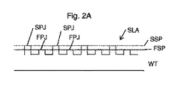
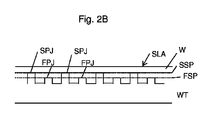
図2A〜図2Cは、基板テーブルWTの極めて概略的な側面図を描いている。基板テーブルWTは、複数の第一突出部FPJと複数の第二突出部SPJとを含む。突出部は、例えば、基板テーブル上の柱または他の任意の好適な突出部により形成されてもよい。突出部はまた、突出体と呼ばれることもある。基板テーブルWTには、基板Wが装填される基板装填領域SLAが設けられる。第一突出部は、基板装填領域SLAに広がっており、第一基板支持面FSPを画定する。第二突出部SPJもまた、基板装填領域SLAに広がっており、第二基板支持面SSPを画定する。第一基板支持面および第二基板支持面は、第一基板支持面と第二基板支持面とに垂直な(すなわち、直交する)方向に、互いに離間している、すなわち、間隔をおいて配置される。基板テーブルWTは、以下でより詳細に説明するように、基板Wをクランプするように、すなわち、基板テーブルに基板Wをクランプするために基板Wにクランプ力FCを加えるように構成されたクランプデバイスCDを更に含む。クランプデバイスCDは、基板に静電力を加える静電クランプデバイス、または基板に真空力を加える真空クランプデバイスなどの、任意のクランプデバイスであってもよい。 2A-2C depict a very schematic side view of the substrate table WT. The substrate table WT includes a plurality of first protrusions FPJ and a plurality of second protrusions SPJ. The protrusions may, for example, be formed by posts on the substrate table or any other suitable protrusions. The protrusions may also be referred to as protrusions. The substrate table WT is provided with a substrate loading area SLA in which a substrate W is loaded. The first protrusions extend into the substrate loading area SLA and define a first substrate support surface FSP. The second protrusions SPJ also extend into the substrate loading area SLA and define a second substrate support surface SSP. The first substrate support surface and the second substrate support surface are spaced apart from one another in a direction perpendicular (i.e. orthogonal) to the first substrate support surface and the second substrate support surface. Be done. The substrate table WT is configured to clamp the substrate W, ie to apply a clamping force FC to the substrate W to clamp the substrate W to the substrate table, as described in more detail below. It also contains a CD. The clamping device CD may be any clamping device, such as an electrostatic clamping device that applies an electrostatic force to the substrate, or a vacuum clamping device that applies a vacuum force to the substrate.
第二基板支持面SSPは、第一基板支持面FSPよりも基板テーブルから更に離れて位置する。第二突出部SPJは、第一基板支持面と第二基板支持面とに直交する方向に第一突出部FPJよりも更に延びる。結果として、基板テーブル上に基板を装填したときに、基板は最初に、図2Bに描かれているように、第二基板支持面SSPを画定する第二突出部SPJにより保持される。第二突出部は、ある程度の弾性を呈する、つまり、有限の堅牢性を有する。クランプデバイスCDによりクランプ力FCを加えたときに、第二突出部SPJが(例えば弾性)変形して、図2Cに描かれているように、第二基板支持面SSPに保持された状態から第一基板支持面FSPに保持された状態に基板Wを移動させる。したがって、基板テーブルWT上に基板Wを装填したときに、クランプ力FCを加える前には、基板Wは第二突出部SPJによってのみ支持される。その結果、基板テーブルWTによる摩擦力は、第二突出部SPJのインターフェースにおける摩擦力によってのみ定められる。クランプ力FCにより基板Wをクランプしたときに、基板Wは、第一基板装填表面FSPに移動し、ここで、基板Wは第一突出部と第二突出部により支持される。したがって、基板テーブルWTによる摩擦は、第一突出部と第二突出部とにより定められる。結果として、基板Wをクランプする前は、基板Wをクランプしたときよりも摩擦力が低いので、第一の場合と同じように、第二突出部SPJのみが摩擦に寄与し、その一方で、第二の場合では、第一突出部と第二突出部の両方が基板Wのインターフェースにおける摩擦力に寄与する。したがって、基板Wの装填時に、低応力負荷を促進するために比較的低い摩擦が与えられてもよく、その一方で、クランプ時に、基板Wの照射誘導(局所)加熱時でさえ、定められた位置決めを促進するために比較的高い摩擦力が与えられてもよい。したがって、装填時に低摩擦を必要とする基板Wの低応力負荷が、高摩擦クランプを必要とする、クランプ時の定められた正確な位置決めと組み合わされてもよい。更に、本発明の結果として、クランプ時に基板Wと基板テーブルWTとの接触面が増加することがあり、こうした接触面の増加が、基板テーブルWTに基板Wをクランプするのにファンデルワールス力を利用することを可能にし得る。本発明によれば、第一基板支持面FSPが第一突出部FPJにより画定される一方で、第二基板支持面SSPは第二突出部SPJにより画定される。 The second substrate support surface SSP is located further from the substrate table than the first substrate support surface FSP. The second protrusion SPJ extends further than the first protrusion FPJ in a direction orthogonal to the first substrate support surface and the second substrate support surface. As a result, when loading the substrate onto the substrate table, the substrate is first held by the second protrusions SPJ defining the second substrate support surface SSP, as depicted in FIG. 2B. The second projection exhibits a certain degree of elasticity, ie it has a finite robustness. When a clamping force FC is applied by the clamping device CD, the second projection SPJ is deformed (for example, elastically) to be held from the second substrate support surface SSP as illustrated in FIG. 2C. The substrate W is moved to a state of being held by one substrate support surface FSP. Therefore, when the substrate W is loaded onto the substrate table WT, the substrate W is supported only by the second projection SPJ before applying the clamping force FC. As a result, the friction force by the substrate table WT is determined only by the friction force at the interface of the second projection SPJ. When the substrate W is clamped by the clamping force FC, the substrate W moves to the first substrate loading surface FSP, where the substrate W is supported by the first and second protrusions. Thus, the friction due to the substrate table WT is determined by the first and second protrusions. As a result, before clamping the substrate W, since the frictional force is lower than when clamping the substrate W, as in the first case, only the second projection SPJ contributes to the friction, while In the second case, both the first and second protrusions contribute to the frictional force at the interface of the substrate W. Thus, when loading the substrate W, a relatively low friction may be provided to promote low stress loading, while at the time of clamping it is defined even during irradiation-induced (local) heating of the substrate W. Relatively high friction may be provided to facilitate positioning. Thus, the low stress loading of the substrate W, which requires low friction at the time of loading, may be combined with a defined exact positioning at the time of clamping, which requires a high friction clamp. Furthermore, as a result of the present invention, the contact surface between the substrate W and the substrate table WT may increase during clamping, which increases the van der Waals force for clamping the substrate W onto the substrate table WT. May make it possible to use. According to the invention, the first substrate support surface FSP is defined by the first protrusion FPJ, while the second substrate support surface SSP is defined by the second protrusion SPJ.
本文書で説明される概念が、基板テーブルにより保持すべき平面状裏面を有する基板に対して、および異形裏面を有する基板に対して適用され得ることに留意されたい。基板が異形裏面を有する場合には、第一突出部および第二突出部の上面により画定される第一基板支持面および第二基板支持面は、相応に異形とされてもよい。この概念に従う材料は、SiC、Si、SiO2、DLC(ダイアモンドライクコーティング)被覆基板、窒化物被覆基板、Al2O3、およびリソグラフィ産業で現在使用されている他の材料であってもよい。突出部は、任意の好適な方法で、例えば、フォトリソグラフィおよびレーザ加工により作製されてもよい。(図3Aおよび図3Bを参照して以下に述べる)基板テーブルのバールも、例えば、フォトリソグラフィおよびレーザ加工によって作製され得るので、同様または同じ処理が適用されてもよい。 It should be noted that the concepts described in this document can be applied to a substrate having a planar back surface to be held by the substrate table and to a substrate having a back surface profile. If the substrate has a profiled back surface, the first substrate support surface and the second substrate support surface defined by the top surfaces of the first and second protrusions may be correspondingly profiled. Materials in accordance with this concept may be SiC, Si, SiO 2, DLC (diamond like coating) coated substrates, nitride coated substrates, Al 2 O 3 , and other materials currently used in the lithography industry. The protrusions may be made in any suitable manner, for example by photolithography and laser processing. Similar or the same processing may be applied as the substrate table burls (discussed below with reference to FIGS. 3A and 3B) may also be made, for example, by photolithography and laser processing.
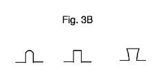
図3Aは、本発明の実施形態による基板テーブルWTの一部の詳細図を描いている。基板テーブルWTは、基板Wを搬送するように構成された、複数のバールBRLを含む。複数のバールBRLは、搬送すべき基板と実質的に等しいかまたはそれよりも大きな領域に広がっていてもよい。実施形態におけるバールBRLには、図2A〜図2Cを参照して説明してきた第一および第二突出部と同様の、複数の第一突出部FPJおよび第二突出部SPJが各々設けられる。よって、基板Wの装填時に、各バールBRLの第二突出部SPJが基板Wに接触し、その間、クランプデバイスによりクランプ力を加えたときに、第二突出部SPJが変形して、第二基板支持面SSPから第一基板支持面FSPに基板を移動させ、よって、基板が各バールの第一突出部と第二突出部の両方により保持される。図3Bに描かれているように、第二突出部SPJには、搬送すべき基板に向かい合う球面状SPH上面または搬送すべき基板に向かい合う平面状FLA上面が設けられてもよい。更に、第二突出部SPJには「キノコ型」MSH形状が設けられてもよく、それにより、第二突出部SPJの断面が、搬送すべき基板に向かう方向に増加する。第一突出部および第二突出部は、異なるアスペクト比を有するような寸法とされてもよい。第二突出部SPJの形状は、摩擦力に影響を及ぼすことができる。例えば、キノコ型形状の利点は、より大きな接触領域に起因してウェーハインターフェースでの摩擦力がより高くなることである。 FIG. 3A depicts a detailed view of a portion of a substrate table WT in accordance with an embodiment of the present invention. The substrate table WT includes a plurality of burls BRL configured to transport the substrate W. The plurality of burls BRL may extend over an area substantially equal to or larger than the substrate to be transported. In the embodiment, the burl BRL is provided with a plurality of first protrusions FPJ and second protrusions SPJ similar to the first and second protrusions described with reference to FIGS. 2A to 2C. Therefore, when the substrate W is loaded, the second protrusions SPJ of the respective burls BRL contact the substrate W, and during that time, when the clamping force is applied by the clamp device, the second protrusions SPJ deform and the second substrate The substrate is moved from the support surface SSP to the first substrate support surface FSP so that the substrate is held by both the first and second projections of each bur. As depicted in FIG. 3B, the second protrusion SPJ may be provided with a spherical SPH upper surface facing the substrate to be transported or a planar FLA upper surface facing the substrate to be transported. Furthermore, the second projection SPJ may be provided with a "mushroom-shaped" MSH shape, whereby the cross-section of the second projection SPJ increases in the direction towards the substrate to be transported. The first and second protrusions may be sized to have different aspect ratios. The shape of the second projection SPJ can influence the frictional force. For example, an advantage of the mushroom shaped shape is that the friction at the wafer interface is higher due to the larger contact area.
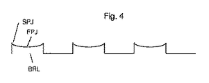
図4は、本発明の別の実施形態による基板テーブルの一部の詳細図を描いている。基板テーブルWTは、基板を搬送するように構成された、複数のバールBRLを含む。複数のバールBRLは、搬送すべき基板と実質的に等しいかまたはそれよりも大きな領域に広がっていてもよい。図4による実施形態におけるバールBRLには各々、上面、すなわち、第二基板装填表面SSPに向かい合うバールの表面が設けられ、この上面は凹形状を有する。それにより、凹状面の周縁部におけるバールBRLの周方向外側部が第二突出部SPJを形成し、その一方で、バールの残りの部分、すなわち中央部が、第一突出部FPJを形成する。それにより、横方向の堅牢性が大きくなることがある。材料の例は、比較的歪み耐性があるDLC(a:c−H)被覆基板などの高いH/E=0.1−016(H:硬度、E:弾性率)を有する材料であってもよい。 FIG. 4 depicts a detailed view of a portion of a substrate table according to another embodiment of the present invention. The substrate table WT includes a plurality of burls BRL configured to transport a substrate. The plurality of burls BRL may extend over an area substantially equal to or larger than the substrate to be transported. Each of the burls BRL in the embodiment according to FIG. 4 is provided with a top surface, ie the surface of the burls facing the second substrate loading surface SSP, which has a concave shape. Thereby, the circumferentially outer part of the burl BRL in the peripheral part of the concave surface forms the second projecting part SPJ, while the remaining part of the burl, ie the central part, forms the first projecting part FPJ. This may increase lateral robustness. An example of the material is even a material with high H / E = 0.1 to 016 (H: hardness, E: elastic modulus), such as a relatively strain resistant DLC (a: cH) coated substrate. Good.
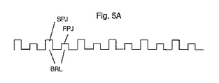
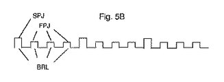
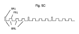
図5A〜図5Cは、本発明の更なる実施形態による基板テーブルの一部の詳細図を描いている。これらの実施形態において、第一突出部FPJおよび第二突出部SPJは、基板を搬送するように構成された複数のバールBRLを形成する。よって、第一突出部および第二突出部は、搬送すべき基板と実質的に等しいかまたはそれよりも大きな領域に広がっていてもよい。実施形態におけるバールBRLは、複数の第一突出部FPJおよび第二突出部SPJにより形成される。図5Aに概略的に描かれている実施形態では、第一突出部FPJの量が第二突出部SPJの量にほぼ等しく、第一突出部および第二突出部が間欠的に配置される。第一突出部FPJの直径は、第二突出部SPJの直径と異なってもよい。例えば、第二突出部SPJの直径は、第一突出部FPJの直径よりも小さくてもよい。図5Bは、第一突出部FPJの量が第二突出部SPJの量よりも多い実施形態を描いている。例えば、3つの第一突出部FPJ毎に、第二突出部SPJが1つ設けられる。そのような実施形態において、クランプ時に得られる摩擦は、第二突出部SPJの量が第一突出部FPJの量よりもかなり多いことを考慮すると、装填時得られる摩擦よりもかなり高くなる可能性がある。同様の効果は、第一基板支持面および第二基板支持面に沿った方向に見られる第二突出部SPJの直径(ひいては基板に向かい合う第二突出部SPJの接触面)が、第一基板支持面および第二基板支持面に沿った方向に見られる、第一突出部FPJの直径ひいては接触領域よりも小さい、図5Cに描かれている実施形態により得られることがある。この構成の利点は、この構成が接触領域およびバール堅牢性に応じて基板装填および基板クランプでの摩擦を調整することを可能にし得ることである。 5A-5C depict a detailed view of a portion of a substrate table according to a further embodiment of the present invention. In these embodiments, the first projection FPJ and the second projection SPJ form a plurality of burls BRL configured to transport the substrate. Thus, the first and second protrusions may extend over an area substantially equal to or larger than the substrate to be transported. The burl BRL in the embodiment is formed by the plurality of first protrusions FPJ and the second protrusions SPJ. In the embodiment schematically depicted in FIG. 5A, the amount of the first protrusions FPJ is approximately equal to the amount of the second protrusions SPJ, and the first protrusions and the second protrusions are arranged intermittently. The diameter of the first protrusion FPJ may be different from the diameter of the second protrusion SPJ. For example, the diameter of the second protrusion SPJ may be smaller than the diameter of the first protrusion FPJ. FIG. 5B depicts an embodiment in which the amount of first protrusions FPJ is greater than the amount of second protrusions SPJ. For example, one second protrusion SPJ is provided for every three first protrusions FPJ. In such an embodiment, the friction obtained upon clamping may be much higher than the friction obtained upon loading, given that the amount of the second projection SPJ is much greater than the amount of the first projection FPJ. There is. A similar effect is that the diameter of the second protrusion SPJ seen in the direction along the first substrate support surface and the second substrate support surface (and hence the contact surface of the second protrusion SPJ facing the substrate) is the first substrate support. It may be obtained by the embodiment depicted in FIG. 5C, which is smaller than the diameter and thus the contact area of the first projection FPJ seen in the direction along the surface and the second substrate support surface. An advantage of this configuration is that it may allow to adjust the friction at the substrate loading and substrate clamp depending on the contact area and the burls robustness.
本文ではICの製造におけるリソグラフィ装置の使用についての具体的な言及がなされ得るが、本明細書で説明するリソグラフィ装置が、集積光学システム、磁気ドメインメモリ用の誘導および検出パターン、フラットパネルディスプレイ、液晶ディスプレイ(LCD)、薄膜磁気ヘッドなどの製造などの、他の用途を有し得ることを理解すべきである。当業者であれば、そのような代替的な用途の文脈では、本明細書での「ウェーハ」または「ダイ」という用語のいかなる使用も、より一般的な用語である「基板」または「ターゲット部分」とそれぞれ同義であると見なされ得ることを認識するであろう。本明細書で言及される基板は、露光前または露光後に、例えばトラック(典型的にはレジスト層を基板に塗布し、露光されたレジストを現像するツール)、メトロロジツールおよび/またはインスペクションツールで処理されてもよい。適用可能であれば、本明細書における開示は、そのような基板プロセシングツールおよび他の基板プロセシングツールに適用されてもよい。更に、基板は、例えば、積層ICを生成するために、2回以上処理され得るので、本明細書で使用される基板という用語は、処理された複数の層を既に含む基板を指すこともある。 Although specific reference may be made herein to the use of a lithographic apparatus in the manufacture of ICs, the lithographic apparatus described herein may be integrated optical systems, inductive and detection patterns for magnetic domain memories, flat panel displays, liquid crystals It should be understood that it may have other applications, such as the manufacture of displays (LCDs), thin film magnetic heads, etc. One skilled in the art, in the context of such alternative applications, any use of the terms "wafer" or "die" herein is the more general term "substrate" or "target portion". It will be appreciated that each may be considered as synonymous. The substrates referred to herein may be, for example, tracks (typically a tool for applying a resist layer to a substrate and developing the exposed resist), a metrology tool and / or an inspection tool before or after exposure. It may be processed. Where applicable, the disclosure herein may be applied to such substrate processing tools and other substrate processing tools. Furthermore, the term substrate as used herein may also refer to a substrate already comprising a plurality of layers processed, as the substrate may be processed more than once, for example, to produce a laminated IC. .
光リソグラフィの文脈での本発明の実施形態の使用についての具体的な言及が上記でなされたが、本発明が他の用途、例えばインプリントリソグラフィに使用され得ることと、文脈が許す限り、本発明が光リソグラフィに限定されないことが認識されるであろう。インプリントリソグラフィでは、パターニングデバイスにおけるトポグラフィが基板上に生成されるパターンを画定する。パターニングデバイスのトポグラフィは、基板に供給されたレジスト層に押し込まれてもよく、その後、電磁放射、熱、圧力またはこれらの組み合わせを加えることによりレジストを硬化させる。パターニングデバイスは、レジストが硬化された後に、レジストから外されて、レジストにパターンを残す。 Although specific reference has been made above to the use of embodiments of the invention in the context of optical lithography, to the extent that the invention may be used in other applications, such as imprint lithography, and the context allows, It will be appreciated that the invention is not limited to optical lithography. In imprint lithography a topography in a patterning device defines the pattern created on a substrate. The topography of the patterning device may be pressed into a layer of resist supplied to the substrate whereupon the resist is cured by applying electromagnetic radiation, heat, pressure or a combination thereof. The patterning device is removed from the resist after the resist is cured, leaving a pattern in the resist.
本明細書で使用される「放射」および「ビーム」という用語は、紫外線(UV)放射(例えば、365、248、193、157もしくは126nmまたはそれらの近辺の波長を有する)および極端紫外線(EUV)放射(例えば、5〜20nmの範囲の波長を有する)、ならびにイオンビームまたは電子ビームなどの、粒子ビームを含む、全てのタイプの電磁放射を包含する。 The terms "radiation" and "beam" as used herein are ultraviolet (UV) radiation (e.g. having a wavelength of 365, 248, 193, 157 or 126 nm or near) and extreme ultraviolet (EUV) It encompasses all types of electromagnetic radiation, including radiation (eg, having a wavelength in the range of 5-20 nm), as well as particle beams, such as ion or electron beams.
「レンズ」という用語は、文脈が許す限り、屈折型、反射型、磁気型、電磁型および静電型光学コンポーネントを含む、種々のタイプの光学コンポーネントの任意の1つまたは組み合わせを指すことがある。 The term "lens", where the context allows, may refer to any one or combination of various types of optical components, including refractive, reflective, magnetic, electromagnetic and electrostatic optical components .
本発明の具体的な実施形態を上で説明してきたが、上で説明した以外の仕方で本発明が実施され得ることが認識されよう。例えば、本発明は、上で開示した方法を記述する機械可読命令の1つもしくは複数のシーケンスを含むコンピュータプログラム、またはかかるコンピュータプログラムが記憶されたデータ記録媒体(例えば、半導体メモリ、磁気ディスクもしくは光ディスク)の形態をとってもよい。 While specific embodiments of the invention have been described above, it will be appreciated that the invention may be practiced otherwise than as described. For example, the present invention relates to a computer program comprising one or more sequences of machine-readable instructions describing the method disclosed above, or a data storage medium (e.g. a semiconductor memory, magnetic disk or optical disk) on which such computer program is stored. It may take the form of).
上の説明は、限定的なものではなく例示的なものと意図されている。したがって、以下に記載する特許請求の範囲から逸脱することなく、説明した本発明に修正を加え得ることは、当業者には明らかであろう。 The above description is intended to be illustrative rather than limiting. Thus, it will be apparent to one skilled in the art that modifications may be made to the invention as described without departing from the scope of the claims set out below.
Claims (11)
第一基板支持面を画定する、複数の第一突出部と、
第二基板支持面を画定する、複数の第二突出部と、
前記基板にクランプ力を及ぼすように構成されたクランプデバイスとを含み、
前記第二基板支持面が前記第一基板支持面に平行であり、前記第二基板支持面が、前記第一基板支持面と前記第二基板支持面とに直交する方向に前記第一基板支持面に対してずらされており、
前記リソグラフィ装置用基板テーブルが、前記クランプデバイスにより前記クランプ力を加える前に前記第二基板支持面における前記第二突出部上に前記基板を支持するように構成され、
第二突出部が、前記クランプデバイスにより前記基板に前記クランプ力を加えると変形するように構成され、それにより、前記クランプデバイスにより前記基板がクランプされたときに前記基板を前記第二基板支持面から前記第一基板支持面に移動させる、
リソグラフィ装置用基板テーブル。 A substrate table for a lithographic apparatus constructed to hold a substrate, the substrate table comprising:
A plurality of first protrusions defining a first substrate support surface;
A plurality of second protrusions defining a second substrate support surface;
And a clamping device configured to exert a clamping force on the substrate,
The second substrate support surface is parallel to the first substrate support surface, and the second substrate support surface is perpendicular to the first substrate support surface and the second substrate support surface. Offset with respect to the surface,
The substrate table for a lithographic apparatus is configured to support the substrate on the second projection on the second substrate support surface before applying the clamping force by the clamping device;
A second projection is configured to deform upon application of the clamping force to the substrate by the clamping device, whereby the substrate is supported by the second substrate support surface when the substrate is clamped by the clamping device. To the first substrate support surface from the
Substrate table for lithographic apparatus.
第一基板支持面を画定する、複数の第一突出部と、第二基板支持面を画定する、複数の第二突出部と、前記基板にクランプ力を及ぼすように構成されたクランプデバイスとを含み、前記第二基板支持面が前記第一基板支持面に平行であり、前記第二基板支持面が、前記第一基板支持面と前記第二基板支持面とに直交する方向に前記第一基板支持面に対してずらされている、基板テーブルを準備することと、
前記クランプデバイスにより前記クランプ力を加える前に、前記第二基板支持面における前記第二突出部上に前記基板を支持することと、
前記クランプデバイスにより前記基板に前記クランプ力を加えて前記第二突出部を変形させ、それにより、前記クランプデバイスにより前記基板がクランプされたときに前記基板を前記第二基板支持面から前記第一基板支持面に移動させることと
を含む、基板の装填方法。 A method of loading a substrate onto a substrate table of a lithographic apparatus, the method comprising:
A plurality of first protrusions defining a first substrate support surface, a plurality of second protrusions defining a second substrate support surface, and a clamping device configured to exert a clamping force on the substrate The second substrate support surface is parallel to the first substrate support surface, and the first substrate support surface is perpendicular to the first substrate support surface and the second substrate support surface. Preparing a substrate table offset relative to the substrate support surface;
Supporting the substrate on the second projection on the second substrate support surface prior to applying the clamping force by the clamping device;
The clamping device applies the clamping force to the substrate by the clamping device to deform the second projection, whereby the substrate is clamped from the second substrate support surface when the substrate is clamped by the clamping device. Moving the substrate to the substrate support surface.
Priority Applications (2)
| Application Number | Priority Date | Filing Date | Title |
|---|---|---|---|
| JP2020069583A JP6977099B2 (en) | 2015-10-29 | 2020-04-08 | Board table for lithography equipment and how to load the board |
| JP2021183059A JP7378453B2 (en) | 2015-10-29 | 2021-11-10 | Substrate table for lithography equipment and method for loading substrates |
Applications Claiming Priority (3)
| Application Number | Priority Date | Filing Date | Title |
|---|---|---|---|
| EP15192099.8 | 2015-10-29 | ||
| EP15192099 | 2015-10-29 | ||
| PCT/EP2016/073033 WO2017071900A1 (en) | 2015-10-29 | 2016-09-28 | Lithographic apparatus substrate table and method of loading a substrate |
Related Child Applications (1)
| Application Number | Title | Priority Date | Filing Date |
|---|---|---|---|
| JP2020069583A Division JP6977099B2 (en) | 2015-10-29 | 2020-04-08 | Board table for lithography equipment and how to load the board |
Publications (1)
| Publication Number | Publication Date |
|---|---|
| JP2018533763A true JP2018533763A (en) | 2018-11-15 |
Family
ID=54364133
Family Applications (3)
| Application Number | Title | Priority Date | Filing Date |
|---|---|---|---|
| JP2018518722A Pending JP2018533763A (en) | 2015-10-29 | 2016-09-28 | Substrate table for lithographic apparatus and method of loading a substrate |
| JP2020069583A Active JP6977099B2 (en) | 2015-10-29 | 2020-04-08 | Board table for lithography equipment and how to load the board |
| JP2021183059A Active JP7378453B2 (en) | 2015-10-29 | 2021-11-10 | Substrate table for lithography equipment and method for loading substrates |
Family Applications After (2)
| Application Number | Title | Priority Date | Filing Date |
|---|---|---|---|
| JP2020069583A Active JP6977099B2 (en) | 2015-10-29 | 2020-04-08 | Board table for lithography equipment and how to load the board |
| JP2021183059A Active JP7378453B2 (en) | 2015-10-29 | 2021-11-10 | Substrate table for lithography equipment and method for loading substrates |
Country Status (4)
| Country | Link |
|---|---|
| US (2) | US10236203B2 (en) |
| JP (3) | JP2018533763A (en) |
| NL (1) | NL2017542A (en) |
| WO (1) | WO2017071900A1 (en) |
Cited By (2)
| Publication number | Priority date | Publication date | Assignee | Title |
|---|---|---|---|---|
| JP2022533319A (en) * | 2019-05-24 | 2022-07-22 | エーエスエムエル ホールディング エヌ.ブイ. | Lithographic apparatus, substrate table and method |
| JP2023004984A (en) * | 2021-06-25 | 2023-01-17 | セメス カンパニー,リミテッド | Support unit, bake apparatus including the same and substrate processing apparatus |
Families Citing this family (5)
| Publication number | Priority date | Publication date | Assignee | Title |
|---|---|---|---|---|
| US11270906B2 (en) * | 2017-10-27 | 2022-03-08 | Asml Holding N.V. | Burls with altered surface topography for holding an object in lithography applications |
| JP6917523B2 (en) | 2017-11-08 | 2021-08-11 | エーエスエムエル ネザーランズ ビー.ブイ. | Board holders and methods for manufacturing board holders |
| EP3915142A1 (en) * | 2019-01-23 | 2021-12-01 | ASML Netherlands B.V. | Substrate holder for use in a lithographic apparatus and a device manufacturing method |
| US20230359118A1 (en) * | 2020-04-03 | 2023-11-09 | Asml Holding N.V. | Systems and methods for forming structures on a surface |
| US12560872B2 (en) * | 2020-12-29 | 2026-02-24 | Asml Netherlands B.V. | Vacuum sheet bond fixturing and flexible burl applications for substrate tables |
Citations (13)
| Publication number | Priority date | Publication date | Assignee | Title |
|---|---|---|---|---|
| JPS59195826A (en) * | 1983-04-21 | 1984-11-07 | Toshiba Corp | Resist applying apparatus |
| JPS6426648U (en) * | 1987-07-08 | 1989-02-15 | ||
| JPH0312948A (en) * | 1989-06-12 | 1991-01-21 | Nikon Corp | Substrate holder |
| JPH0414239A (en) * | 1990-05-07 | 1992-01-20 | Canon Inc | Vacuum sucking system wafer retaining equipment |
| JPH10242255A (en) * | 1997-02-28 | 1998-09-11 | Kyocera Corp | Vacuum suction device |
| JP2004228453A (en) * | 2003-01-27 | 2004-08-12 | Renesas Technology Corp | Method of manufacturing semiconductor device |
| JP2005032977A (en) * | 2003-07-14 | 2005-02-03 | Nikon Corp | Vacuum chuck |
| JP2005228978A (en) * | 2004-02-13 | 2005-08-25 | Canon Inc | Exposure apparatus and semiconductor device manufacturing method |
| JP2006339347A (en) * | 2005-06-01 | 2006-12-14 | Canon Inc | Reticle chuck |
| JP2007207842A (en) * | 2006-01-31 | 2007-08-16 | Sumitomo Osaka Cement Co Ltd | Electrostatic chuck device |
| JP2007273693A (en) * | 2006-03-31 | 2007-10-18 | Nikon Corp | Substrate holding member, substrate holding method, substrate holding apparatus, exposure apparatus, and exposure method |
| JP2010515258A (en) * | 2006-12-27 | 2010-05-06 | エーエスエムエル ネザーランズ ビー.ブイ. | Lithographic apparatus, substrate table, and method for improving substrate release characteristics |
| JP2012079829A (en) * | 2010-09-30 | 2012-04-19 | Covalent Materials Corp | Refrigeration pin chuck |
Family Cites Families (30)
| Publication number | Priority date | Publication date | Assignee | Title |
|---|---|---|---|---|
| JPH0625263B2 (en) | 1987-07-23 | 1994-04-06 | 工業技術院長 | Method for treating conductive polymer film |
| DE69133413D1 (en) * | 1990-05-07 | 2004-10-21 | Canon Kk | Vacuum type substrate support |
| JP2002134599A (en) | 2000-10-24 | 2002-05-10 | Ngk Insulators Ltd | Electrostatic chuck apparatus |
| EP1482370B1 (en) * | 2003-05-06 | 2012-02-01 | ASML Netherlands B.V. | Substrate holder for lithographic apparatus |
| EP1491953A1 (en) | 2003-06-23 | 2004-12-29 | ASML Netherlands B.V. | Lithographic apparatus, device manufacturing method, and device manufactured thereby |
| US7133120B2 (en) * | 2004-05-04 | 2006-11-07 | Asml Netherlands B.V. | Lithographic apparatus, article support member, and method |
| US7050147B2 (en) * | 2004-07-08 | 2006-05-23 | Asml Netherlands B.V. | Method of adjusting a height of protrusions on a support surface of a support table, a lithographic projection apparatus, and a support table for supporting an article in a lithographic apparatus |
| US7532310B2 (en) * | 2004-10-22 | 2009-05-12 | Asml Netherlands B.V. | Apparatus, method for supporting and/or thermally conditioning a substrate, a support table, and a chuck |
| US7564536B2 (en) | 2005-11-08 | 2009-07-21 | Asml Netherlands B.V. | Lithographic apparatus and device manufacturing method |
| US7646581B2 (en) * | 2006-01-31 | 2010-01-12 | Sumitomo Osaka Cement Co., Ltd. | Electrostatic chuck |
| US8284379B2 (en) * | 2007-04-06 | 2012-10-09 | Nikon Corporation | Devices and methods for reducing residual reticle chucking forces |
| US8218284B2 (en) | 2008-07-24 | 2012-07-10 | Hermes-Microvision, Inc. | Apparatus for increasing electric conductivity to a semiconductor wafer substrate when exposure to electron beam |
| NL2003470A (en) | 2008-10-07 | 2010-04-08 | Asml Netherlands Bv | Lithographic apparatus and device manufacturing method. |
| NL2004545A (en) * | 2009-06-09 | 2010-12-13 | Asml Netherlands Bv | Lithographic method and arrangement |
| KR101109822B1 (en) | 2010-01-26 | 2012-02-13 | 주식회사 엘지실트론 | Wafer support pin and its manufacturing method which can reduce dislocation defects during wafer heat treatment |
| JP5775148B2 (en) * | 2010-04-23 | 2015-09-09 | エーエスエムエル ネザーランズ ビー.ブイ. | Method and lithographic apparatus for loading a substrate |
| JP5810517B2 (en) * | 2010-12-02 | 2015-11-11 | 富士電機株式会社 | Adsorption device and adsorption method |
| WO2012110144A1 (en) | 2011-02-18 | 2012-08-23 | Asml Netherlands B.V. | Lithographic apparatus and device manufacturing method. |
| AT511627B1 (en) * | 2011-07-01 | 2015-05-15 | Mechatronic Systemtechnik Gmbh | DEVICE FOR HOLDING A SURFACE SUBSTRATE |
| NL2009189A (en) * | 2011-08-17 | 2013-02-19 | Asml Netherlands Bv | Support table for a lithographic apparatus, lithographic apparatus and device manufacturing method. |
| NL2009874A (en) * | 2011-12-23 | 2013-06-26 | Asml Netherlands Bv | Support, lithographic apparatus and device manufacturing method. |
| KR101979893B1 (en) * | 2012-05-29 | 2019-05-17 | 에이에스엠엘 네델란즈 비.브이. | Object holder and lithographic apparatus |
| WO2014103714A1 (en) | 2012-12-25 | 2014-07-03 | 京セラ株式会社 | Attachment member and attachment device using the same |
| US9543186B2 (en) * | 2013-02-01 | 2017-01-10 | Applied Materials, Inc. | Substrate support with controlled sealing gap |
| US9835957B2 (en) * | 2013-09-27 | 2017-12-05 | Asml Netherlands B.V. | Support table for a lithographic apparatus, lithographic apparatus and device manufacturing method |
| KR101885750B1 (en) * | 2014-01-20 | 2018-08-06 | 에이에스엠엘 네델란즈 비.브이. | Substrate holder and support table for lithography |
| JP6212412B2 (en) | 2014-02-28 | 2017-10-11 | 日本特殊陶業株式会社 | Vacuum suction member |
| JP6369054B2 (en) | 2014-03-03 | 2018-08-08 | 東京エレクトロン株式会社 | Substrate placing apparatus and substrate processing apparatus |
| US9798253B2 (en) * | 2014-04-30 | 2017-10-24 | Asml Netherlands B.V. | Support table for a lithographic apparatus, lithographic apparatus and device manufacturing method |
| WO2017001135A1 (en) * | 2015-07-02 | 2017-01-05 | Asml Netherlands B.V. | A substrate holder, a lithographic apparatus and method of manufacturing devices |
-
2016
- 2016-09-28 US US15/767,514 patent/US10236203B2/en not_active Ceased
- 2016-09-28 WO PCT/EP2016/073033 patent/WO2017071900A1/en not_active Ceased
- 2016-09-28 JP JP2018518722A patent/JP2018533763A/en active Pending
- 2016-09-28 US US16/666,485 patent/USRE50785E1/en active Active
- 2016-09-28 NL NL2017542A patent/NL2017542A/en unknown
-
2020
- 2020-04-08 JP JP2020069583A patent/JP6977099B2/en active Active
-
2021
- 2021-11-10 JP JP2021183059A patent/JP7378453B2/en active Active
Patent Citations (13)
| Publication number | Priority date | Publication date | Assignee | Title |
|---|---|---|---|---|
| JPS59195826A (en) * | 1983-04-21 | 1984-11-07 | Toshiba Corp | Resist applying apparatus |
| JPS6426648U (en) * | 1987-07-08 | 1989-02-15 | ||
| JPH0312948A (en) * | 1989-06-12 | 1991-01-21 | Nikon Corp | Substrate holder |
| JPH0414239A (en) * | 1990-05-07 | 1992-01-20 | Canon Inc | Vacuum sucking system wafer retaining equipment |
| JPH10242255A (en) * | 1997-02-28 | 1998-09-11 | Kyocera Corp | Vacuum suction device |
| JP2004228453A (en) * | 2003-01-27 | 2004-08-12 | Renesas Technology Corp | Method of manufacturing semiconductor device |
| JP2005032977A (en) * | 2003-07-14 | 2005-02-03 | Nikon Corp | Vacuum chuck |
| JP2005228978A (en) * | 2004-02-13 | 2005-08-25 | Canon Inc | Exposure apparatus and semiconductor device manufacturing method |
| JP2006339347A (en) * | 2005-06-01 | 2006-12-14 | Canon Inc | Reticle chuck |
| JP2007207842A (en) * | 2006-01-31 | 2007-08-16 | Sumitomo Osaka Cement Co Ltd | Electrostatic chuck device |
| JP2007273693A (en) * | 2006-03-31 | 2007-10-18 | Nikon Corp | Substrate holding member, substrate holding method, substrate holding apparatus, exposure apparatus, and exposure method |
| JP2010515258A (en) * | 2006-12-27 | 2010-05-06 | エーエスエムエル ネザーランズ ビー.ブイ. | Lithographic apparatus, substrate table, and method for improving substrate release characteristics |
| JP2012079829A (en) * | 2010-09-30 | 2012-04-19 | Covalent Materials Corp | Refrigeration pin chuck |
Cited By (5)
| Publication number | Priority date | Publication date | Assignee | Title |
|---|---|---|---|---|
| JP2022533319A (en) * | 2019-05-24 | 2022-07-22 | エーエスエムエル ホールディング エヌ.ブイ. | Lithographic apparatus, substrate table and method |
| JP7689497B2 (en) | 2019-05-24 | 2025-06-06 | エーエスエムエル ホールディング エヌ.ブイ. | Lithographic apparatus, substrate table and method - Patents.com |
| JP2023004984A (en) * | 2021-06-25 | 2023-01-17 | セメス カンパニー,リミテッド | Support unit, bake apparatus including the same and substrate processing apparatus |
| JP7416864B2 (en) | 2021-06-25 | 2024-01-17 | セメス カンパニー,リミテッド | Support unit, baking equipment including the same, and substrate processing equipment |
| US12174553B2 (en) | 2021-06-25 | 2024-12-24 | Semes Co., Ltd. | Support unit, bake apparatus and substrate treating apparatus including the same |
Also Published As
| Publication number | Publication date |
|---|---|
| US10236203B2 (en) | 2019-03-19 |
| JP2020118983A (en) | 2020-08-06 |
| US20180286738A1 (en) | 2018-10-04 |
| NL2017542A (en) | 2017-05-19 |
| JP7378453B2 (en) | 2023-11-13 |
| WO2017071900A1 (en) | 2017-05-04 |
| USRE50785E1 (en) | 2026-02-03 |
| JP2022010193A (en) | 2022-01-14 |
| JP6977099B2 (en) | 2021-12-08 |
Similar Documents
| Publication | Publication Date | Title |
|---|---|---|
| JP7378453B2 (en) | Substrate table for lithography equipment and method for loading substrates | |
| US8144310B2 (en) | Positioning system, lithographic apparatus and device manufacturing method | |
| KR101164983B1 (en) | Lithographic apparatus and device manufacturing method | |
| KR100918248B1 (en) | Lithographic apparatus and device manufacturing method | |
| US9019476B2 (en) | Lithographic apparatus and device manufacturing method | |
| US8384881B2 (en) | Lithographic apparatus, stage apparatus and device manufacturing method | |
| US7633600B2 (en) | Lithographic apparatus and device manufacturing method | |
| JP5559284B2 (en) | Reticle assembly, lithographic apparatus, its use in a lithographic process, and method of projecting two or more image fields in a single scan movement of a lithographic process | |
| KR100945566B1 (en) | Lithographic Apparatus and Device Manufacturing Method | |
| US20060285099A1 (en) | Lithographic apparatus and device manufacturing method | |
| JP2009267406A (en) | Lithography device and method of manufacturing device | |
| JP4838834B2 (en) | Servo control system, lithography apparatus and control method | |
| JP4719710B2 (en) | Lithographic apparatus and device manufacturing method | |
| JP5153017B2 (en) | Support structure and lithographic apparatus | |
| NL2006565A (en) | Reticle clamping system. | |
| CN107850852B (en) | Movable supports and lithography equipment | |
| US20100157273A1 (en) | Lithographic apparatus and device manufacturing method | |
| JP2010103531A (en) | Lithographic apparatus, and device manufacturing method |
Legal Events
| Date | Code | Title | Description |
|---|---|---|---|
| A621 | Written request for application examination |
Free format text: JAPANESE INTERMEDIATE CODE: A621 Effective date: 20180605 |
|
| A977 | Report on retrieval |
Free format text: JAPANESE INTERMEDIATE CODE: A971007 Effective date: 20190523 |
|
| A131 | Notification of reasons for refusal |
Free format text: JAPANESE INTERMEDIATE CODE: A131 Effective date: 20190528 |
|
| A521 | Request for written amendment filed |
Free format text: JAPANESE INTERMEDIATE CODE: A523 Effective date: 20190815 |
|
| A02 | Decision of refusal |
Free format text: JAPANESE INTERMEDIATE CODE: A02 Effective date: 20191210 |