JP2019012003A - Substrate inspection apparatus and substrate inspection method - Google Patents
Substrate inspection apparatus and substrate inspection method Download PDFInfo
- Publication number
- JP2019012003A JP2019012003A JP2017128224A JP2017128224A JP2019012003A JP 2019012003 A JP2019012003 A JP 2019012003A JP 2017128224 A JP2017128224 A JP 2017128224A JP 2017128224 A JP2017128224 A JP 2017128224A JP 2019012003 A JP2019012003 A JP 2019012003A
- Authority
- JP
- Japan
- Prior art keywords
- inspection
- points
- probes
- contact
- value
- Prior art date
- Legal status (The legal status is an assumption and is not a legal conclusion. Google has not performed a legal analysis and makes no representation as to the accuracy of the status listed.)
- Granted
Links
Images

Landscapes
- Testing Of Short-Circuits, Discontinuities, Leakage, Or Incorrect Line Connections (AREA)
Abstract
【課題】検査用プローブが正常に接触しているかを確実に判別する。【解決手段】絶縁されているべき両検査ポイント間の検査時に、プロービング処理を実行し(ステップ11)、交流電圧を印加しつつ両検査用プローブ間を流れる電流の電流値を測定する第1の処理を実行し(ステップ12)、電流値に基づいて両検査ポイント間の静電容量値を演算する第2の処理を実行し(ステップ13)、静電容量値が基準値以上のときには(ステップ14)検査処理を実行し(ステップ16)、下回るときには(ステップ14)電流値に基づいて両検査ポイント間のインピーダンス値を演算する第3の処理を実行し(ステップ18)、インピーダンス値が基準値以下のときには(ステップ19)検査処理を実行し(ステップ16)、超えるときには(ステップ19)接触不良と判別して(ステップ20)検査処理を実行せずに第4の処理を実行する(ステップ22)。【選択図】図3PROBLEM TO BE SOLVED: To reliably determine whether an inspection probe is normally in contact. SOLUTION: At the time of inspection between both inspection points which should be insulated, a probing process is executed (step 11), and a current value of a current flowing between both inspection probes is measured while applying an AC voltage. A process is executed (step 12), and a second process of calculating an electrostatic capacitance value between both inspection points based on the current value is executed (step 13). 14) The inspection process is executed (step 16), and when it is below (step 14), the third process for calculating the impedance value between both inspection points based on the current value is executed (step 18), and the impedance value is the reference value. In the following cases (step 19), the inspection process is executed (step 16). When it exceeds (step 19), it is determined that the contact is defective (step 20), and the inspection process is executed. The fourth process is executed without (step 22). [Selection diagram] Fig. 3
Description
本発明は、検査対象基板における一対の検査ポイントに接触させた一対の検査用プローブを介して測定した測定値に基づいて両検査ポイントの間の良否を判別する基板検査装置および基板検査方法に関するものである。 The present invention relates to a substrate inspection apparatus and a substrate inspection method for discriminating pass / fail between two inspection points based on measurement values measured via a pair of inspection probes brought into contact with a pair of inspection points on a substrate to be inspected. It is.
この種の基板検査装置および基板検査方法として、出願人は、下記の公報に回路基板検査装置およびその基板検査方法の発明を開示している。出願人が開示している回路基板検査装置(以下、「基板検査装置」ともいう)は、表面に絶縁フィルムが貼付された電極を有する電極部、一対の検査用プローブ、両検査用プローブを移動させる移動機構、両検査用プローブを介して測定処理を行う測定部、および装置を総括的に制御する制御部などを備え、検査対象の回路基板に形成された各導体パターンの絶縁状態や導通状態を検査することができるように構成されている。 As this type of board inspection apparatus and board inspection method, the applicant discloses the invention of a circuit board inspection apparatus and its board inspection method in the following publication. The circuit board inspection apparatus disclosed by the applicant (hereinafter also referred to as “substrate inspection apparatus”) moves an electrode portion having an electrode with an insulating film attached to the surface, a pair of inspection probes, and both inspection probes. Insulation state and conduction state of each conductor pattern formed on the circuit board to be inspected, including a moving mechanism to be measured, a measurement unit that performs measurement processing via both inspection probes, and a control unit that comprehensively controls the apparatus It is configured so that it can be inspected.
この基板検査装置による回路基板の検査に際しては、まず、導体パターンの形成面を上向きにして電極部の上に回路基板を載置する。次いで、一対の導体パターンの間の絶縁検査を行うときには、制御部が、まず、移動機構を制御して対象の両導体パターンにおける各検査位置(検査ポイント)に両検査用プローブをそれぞれ接触させる。続いて、制御部は、両検査用プローブが両検査ポイントにそれぞれ正常に接触しているか否かを確認する処理(以下、「確認処理」ともいう)を実行する。 When the circuit board is inspected by this board inspection apparatus, first, the circuit board is placed on the electrode portion with the conductor pattern forming surface facing upward. Next, when performing an insulation inspection between a pair of conductor patterns, the control unit first controls the moving mechanism to bring both inspection probes into contact with the respective inspection positions (inspection points) in both of the target conductor patterns. Subsequently, the control unit executes a process of confirming whether or not both inspection probes are in normal contact with both inspection points (hereinafter also referred to as “confirmation process”).
具体的には、制御部は、測定部を制御することにより、両検査ポイントのうちの一方と電極部における電極との間の静電容量(一方の検査用プローブと電極との間の静電容量)、および両検査ポイントの他方と電極との間の静電容量(他方の検査用プローブと電極との間の静電容量)をそれぞれ測定する。より具体的には、一例として、検査ポイントに接触させた検査用プローブと電極との間に交流電圧を印加した状態において検査用プローブと電極との間を流れる電流の電流値を測定し、測定された電流値と印加した電圧の電圧値とに基づいて静電容量を演算する。 Specifically, the control unit controls the measurement unit to thereby detect a capacitance between one of the inspection points and the electrode in the electrode unit (an electrostatic capacitance between one inspection probe and the electrode). Capacitance) and the capacitance between the other of the two inspection points and the electrode (capacitance between the other inspection probe and the electrode) are measured. More specifically, as an example, the current value of the current flowing between the inspection probe and the electrode is measured in a state where an AC voltage is applied between the inspection probe and the electrode brought into contact with the inspection point, and the measurement is performed. The capacitance is calculated based on the current value and the voltage value of the applied voltage.
この場合、例えば、いずれかの検査用プローブが検査ポイントに正常に接触していないときには、その検査用プローブと電極間との間を流れる電流の電流値が低下するため、演算される静電容量が接触状態判別用データの下限値を下回る。したがって、制御部は、そのような静電容量が測定されたときに、その検査ポイントに検査用プローブが正常に接触していないと判別する。この際に、制御部は、一例として、移動機構を制御することにより、正常に接触していないと判別した検査ポイントと検査的に等価な他の検査ポイントに検査用プローブを移動させた後に、上記の確認処理を再び実行する。一方、検査ポイントに検査用プローブが正常に接触しているときには、接触状態判別用データにおける上記の下限値以上の静電容量が測定される。この際には、検査ポイントに検査用プローブが正常に接触していると判別する。 In this case, for example, when one of the inspection probes is not normally in contact with the inspection point, the value of the current flowing between the inspection probe and the electrode decreases, so the calculated capacitance Is below the lower limit of the contact state determination data. Therefore, when such a capacitance is measured, the control unit determines that the inspection probe is not normally in contact with the inspection point. At this time, the control unit, as an example, after moving the inspection probe to another inspection point that is inspected equivalent to the inspection point determined to be not in normal contact by controlling the moving mechanism, The confirmation process described above is executed again. On the other hand, when the inspection probe is in normal contact with the inspection point, the electrostatic capacitance equal to or higher than the lower limit value in the contact state determination data is measured. At this time, it is determined that the inspection probe is in normal contact with the inspection point.
また、両検査用プローブが両検査ポイントにそれぞれ正常に接触していると判別したときに、制御部は、測定部を制御して両検査ポイント間の抵抗値を測定させ、その測定結果と、検査用基準データとを比較する。この際に、検査用基準データの下限値を下回る抵抗値が測定されたときには、両検査ポイントの間に短絡箇所が存在すると判別し、検査用基準データの下限値を上回る抵抗値が測定されたときには、両検査ポイントの間が正常に絶縁されていると判別する。この後、他の検査ポイント間についても、検査用プローブの移動(検査ポイントへの接触)、確認処理、抵抗値の測定および検査用基準データとの比較などの各処理を順次実行することにより、回路基板の良否が検査される。 In addition, when it is determined that both inspection probes are in normal contact with both inspection points, the control unit controls the measurement unit to measure the resistance value between both inspection points, and the measurement result, Compare with reference data for inspection. At this time, when a resistance value lower than the lower limit value of the inspection reference data was measured, it was determined that a short-circuit portion was present between both inspection points, and a resistance value exceeding the lower limit value of the inspection reference data was measured. Sometimes, it is determined that the two inspection points are normally insulated. After that, also between other inspection points, by sequentially executing each process such as movement of the inspection probe (contact with the inspection point), confirmation processing, measurement of resistance value and comparison with reference data for inspection, The quality of the circuit board is inspected.
ところが、出願人が開示している基板検査装置には、以下のような改善すべき課題が存在する。すなわち、出願人が開示している基板検査装置では、検査対象の回路基板(以下、「検査対象基板」ともいう)における一対の検査ポイント(一対の導体パターン)の間の絶縁検査に先立ち、両検査ポイントに一対の検査用プローブをそれぞれ接触させた状態において両検査ポイント(両検査用プローブ)と電極部(電極)との間の静電容量を個別に測定し、測定された静電容量と接触状態判別用データと比較することによって両検査用プローブが検査ポイントにそれぞれ正常に接触しているか否かを確認する確認処理を実行する構成・方法が採用されている。 However, the substrate inspection apparatus disclosed by the applicant has the following problems to be improved. In other words, in the board inspection apparatus disclosed by the applicant, both of the circuit board (hereinafter also referred to as “inspection board”) to be inspected are subjected to an insulation inspection between a pair of inspection points (a pair of conductor patterns). The capacitance between the two inspection points (both inspection probes) and the electrode part (electrode) is individually measured in a state where the pair of inspection probes are in contact with the inspection point, and the measured capacitance and A configuration and method for executing confirmation processing for confirming whether or not both inspection probes are normally in contact with the inspection point by comparing with the contact state determination data is adopted.
一方、出願人は、電極部(電極)の上に検査対象基板を載置して検査するタイプの基板検査装置だけでなく、検査対象基板の端部を挟持した状態において検査対象基板上の各検査ポイントに検査用プローブを順次接触させて検査するタイプの基板検査装置を開発している。このような基板検査装置では、検査用プローブを接触させた検査ポイントの導体パターンと対向する電極部が存在しないため、上記特許文献に開示した基板検査装置のように検査用プローブ(検査ポイント:導体パターン)と電極部(電極)との間の静電容量を測定して検査用プローブが正常に接触しているか否かを確認することができない。 On the other hand, the applicant applies not only the substrate inspection apparatus of the type that inspects the substrate to be inspected by placing it on the electrode part (electrode), but also each of the substrates on the inspection object substrate in a state where the end of the inspection object substrate is sandwiched We are developing a substrate inspection system that inspects inspection points by sequentially bringing inspection probes into contact with inspection points. In such a substrate inspection apparatus, since there is no electrode part facing the conductor pattern of the inspection point with which the inspection probe is in contact, the inspection probe (inspection point: conductor) as in the substrate inspection apparatus disclosed in the above-mentioned patent document. It is impossible to confirm whether or not the inspection probe is in normal contact by measuring the capacitance between the pattern) and the electrode part (electrode).
そこで、出願人は、例えば電極部が存在しない基板検査装置によって検査対象基板を検査する際に、一対の検査ポイントの間の絶縁検査に先立ち、両検査ポイントに一対の検査用プローブをそれぞれ接触させた状態において両検査用プローブの間(両検査ポイントの間)の静電容量を測定し、測定された静電容量と接触状態判別用データと比較することによって両検査用プローブが検査ポイントにそれぞれ正常に接触しているか否かを確認する確認処理を実行する構成・検査方法を試みた。 Therefore, for example, when inspecting a substrate to be inspected by a substrate inspection apparatus that does not have an electrode unit, the applicant makes a pair of inspection probes contact each of the inspection points prior to insulation inspection between the pair of inspection points. In this state, the capacitance between the two inspection probes (between the two inspection points) is measured, and by comparing the measured capacitance with the data for determining the contact state, both inspection probes become the inspection points. A configuration / inspection method for executing a confirmation process for confirming whether or not the contact is normal has been tried.
しかしながら、確認処理に際して両検査用プローブの間(両ポイントの間)の静電容量を測定して接触状態判別用データと比較する構成・方法では、正常に絶縁されている両検査ポイントに両検査用プローブが正常に接触しているか否かを正しく判別することができるものの、絶縁不良が生じている両検査ポイントについては、両検査用プローブが正常に接触しているにも拘わらず、正常に接触していないと誤って判別されることがあるのを見出した。 However, in the configuration and method in which the capacitance between both inspection probes (between both points) is measured and compared with the contact state determination data during the confirmation process, both inspections are performed at both inspection points that are normally insulated. Although it is possible to correctly determine whether or not the probe is in normal contact, both inspection points where insulation failure has occurred can be correctly detected despite the fact that both inspection probes are in normal contact. It was found that it might be mistakenly determined that it was not in contact.
具体的には、正常に絶縁されている一対の検査ポイントに例えば一方の検査用プローブが正常に接触しているものの、他方の検査用プローブが正常に接触していないときには、非接触の検査用プローブと検査ポイントとの間の静電容量、および両検査ポイントの間の静電容量の大きさに応じた極く少量の電流が両検査用プローブの間を流れることとなる。したがって、このような状態のときには、接触状態判別用データによって規定されている基準容量値を下回る極く小さな静電容量が演算(測定)されるため、検査用プローブが検査ポイントに正常に接触していないと判別することができる。 Specifically, for example, when one inspection probe is normally in contact with a pair of inspection points that are normally insulated but the other inspection probe is not in normal contact, the non-contact inspection point is used. A very small amount of current corresponding to the capacitance between the probe and the inspection point and the size of the capacitance between the two inspection points flows between the inspection probes. Therefore, in such a state, an extremely small capacitance lower than the reference capacitance value defined by the contact state determination data is calculated (measured), so that the inspection probe normally contacts the inspection point. It can be determined that it is not.
また、正常に絶縁されている一対の検査ポイントに両検査用プローブが正常に接触しているときには、両検査ポイントの間の静電容量の大きさに応じた電流が両検査用プローブの間を流れることとなる。したがって、このような状態のときには、接触状態判別用データによって規定されている基準容量値以上の静電容量が演算(測定)されるため、検査用プローブが検査ポイントに正常に接触していると判別することができる。なお、正常に絶縁されている両検査ポイントに両検査用プローブが正常に接触している状態においては、両検査ポイントの間に交流電圧を印加したときに、両検査ポイントの間の静電容量の存在により、電圧波形に対して位相が90度進んだ電流波形が検出される。 In addition, when both inspection probes are in normal contact with a pair of inspection points that are normally insulated, a current corresponding to the magnitude of the capacitance between the inspection points is passed between the inspection probes. It will flow. Therefore, in such a state, since the electrostatic capacitance greater than the reference capacitance value defined by the contact state determination data is calculated (measured), the inspection probe is normally in contact with the inspection point. Can be determined. In the state where both inspection probes are in normal contact with both inspection points that are normally insulated, the capacitance between the two inspection points is applied when an AC voltage is applied between the two inspection points. Therefore, a current waveform whose phase is advanced by 90 degrees with respect to the voltage waveform is detected.
一方、相互に絶縁されているべき両検査ポイントの導体パターン間に製造不良等に起因する短絡箇所が存在するとき(絶縁不良が存在するとき)には、その短絡箇所の位置や形状(絶縁不良の状態)によっては、その短絡箇所が両導体パターンに跨がるインダクタンス成分が存在するのと等価となることがある。このような場合には、存在して然るべき静電容量と、本来は存在していないインダクタンス成分とが両検査ポイントの間に存在する状態となる。 On the other hand, when there is a short-circuited place due to a manufacturing failure between the conductor patterns at both inspection points that should be insulated from each other (when there is a defective insulation), the position and shape of the short-circuited part (insulation failure) Depending on the state, the short-circuited portion may be equivalent to the presence of an inductance component that straddles both conductor patterns. In such a case, there exists a state in which an appropriate capacitance existing and an inductance component that does not exist originally exist between the two inspection points.
このような絶縁不良が生じている一対の検査ポイントに、両検査用プローブのいずれか(または双方)が正常に接触していないときには、両検査用プローブの間を流れる電流値が極く少量となり、接触状態判別用データによって規定されている基準容量値を下回る極く小さな静電容量が演算(測定)される。このため、検査用プローブが検査ポイントに正常に接触していないと判別することができる。 When one (or both) of both inspection probes is not in normal contact with a pair of inspection points where such insulation failure occurs, the value of the current flowing between both inspection probes is extremely small. A very small capacitance lower than the reference capacitance value defined by the contact state determination data is calculated (measured). For this reason, it can be determined that the inspection probe does not normally contact the inspection point.
しかしながら、上記のような短絡箇所(インダクタンス成分)が存在する両検査ポイントに両検査用プローブがそれぞれ正常に接触しているときには、両検査ポイントの間に交流電圧を印加した際に、両検査ポイントの間の静電容量の大きさに応じた電流の電流値、およびインダクタンス成分を介して両検査用ポイントの間を流れる電流の電流値が測定されることとなる。この場合、インダクタンス成分が存在する両検査ポイント間に交流電圧を印加したときには、電圧波形に対して位相が90度遅れた電流波形、すなわち、両検査ポイント間に静電容量だけが存在する状態において検出される電流波形に対して位相が180°遅れたが電流波形が検出される。 However, when both inspection probes are in normal contact with both inspection points where the short-circuited portion (inductance component) as described above exists, both inspection points are applied when an AC voltage is applied between both inspection points. The current value of the current corresponding to the magnitude of the capacitance between and the current value of the current flowing between the two inspection points via the inductance component will be measured. In this case, when an AC voltage is applied between the two inspection points where the inductance component exists, a current waveform whose phase is delayed by 90 degrees with respect to the voltage waveform, that is, in a state where only the capacitance exists between the two inspection points. Although the phase is delayed by 180 ° with respect to the detected current waveform, the current waveform is detected.
したがって、両検査ポイントに両検査用プローブが正常に接触しているにも拘わらず、インダクタンス成分の存在と等価の短絡箇所の存在に起因して、測定のタイミング(電流値のサンプリング周期)によっては、両検査ポイント間の静電容量の大きさに応じた電流値よりも小さな電流値、または、マイナスの電流値が測定されることがある。このような場合には、接触状態判別用データによって規定されている基準容量値を下回る極く小さな静電容量、またはマイナスの値の静電容量が演算(測定)されるため、検査用プローブが検査ポイントに正常に接触していないと誤って判別されてしまう。したがって、両検査用プローブを接触させた一対の検査ポイント間の絶縁状態を検査することができないため、この点を改善する必要がある。 Therefore, depending on the measurement timing (current value sampling cycle) due to the presence of a short-circuited portion equivalent to the presence of the inductance component, even though both inspection probes are in normal contact with both inspection points. In some cases, a current value smaller than a current value corresponding to the magnitude of the capacitance between the two inspection points or a negative current value is measured. In such a case, an extremely small capacitance below the reference capacitance value defined by the contact state determination data or a negative capacitance is calculated (measured). If the inspection point is not normally touched, it is erroneously determined. Therefore, since it is impossible to inspect the insulation state between a pair of inspection points where both inspection probes are brought into contact, it is necessary to improve this point.
本発明は、かかる改善すべき課題に鑑みてなされたものであり、検査対象基板の導体パターンと対向する電極が存在しなくても、一対の検査用プローブが検査ポイントに正常に接触しているか否かを確実に判別し得る基板検査装置および基板検査方法を提供することを主目的とする。 The present invention has been made in view of such a problem to be improved, and whether a pair of inspection probes are normally in contact with an inspection point even when there is no electrode facing the conductor pattern of the substrate to be inspected. It is a main object to provide a substrate inspection apparatus and a substrate inspection method that can reliably determine whether or not.
上記目的を達成すべく、請求項1記載の基板検査装置は、検査対象基板に接触させられる一対の検査用プローブと、前記両検査用プローブを移動させる移動機構と、前記両検査用プローブを介して予め規定された検査用被測定量を測定する測定部と、前記移動機構を制御して前記検査対象基板上の一対の検査ポイントに前記両検査用プローブをそれぞれ接触させるプロービング処理、および前記測定部を制御して前記検査用被測定量を測定させると共に当該測定部による測定結果に基づいて前記一対の検査ポイントの間の良否を判別する検査処理を実行する処理部とを備えた基板検査装置であって、前記処理部は、前記検査対象基板において相互に絶縁されているべき前記一対の検査ポイントの間の良否を検査するときに、前記プロービング処理を実行して当該両検査ポイントに前記両検査用プローブをそれぞれ接触させた後に、前記測定部を制御して前記両検査用プローブの間に予め規定された電圧値の交流電圧を印加させた状態において当該両検査用プローブの間を流れる電流の電流値を測定させる第1の処理を実行すると共に、当該第1の処理において測定された電流値に基づいて前記両検査ポイントの間の静電容量値を演算する第2の処理を実行し、前記第2の処理によって演算した静電容量値が予め規定された第1の基準値以上のときには、前記両検査ポイントを対象とする前記検査処理を実行すると共に、前記第2の処理によって演算した静電容量値が前記第1の基準値を下回るときには、前記第1の処理において測定された電流値に基づいて前記両検査ポイント間のインピーダンス値を演算する第3の処理を実行し、前記第3の処理によって演算したインピーダンス値が予め規定された第2の基準値以下のときには、前記両検査ポイントを対象とする前記検査処理を実行すると共に、前記第3の処理によって演算したインピーダンス値が前記第2の基準値を超えているときには、前記両検査用プローブが前記両検査ポイントに正常に接触していないと判別して前記検査処理を実行することなく予め規定された第4の処理を実行する。
In order to achieve the above object, a substrate inspection apparatus according to
また、請求項2記載の基板検査装置は、検査対象基板に接触させられる一対の検査用プローブと、前記両検査用プローブを移動させる移動機構と、前記両検査用プローブを介して予め規定された検査用被測定量を測定する測定部と、前記移動機構を制御して前記検査対象基板上の一対の検査ポイントに前記両検査用プローブをそれぞれ接触させるプロービング処理、および前記測定部を制御して前記検査用被測定量を測定させると共に当該測定部による測定結果に基づいて前記一対の検査ポイントの間の良否を判別する検査処理を実行する処理部とを備えた基板検査装置であって、前記処理部は、前記検査対象基板において相互に絶縁されているべき前記一対の検査ポイントの間の良否を検査するときに、前記プロービング処理を実行して当該両検査ポイントに前記両検査用プローブをそれぞれ接触させた後に、前記測定部を制御して前記両検査用プローブの間に予め規定された電圧値の交流電圧を印加させた状態において当該両検査用プローブの間を流れる電流の電流値を測定させる第1の処理を実行すると共に、当該第1の処理において測定された電流値に基づいて前記両検査ポイントの間の静電容量値を演算する第2の処理を実行し、前記第2の処理によって演算した静電容量値が予め規定された第1の基準値以上のときには、前記両検査ポイントを対象とする前記検査処理を実行すると共に、前記第2の処理によって演算した静電容量値が前記第1の基準値を下回るときには、前記第1の処理において測定された電流値に基づいて前記両検査ポイント間のインピーダンス値を演算する第3の処理を実行し、前記第3の処理によって演算したインピーダンス値が予め規定された第2の基準値以下のときには、前記検査処理を実行することなく前記両検査ポイント間の絶縁状態が不良であると判別すると共に、前記第3の処理によって演算したインピーダンス値が前記第2の基準値を超えているときには、前記両検査用プローブが前記両検査ポイントに正常に接触していないと判別して前記検査処理を実行することなく予め規定された第4の処理を実行する。
Further, the substrate inspection apparatus according to
さらに、請求項3記載の基板検査装置は、請求項1または2記載の基板検査装置において、前記処理部は、前記両検査用プローブが正常に接触していないと判別した前記両検査ポイントを対象とする前記プロービング処理を前記第4の処理として実行した後に、前記第1の処理および前記第2の処理を再び実行すると共に、当該第2の処理によって演算した静電容量値に応じて前記検査処理、および前記第3の処理以降の各処理のいずれかを実行する。
Furthermore, the substrate inspection apparatus according to claim 3 is the substrate inspection apparatus according to
また、請求項4記載の基板検査方法は、前記検査対象基板上の一対の検査ポイントに一対の検査用プローブをそれぞれ接触させるプロービング処理、および前記両検査用プローブを介して予め規定された検査用被測定量を測定すると共にその測定結果に基づいて前記一対の検査ポイントの間の良否を判別する検査処理を実行する基板検査方法であって、前記検査対象基板において相互に絶縁されているべき前記一対の検査ポイントの間の良否を検査するときに、前記プロービング処理を実行して当該両検査ポイントに前記両検査用プローブをそれぞれ接触させた後に、前記両検査用プローブの間に予め規定された電圧値の交流電圧を印加させた状態において当該両検査用プローブの間を流れる電流の電流値を測定する第1の処理を実行すると共に、当該第1の処理において測定された電流値に基づいて前記両検査ポイントの間の静電容量値を演算する第2の処理を実行し、前記第2の処理によって演算した静電容量値が予め規定された第1の基準値以上のときには、前記両検査ポイントを対象とする前記検査処理を実行すると共に、前記第2の処理によって演算した静電容量値が前記第1の基準値を下回るときには、前記第1の処理において測定された電流値に基づいて前記両検査ポイント間のインピーダンス値を演算する第3の処理を実行し、前記第3の処理によって演算したインピーダンス値が予め規定された第2の基準値以下のときには、前記両検査ポイントを対象とする前記検査処理を実行すると共に、前記第3の処理によって演算したインピーダンス値が前記第2の基準値を超えているときには、前記両検査用プローブが前記両検査ポイントに正常に接触していないと判別して前記検査処理を実行することなく予め規定された第4の処理を実行する。 According to a fourth aspect of the present invention, there is provided a substrate inspection method comprising: a probing process in which a pair of inspection probes are brought into contact with a pair of inspection points on the inspection target substrate; A substrate inspection method for measuring an amount to be measured and executing an inspection process for determining pass / fail between the pair of inspection points based on the measurement result, wherein the inspection target substrates should be insulated from each other When inspecting pass / fail between a pair of inspection points, the probing process is performed and the inspection probes are brought into contact with the inspection points. When the first process of measuring the current value of the current flowing between the two inspection probes in a state where the alternating voltage of the voltage value is applied is executed In addition, a second process of calculating a capacitance value between the two inspection points based on the current value measured in the first process is performed, and the capacitance value calculated by the second process Is equal to or greater than a first reference value defined in advance, the inspection processing for both the inspection points is executed, and the capacitance value calculated by the second processing satisfies the first reference value. When the value is lower, the third process of calculating the impedance value between the two inspection points is executed based on the current value measured in the first process, and the impedance value calculated by the third process is defined in advance. When the second reference value is less than or equal to the second reference value, the inspection process for both the inspection points is executed, and the impedance value calculated by the third process is the second reference value. When it exceeds the executes the fourth process defined in advance without the two test probes to perform the test process to determine that it has not properly contact the two inspection points.
また、請求項5記載の基板検査方法は、前記検査対象基板上の一対の検査ポイントに一対の検査用プローブをそれぞれ接触させるプロービング処理、および前記両検査用プローブを介して予め規定された検査用被測定量を測定すると共にその測定結果に基づいて前記一対の検査ポイントの間の良否を判別する検査処理を実行する基板検査方法であって、前記検査対象基板において相互に絶縁されているべき前記一対の検査ポイントの間の良否を検査するときに、前記プロービング処理を実行して当該両検査ポイントに前記両検査用プローブをそれぞれ接触させた後に、前記両検査用プローブの間に予め規定された電圧値の交流電圧を印加させた状態において当該両検査用プローブの間を流れる電流の電流値を測定する第1の処理を実行すると共に、当該第1の処理において測定された電流値に基づいて前記両検査ポイントの間の静電容量値を演算する第2の処理を実行し、前記第2の処理によって演算した静電容量値が予め規定された第1の基準値以上のときには、前記両検査ポイントを対象とする前記検査処理を実行すると共に、前記第2の処理によって演算した静電容量値が前記第1の基準値を下回るときには、前記第1の処理において測定された電流値に基づいて前記両検査ポイント間のインピーダンス値を演算する第3の処理を実行し、前記第3の処理によって演算したインピーダンス値が予め規定された第2の基準値以下のときには、前記検査処理を実行することなく前記両検査ポイント間の絶縁状態が不良であると判別すると共に、前記第3の処理によって演算したインピーダンス値が前記第2の基準値を超えているときには、前記両検査用プローブが前記両検査ポイントに正常に接触していないと判別して前記検査処理を実行することなく予め規定された第4の処理を実行する。 According to a fifth aspect of the present invention, there is provided a substrate inspection method comprising: a probing process in which a pair of inspection probes are brought into contact with a pair of inspection points on the inspection target substrate; A substrate inspection method for measuring an amount to be measured and executing an inspection process for determining pass / fail between the pair of inspection points based on the measurement result, wherein the inspection target substrates should be insulated from each other When inspecting pass / fail between a pair of inspection points, the probing process is performed and the inspection probes are brought into contact with the inspection points. When the first process of measuring the current value of the current flowing between the two inspection probes in a state where the alternating voltage of the voltage value is applied is executed In addition, a second process of calculating a capacitance value between the two inspection points based on the current value measured in the first process is performed, and the capacitance value calculated by the second process Is equal to or greater than a first reference value defined in advance, the inspection processing for both the inspection points is executed, and the capacitance value calculated by the second processing satisfies the first reference value. When the value is lower, the third process of calculating the impedance value between the two inspection points is executed based on the current value measured in the first process, and the impedance value calculated by the third process is defined in advance. When the value is equal to or smaller than the second reference value, it is determined that the insulation state between the two inspection points is defective without executing the inspection process, and the operation calculated by the third process is performed. When the impedance value exceeds the second reference value, it is determined that the two inspection probes are not normally in contact with the two inspection points, and a predetermined fourth is performed without executing the inspection processing. Execute the process.
さらに、請求項6記載の基板検査方法は、請求項4または5記載の基板検査方法において、前記両検査用プローブが正常に接触していないと判別した前記両検査ポイントを対象とする前記プロービング処理を前記第4の処理として実行した後に、前記第1の処理および前記第2の処理を再び実行すると共に、当該第2の処理によって演算した静電容量値に応じて前記検査処理、および前記第3の処理以降の各処理のいずれかを実行する。
Furthermore, the substrate inspection method according to claim 6 is the substrate inspection method according to
請求項1記載の基板検査装置、および請求項4記載の基板検査方法では、検査対象基板において相互に絶縁されているべき一対の検査ポイントの間の良否を検査するときに、プロービング処理を実行して両検査ポイントに両検査用プローブをそれぞれ接触させた後に、両検査用プローブの間に予め規定された電圧値の交流電圧を印加させた状態において両検査用プローブの間を流れる電流の電流値を測定させる第1の処理を実行すると共に、第1の処理において測定された電流値に基づいて両検査ポイントの間の静電容量値を演算する第2の処理を実行し、第2の処理によって演算した静電容量値が予め規定された第1の基準値以上のときには、両検査ポイントを対象とする検査処理を実行すると共に、第2の処理によって演算した静電容量値が予め規定された第1の基準値を下回るときには、第1の処理において測定された電流値に基づいて両検査ポイント間のインピーダンス値を演算する第3の処理を実行し、第3の処理によって演算したインピーダンス値が予め規定された第2の基準値以下のときには、両検査ポイントを対象とする検査処理を実行すると共に、第3の処理によって演算したインピーダンス値が予め規定された第2の基準値を超えているときには、両検査用プローブが両検査ポイントに正常に接触していないと判別して検査処理を実行することなく予め規定された第4の処理を実行する。
In the substrate inspection apparatus according to
したがって、請求項1記載の基板検査装置、および請求項4記載の基板検査方法によれば、インダクタンス成分が存在するのと等価の短絡箇所が存在する両検査ポイントについて、検査処理の開始に先立って両検査用プローブが正常に接触しているか否かを判別するときに、検査ポイントに両検査用プローブが正常に接触しているにも拘わらず、静電容量値に基づいて正常に接触していないと誤って判別されることなく、インピーダンス値に基づいて正常に接触していると正しく判別することができる。これにより、検査対象基板の導体パターンと対向する電極が存在しなくても、検査ポイントに両検査用プローブが正常に接触しているか否かを確実に判別し、その検査ポイントについての検査処理を確実に実行することができる。
Therefore, according to the substrate inspection apparatus according to
請求項2記載の基板検査装置、および請求項5記載の基板検査方法では、検査対象基板において相互に絶縁されているべき一対の検査ポイントの間の良否を検査するときに、プロービング処理を実行して両検査ポイントに両検査用プローブをそれぞれ接触させた後に、両検査用プローブの間に予め規定された電圧値の交流電圧を印加させた状態において両検査用プローブの間を流れる電流の電流値を測定させる第1の処理を実行すると共に、第1の処理において測定された電流値に基づいて両検査ポイントの間の静電容量値を演算する第2の処理を実行し、第2の処理によって演算した静電容量値が予め規定された第1の基準値以上のときには、両検査ポイントを対象とする検査処理を実行すると共に、第2の処理によって演算した静電容量値が予め規定された第1の基準値を下回るときには、第1の処理において測定された電流値に基づいて両検査ポイント間のインピーダンス値を演算する第3の処理を実行し、第3の処理によって演算したインピーダンス値が予め規定された第2の基準値以下のときには、検査処理を実行することなく両検査ポイント間の絶縁状態が不良であると判別すると共に、第3の処理によって演算したインピーダンス値が予め規定された第2の基準値を超えているときには、両検査用プローブが両検査ポイントに正常に接触していないと判別して検査処理を実行することなく予め規定された第4の処理を実行する。
In the substrate inspection apparatus according to
したがって、請求項2記載の基板検査装置、および請求項5記載の基板検査方法によれば、インダクタンス成分が存在するのと等価の短絡箇所が存在する両検査ポイントについて、検査処理の開始に先立って両検査用プローブが正常に接触しているか否かを判別するときに、検査ポイントに両検査用プローブが正常に接触しているにも拘わらず、演算される静電容量値に基づいて正常に接触していないと誤って判別される事態を好適に回避できるだけでなく、絶縁状態が不良であることで低いインピーダンス値が測定される不良の検査ポイントについての不要な検査処理を実行しなくて済む分だけ、検査対象基板の検査に要する時間を充分に短縮することができる。
Therefore, according to the substrate inspection apparatus according to
請求項3記載の基板検査装置、および請求項6記載の基板検査方法では、両検査用プローブが正常に接触していないと判別した両検査ポイントを対象とするプロービング処理を第4の処理として実行した後に、第1の処理および第2の処理を再び実行すると共に、第2の処理によって演算した静電容量値に応じて検査処理、および第3の処理以降の各処理のいずれかを実行する。 4. The substrate inspection apparatus according to claim 3, and the substrate inspection method according to claim 6, wherein a probing process for both inspection points determined that both inspection probes are not in normal contact is executed as a fourth process. After that, the first process and the second process are executed again, and either the inspection process or each process after the third process is executed according to the capacitance value calculated by the second process. .
したがって、請求項3記載の基板検査装置、および請求項6記載の基板検査方法によれば、例えば検査ポイントと両検査用プローブとの間に異物が挟まるなどして検査ポイントに両検査用プローブが一時的に接触できなかったとしても、第4の処理としてのプロービング処理において、その検査ポイント(または、その検査ポイントの極く近傍の新たな検査ポイント)に対するプロービング処理を実行することで、異物が排除されて両検査用プローブを正常に接触させることができる。また、他の検査ポイントについてのプロービング処理を第4の処理として実行することで、例えば、検査対象基板の製造不良に起因して検査ポイントが絶縁膜で覆われた状態となっており、その検査ポイントに対するプロービング処理を何度実行しても両検査用プローブを正常に接触させることができないときに、そのような検査ポイントに対する不要なプロービング処理を繰り返すことがない分だけ1枚の検査対象基板の検査に要する時間を充分に短縮することができる。 Therefore, according to the substrate inspection apparatus according to claim 3 and the substrate inspection method according to claim 6, for example, both inspection probes are placed at the inspection point by, for example, foreign matter being caught between the inspection point and both inspection probes. Even if contact could not be made temporarily, in the probing process as the fourth process, by executing the probing process for the inspection point (or a new inspection point very close to the inspection point), It is eliminated and both inspection probes can be brought into normal contact. In addition, by executing the probing process for other inspection points as the fourth process, for example, the inspection points are covered with an insulating film due to a manufacturing defect of the inspection target substrate. When both probing processes for a point cannot be properly brought into contact with each other even if the probing process for the point is performed, the unnecessary probing process for such an inspection point is not repeated so that one inspection target board is not repeated. The time required for the inspection can be sufficiently shortened.
以下、基板検査装置および基板検査方法の実施の形態について、添付図面を参照して説明する。 Hereinafter, embodiments of a substrate inspection apparatus and a substrate inspection method will be described with reference to the accompanying drawings.
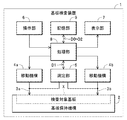
図1に示す基板検査装置1は、「基板検査装置」の一例であって、基板保持機構2、コンタクトプローブ3a,3b、移動機構4a,4b、測定部5、操作部6、表示部7、処理部8および記憶部9を備え、後述する「基板検査方法」に従って検査対象基板Xの良否を電気的に検査可能に構成されている。
A
この場合、検査対象基板Xは「検査対象基板」の一例であって、図2に示すように、導体パターンYa,Ybなどの複数の導体パターン(以下、区別しないときには「導体パターンY」ともいう)が形成されている。また、検査対象基板Xには、隣接する一対の導体パターンY,Y間の絶縁状態や、各導体パターンY毎の導通状態を検査するための複数の「検査ポイント」が規定されている。具体的には、一例として、上記の導体パターンYa,Ybの間の絶縁状態を検査するための「検査ポイント」としては、導体パターンYa上に検査ポイントPaが規定され、導体パターンYb上に検査ポイントPbが規定されているものとする。以下、検査ポイントPa,Pb等を区別しないときには「検査ポイントP」ともいう。 In this case, the inspection target substrate X is an example of the “inspection target substrate”, and as shown in FIG. 2, a plurality of conductor patterns such as the conductor patterns Ya and Yb (hereinafter also referred to as “conductor pattern Y” when not distinguished). ) Is formed. In addition, a plurality of “inspection points” for inspecting an insulation state between a pair of adjacent conductor patterns Y and Y and a conduction state for each conductor pattern Y are defined on the inspection target substrate X. Specifically, as an example, as the “inspection point” for inspecting the insulation state between the conductor patterns Ya and Yb, the inspection point Pa is defined on the conductor pattern Ya, and the inspection is performed on the conductor pattern Yb. It is assumed that the point Pb is defined. Hereinafter, when the inspection points Pa, Pb and the like are not distinguished, they are also referred to as “inspection points P”.
一方、基板保持機構2は、一例として、検査対象基板Xの端部を挟持して所定の検査位置に保持することができるように構成されている。コンタクトプローブ3a,3bは、「一対の検査用プローブ」の一例である伸縮型のピンプローブであって、測定部5に対してそれぞれ電気的に接続されている。移動機構4a,4bは、「移動機構」の一例であって、本例では、移動機構4aが処理部8の制御に従ってコンタクトプローブ3aを任意のXY方向(検査対象基板Xの表面に沿った方向)およびZ方向(検査対象基板Xの表面に垂直な方向)に移動させて任意の検査ポイントPに接触させ、移動機構4bが処理部8の制御に従ってコンタクトプローブ3bを任意のXYZ方向に移動させて任意の検査ポイントPに接触させる構成が採用されている。
On the other hand, the board | substrate holding |
測定部5は、「測定部」の一例であって、後述するように、処理部8の制御に従い、検査対象基板Xに規定された各検査ポイントP,P・・のうちの任意の2箇所にそれぞれ接触させられた両コンタクトプローブ3a,3bを介して両検査ポイントP,Pの間についての各種の電気的パラメータを測定して測定値データD1を出力する測定処理を実行する。なお、測定部5による測定処理については、後に詳細に説明する。
The
操作部6は、基板検査装置1の動作条件の設定操作や、検査処理の開始/停止を指示する操作が可能な操作スイッチを備え、スイッチ操作に応じた操作信号を処理部8に出力する。表示部7は、処理部8の制御に従い、基板検査装置1の動作条件を設定する設定画面、検査対象基板Xについての検査時における動作状態の表示画面、および検査対象基板Xに検査結果などを表示する。
The operation unit 6 includes an operation switch capable of performing an operation condition setting operation of the
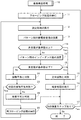
処理部8は、「処理部」の一例であって、基板検査装置1を総括的に制御する。具体的には、処理部8は、図3に示す基板検査処理10を実行して検査対象基板Xの良否を検査し、その検査結果を表示部7に表示させると共に、検査結果データD2を生成して外部装置に出力可能に記憶部9に記憶させる。
The processing unit 8 is an example of a “processing unit”, and comprehensively controls the
より具体的には、処理部8は、両移動機構4a,4bを制御して検査対象基板X上に規定された各検査ポイントP,P・・のうちの一対の検査ポイントP,Pに両コンタクトプローブ3a,3bをそれぞれ接触させる「プロービング処理」を実行する。また、処理部8は、測定部5を制御して測定処理を実行させて「予め規定された検査用被測定量」を測定させると共に、測定処理の測定結果に基づいて両検査ポイントP,Pの間の良否を判別する「検査処理」を実行する。
More specifically, the processing unit 8 controls both the moving
さらに、本例の基板検査装置1における処理部8は、上記の「プロービング処理」の完了後、「検査処理」の開始に先立ち、両コンタクトプローブ3a,3bが接触させられているべき検査ポイントP,Pに正常に接触しているか否かを判別する「確認処理」を実行する構成が採用されている。なお、この「確認処理」については、後に詳細に説明する。
Further, the processing unit 8 in the
記憶部9は、処理部8の動作プログラム、検査対象基板Xについての検査用データD0、測定部5から出力される測定値データD1、および処理部8によって生成される検査結果データD2などを記憶する。
The storage unit 9 stores an operation program of the processing unit 8, inspection data D0 for the inspection target substrate X, measurement value data D1 output from the
次に、基板検査装置1による検査対象基板Xの検査方法について添付図面を参照して説明する。
Next, a method for inspecting the inspection target substrate X by the
なお、検査対象基板Xの良否を検査する際には、前述したように、隣接する一対の導体パターンY,Y間の絶縁状態の検査(絶縁検査)、および各導体パターンY毎の導通状態の検査(導通検査)などの複数種類の検査項目をそれぞれ実行するが、「基板検査装置」および「基板検査方法」についての理解を容易とするために、これらの検査項目のうちの「絶縁検査」の方法(「検査対象基板において相互に絶縁されているべき一対の検査ポイントの間の良否を検査するとき」の一例)について以下に説明する。 In addition, when inspecting the quality of the inspection target substrate X, as described above, the inspection of the insulation state between a pair of adjacent conductor patterns Y and Y (insulation inspection) and the conduction state of each conductor pattern Y are performed. Multiple types of inspection items such as inspection (continuity inspection) are performed, but in order to facilitate understanding of “board inspection device” and “board inspection method”, “insulation inspection” of these inspection items. The method (an example of “inspecting quality between a pair of inspection points that should be insulated from each other on the inspection target substrate”) will be described below.
まず、検査対象基板Xを基板保持機構2によって保持させて検査位置に位置させる。この状態において、操作部6の操作によって検査の開始が指示されたときに、処理部8は、図3に示す基板検査処理10を開始する。
First, the inspection target substrate X is held by the
この基板検査処理10では、処理部8は、まず、検査用データD0に基づいて「プロービング処理」を実行する(ステップ11)。具体的には、一例として、図2に示す導体パターンYa,Yb間の絶縁検査に際して、処理部8は、移動機構4aを制御して導体パターンYaの検査ポイントPaにコンタクトプローブ3aを接触させると共に、移動機構4bを制御して導体パターンYbの検査ポイントPbにコンタクトプローブ3bを接触させる。
In the
次いで、処理部8は、検査用データD0に基づき、「確認処理」を実行する。具体的には、処理部8は、測定部5を制御してコンタクトプローブ3a,3bの間に予め規定された電圧値の交流電圧を印加させた状態において両コンタクトプローブ3a,3bの間を流れる電流の電流値を測定させる(「第1の処理」としての「測定処理」の実行:ステップ12)。これに応じて、測定部5が、測定した電流値を示す測定値データD1を処理部8に出力し、処理部8は、出力された測定値データD1を記憶部9に記憶させる。
Next, the processing unit 8 executes “confirmation processing” based on the inspection data D0. Specifically, the processing unit 8 controls the
続いて、処理部8は、コンタクトプローブ3a,3bの間に印加した交流電圧の電圧値、および上記の測定値データD1に基づき、導体パターンYa,Yb間(検査ポイントPa,Pb)の間の静電容量Cの静電容量値を演算する(「第2の処理」の実行:ステップ13)。 Subsequently, the processing unit 8 determines between the conductor patterns Ya and Yb (inspection points Pa and Pb) based on the voltage value of the AC voltage applied between the contact probes 3a and 3b and the measured value data D1. The capacitance value of the capacitance C is calculated (execution of “second process”: step 13).
この場合、図2に示すように、絶縁検査をすべき導体パターンYa,Ybは、短絡箇所等が生じ得る近接パターンであるため、同図に示すように、両導体パターンYa,Ybの間には静電容量Cが存在する。したがって、両導体パターンYa,Ybが正常に絶縁されている状態(導体パターンYa,Ybの間にインダクタンス成分Lが存在するのと等価の短絡箇所が存在しない状態)において、検査ポイントPa(導体パターンYa)にコンタクトプローブ3aが正常に接触させられ、かつ検査ポイントPb(導体パターンYb)にコンタクトプローブ3bが正常に接触させられているときには、上記の「測定処理」において、静電容量Cの大きさに応じた電流値(以下、「正常時電流値」ともいう)が測定される。
In this case, as shown in FIG. 2, the conductor patterns Ya and Yb to be inspected for insulation are adjacent patterns in which a short-circuited portion or the like may occur. Therefore, as shown in the same figure, between the conductor patterns Ya and Yb, Has a capacitance C. Therefore, in a state where both conductor patterns Ya and Yb are normally insulated (a state where there is no short-circuit portion equivalent to the presence of the inductance component L between the conductor patterns Ya and Yb), the inspection point Pa (conductor pattern Pa When the
したがって、正常に絶縁された両導体パターンYa,Ybの検査ポイントPa,Pbにコンタクトプローブ3a,3bが正常に接触させられているときには、正常時電流値に基づき、検査用データD0に記録されている接触状態判別用の基準値(基準静電容量値:「第1の基準値」の一例)以上の静電容量値が演算される。この際に、処理部8は、静電容量値が基準値以上であると判別し(ステップ14)、両コンタクトプローブ3a,3bが検査ポイントPa,Pbに正常に接触していると判別して「確認処理」を完了し(ステップ15)、検査ポイントPa,Pbの間の絶縁検査を開始する(ステップ16)。 Therefore, when the contact probes 3a and 3b are normally brought into contact with the inspection points Pa and Pb of the normally insulated conductor patterns Ya and Yb, they are recorded in the inspection data D0 based on the normal current value. A capacitance value equal to or greater than the reference value for determining the contact state (reference capacitance value: an example of “first reference value”) is calculated. At this time, the processing unit 8 determines that the capacitance value is greater than or equal to the reference value (step 14), and determines that both the contact probes 3a and 3b are normally in contact with the inspection points Pa and Pb. The “confirmation process” is completed (step 15), and an insulation inspection between the inspection points Pa and Pb is started (step 16).
具体的には、一例として、処理部8は、検査ポイントPa,Pbにコンタクトプローブ3a,3bを接触させた状態を維持しつつ、測定部5を制御して検査ポイントPa,Pb間(導体パターンYa,Yb間)の抵抗値(「予め規定された検査用被測定量」の一例)を測定させる。
Specifically, as an example, the processing unit 8 controls the
また、処理部8は、測定された抵抗値が検査用データD0に記憶されている基準抵抗値以上のときには、検査ポイントPa,Pb間(導体パターンYa,Yb間)が正常に絶縁されていると判別し、良好との判別結果およびその抵抗値を検査ポイントPa,Pbに関連付けて検査結果データD2に記録する。また、処理部8は、測定された抵抗値が検査用データD0に記憶されている基準抵抗値を下回るときには、検査ポイントPa,Pb間(導体パターンYa,Yb間)が正常に絶縁されていないと判別し、不良との判別結果およびその抵抗値を検査ポイントPa,Pbに関連付けて検査結果データD2に記録する。 Further, when the measured resistance value is equal to or higher than the reference resistance value stored in the inspection data D0, the processing unit 8 normally insulates between the inspection points Pa and Pb (between the conductor patterns Ya and Yb). And the result of determination of goodness and its resistance value are recorded in the inspection result data D2 in association with the inspection points Pa and Pb. Further, when the measured resistance value is lower than the reference resistance value stored in the inspection data D0, the processing unit 8 is not normally insulated between the inspection points Pa and Pb (between the conductor patterns Ya and Yb). And the result of determination of failure and its resistance value are recorded in the inspection result data D2 in association with the inspection points Pa and Pb.
続いて、処理部8は、絶縁検査を実行すべき他の検査ステップ(他の検査ポイントP,P)が存在するか否かを判別し(ステップ17)、検査すべき検査ステップが存在するときには、ステップ11に戻り、対象の検査ポイントP,Pに対する「プロービング処理」を実行する。 Subsequently, the processing unit 8 determines whether or not there is another inspection step (other inspection points P and P) to be subjected to the insulation inspection (step 17), and when there is an inspection step to be inspected. Returning to step 11, “probing processing” is performed on the target inspection points P and P.
一方、前述したステップ11の「プロービング処理」において、検査ポイントPa(導体パターンYa)にコンタクトプローブ3aが正常に接触させられ、かつ検査ポイントPb(導体パターンYb)にコンタクトプローブ3bが正常に接触させられていたとしても、図2に示すように、導体パターンYa,Ybの間にインダクタンス成分Lが存在するのと等価の短絡箇所が存在している状態(両導体パターンYa,Ybが正常に絶縁されていない状態)では、ステップ12の「測定処理」において、測定のタイミング(電圧値のサンプリング周期)によっては、正常時電流値よりも小さな値の電流値、または、マイナス値の電流値(以下、「短絡箇所存在時電流値」ともいう)が測定されることがある。
On the other hand, in the “probing process” of
また、導体パターンYa,Yb間の絶縁状態を問わず、前述したステップ11の「プロービング処理」において、コンタクトプローブ3a,3bのいずれか、または双方が検査ポイントPa,Pb(導体パターンYa,Yb)に正常に接触されていないときには、ステップ12の「測定処理」において、正常時電流値よりも小さな値の電流値(以下、「接触不良時電流値」ともいう)が測定される。
In addition, regardless of the insulation state between the conductor patterns Ya and Yb, in the “probing process” in
したがって、両導体パターンYa,Yb間が正常に絶縁されていないときや、コンタクトプローブ3a,3bのいずれか、または双方が検査ポイントPa,Pbに正常に接触していないときには、短絡箇所存在時電流値、または接触不良時電流値に基づき、検査用データD0に記録されている接触状態判別用の基準値を下回る静電容量値が演算される。この際に、処理部8は、静電容量値が基準値を下回ると判別し(ステップ14)、検査ポイントPa,Pb間に印加した交流電圧の電圧値、および記憶部9に記憶させた測定値データD1の値(電流値)に基づき、両検査ポイントPa,Pb間のインピーダンス値を演算する(「第3の処理」の実行:ステップ18)。 Therefore, when the two conductor patterns Ya and Yb are not normally insulated, or when either or both of the contact probes 3a and 3b are not normally in contact with the inspection points Pa and Pb, the current when the short-circuited portion exists Based on the value or the current value at the time of contact failure, a capacitance value lower than the reference value for contact state determination recorded in the inspection data D0 is calculated. At this time, the processing unit 8 determines that the capacitance value is lower than the reference value (step 14), the voltage value of the AC voltage applied between the inspection points Pa and Pb, and the measurement stored in the storage unit 9. Based on the value (current value) of the value data D1, the impedance value between the inspection points Pa and Pb is calculated (execution of “third process”: step 18).
この場合、インダクタンス成分Lが存在するのと等価の短絡箇所が存在する導体パターンYa,Yb(検査ポイントPa,Pbに両コンタクトプローブ3a,3bが正常に接触させられているときには、短絡箇所存在時電流値に基づき、検査用データD0に記録されている接触状態判別用の基準値(基準インピーダンス値:「第2の基準値」の一例)以下のインピーダンス値が演算される。この際に、処理部8は、インピーダンス値が基準値以下であると判別し(ステップ19)、両コンタクトプローブ3a,3bが検査ポイントPa,Pbに正常に接触していると判別して「確認処理」を完了する(ステップ15)。また、処理部8は、前述したステップ16以降の処理を実行する。
In this case, conductor patterns Ya and Yb in which a short-circuit portion equivalent to the presence of the inductance component L exists (when both
一方、導体パターンYa,Yb間の絶縁状態を問わず、前述したステップ11の「プロービング処理」において、コンタクトプローブ3a,3bのいずれか、または双方が検査ポイントPa,Pb(導体パターンYa,Yb)に正常に接触されていないときには、接触不良時電流値に基づき、検査用データD0に記録されている接触状態判別用の基準値(基準インピーダンス値:「第2の基準値」)を超えるインピーダンス値が演算される。この際に、処理部8は、インピーダンス値が基準値を超えると判別し(ステップ19)、両コンタクトプローブ3a,3bが検査ポイントPa,Pbに正常に接触していないと判別して「確認処理」を完了する(ステップ20)。
On the other hand, regardless of the insulation state between the conductor patterns Ya and Yb, in the “probing process” in
この際に、処理部8は、まず、その検査ポイントPa,Pbにコンタクトプローブ3a,3bが正常に接触していないと判別したのが初回であるか否かを判別する(ステップ21)。この場合、本例では、上記のステップ20の判別が検査ポイントPa,Pbに対する初回の判別結果であるため、処理部8は、上記のステップ11に戻り、その検査ポイントPa,Pbにコンタクトプローブ3a,3bを再び接触させる「フロービング処理」を実行する(「第4の処理」としての「再プロービング処理」の実行:ステップ22)。次いで、処理部8は、上記のステップ12以降の各処理を再び実行する。
At this time, the processing unit 8 first determines whether or not it is the first time that it is determined that the contact probes 3a and 3b are not normally in contact with the inspection points Pa and Pb (step 21). In this case, in this example, since the determination in
この場合、例えば、検査ポイントPa,Pbのいずれか、または双方が製造不良等に起因して絶縁膜で覆われた状態となっていたり、検査ポイントPa,Pbのいずれか、または双方にコンタクトプローブ3a,3bの接触を妨げる異物が付着した状態となっていたりしたときには、上記のステップ22の「プロービング処理」を行っても、検査ポイントPa,Pbにコンタクトプローブ3a,3bを正常に接触させることができない。この際に、処理部8は、検査ポイントPa,Pbにコンタクトプローブ3a,3bが正常に接触していないと判別すると共に(ステップ20)、その検査ポイントPa,Pbに対する接触不良との判別が初回ではないと判別する(ステップ21)。
In this case, for example, either or both of the inspection points Pa and Pb are covered with an insulating film due to a manufacturing defect or the like, or the inspection probe Pa or Pb or both are contact probes. When the foreign matter that obstructs the contact between 3a and 3b is attached, the contact probes 3a and 3b are normally brought into contact with the inspection points Pa and Pb even if the “probing process” of
この際に、処理部8は、検査ポイントPa,Pbに対する絶縁検査を実施することができないと判別して(ステップ23)、そのような判別結果を検査結果データD2に記録し、絶縁検査を実行すべき他の検査ステップ(他の検査ポイントP,P)が存在するか否かを判別する(ステップ17)。また、上記の一連の各処理を実行することにより、すべての検査ステップ(絶縁検査を実行すべきすべての検査ポイントP,P)についての検査を終了したときに、処理部8は、この基板検査処理10を終了する。
At this time, the processing unit 8 determines that the insulation inspection for the inspection points Pa and Pb cannot be performed (step 23), records such a determination result in the inspection result data D2, and executes the insulation inspection. It is determined whether there are other inspection steps (other inspection points P, P) to be performed (step 17). In addition, by executing the above-described series of processes, when the inspection for all inspection steps (all inspection points P and P to be subjected to insulation inspection) is completed, the processing unit 8 performs this substrate inspection. The
このように、この基板検査装置1、およびその基板検査方法では、検査対象基板Xにおいて相互に絶縁されているべき一対の検査ポイントP,Pの間の良否を検査するときに、「プロービング処理」を実行して両検査ポイントP,Pに両コンタクトプローブ3a,3bをそれぞれ接触させた後に、両コンタクトプローブ3a,3bの間に予め規定された電圧値の交流電圧を印加させた状態において両コンタクトプローブ3a,3bの間を流れる電流の電流値を測定させる「第1の処理」を実行すると共に、「第1の処理」において測定された電流値に基づいて両検査ポイントP,Pの間の静電容量値を演算する「第2の処理」を実行し、「第2の処理」によって演算した静電容量値が予め規定された「第1の基準値」以上のときには、両検査ポイントP,Pを対象とする「検査処理」を実行すると共に、「第2の処理」によって演算した静電容量値が予め規定された「第1の基準値」を下回るときには、「第1の処理」において測定された電流値に基づいて両検査ポイントP,P間のインピーダンス値を演算する「第3の処理」を実行し、「第3の処理」によって演算したインピーダンス値が予め規定された「第2の基準値」以下のときには、両検査ポイントP,Pを対象とする「検査処理」を実行すると共に、「第3の処理」によって演算したインピーダンス値が予め規定された「第2の基準値」を超えているときには、両コンタクトプローブ3a,3bが両検査ポイントP,Pに正常に接触していないと判別して「検査処理」を実行することなく予め規定された「第4の処理」を実行する。
As described above, in the
したがって、この基板検査装置1、およびその基板検査方法によれば、インダクタンス成分Lが存在するのと等価の短絡箇所が存在する検査ポイントP,Pについて、「検査処理(絶縁検査)」の開始に先立ってコンタクトプローブ3a,3bが正常に接触しているか否かを判別するときに、検査ポイントP,Pにコンタクトプローブ3a,3bが正常に接触しているにも拘わらず、静電容量値に基づいて正常に接触していないと誤って判別されることなく、インピーダンス値に基づいて正常に接触していると正しく判別することができる。これにより、検査対象基板Xの導体パターンYと対向する電極が存在しなくても、検査ポイントP,Pにコンタクトプローブ3a,3bが正常に接触しているか否かを確実に判別し、その検査ポイントP,Pについての「検査処理」を確実に実行することができる。
Therefore, according to this
また、この基板検査装置1、およびその基板検査方法では、両コンタクトプローブ3a,3bが正常に接触していないと判別した両検査ポイントP,Pを対象とする「プロービング処理」を「第4の処理」として実行した後に、「第1の処理」および「第2の処理」を再び実行すると共に、「第2の処理」によって演算した静電容量値に応じて「検査処理」、および「第3の処理」以降の各処理のいずれかを実行する。
In the
したがって、この基板検査装置1、およびその基板検査方法によれば、例えば検査ポイントP,Pとコンタクトプローブ3a,3bとの間に異物が挟まるなどして検査ポイントP,Pにコンタクトプローブ3a,3bが一時的に接触できなかったとしても、「第4の処理」としての「プロービング処理」において、その検査ポイントP,P(または、その検査ポイントP,Pの極く近傍の新たな検査ポイントP,P)に対する「プロービング処理」を実行することで、異物が排除されてコンタクトプローブ3a,3bを正常に接触させることができる。
Therefore, according to the
なお、「基板検査装置」の構成、および「基板検査方法」の内容については、上記の基板検査装置1の構成、および基板検査方法による基板検査処理10の内容の例に限定されない。例えば、ステップ18の「第3の処理」において演算した両検査ポイントPa,Pb間のインピーダンス値が、「第2の基準値」としての接触状態判別用の基準値(基準インピーダンス値)以下のときに(ステップ19)、両コンタクトプローブ3a,3bが検査ポイントPa,Pbに正常に接触していると判別して「確認処理」を完了し(ステップ15)、ステップ16の絶縁検査を実行する構成および方法を例に挙げて説明したが、これに限定されない。例えば、このような構成および方法に代えて、「第3の処理」によって演算したインピーダンス値が「第2の基準値」以下のときに、「検査処理」を実行することなく両検査ポイントP,P間の絶縁状態が不良であると判別して、その検査ポイントP,Pについての検査を終了する構成および方法を採用することもできる。
The configuration of the “substrate inspection apparatus” and the content of the “substrate inspection method” are not limited to the configuration of the
このような構成の「基板検査装置」、およびその「基板検査方法」によれば、インダクタンス成分Lが存在するのと等価の短絡箇所が存在する検査ポイントP,Pについて、「検査処理(絶縁検査)」の開始に先立ってコンタクトプローブ3a,3bが正常に接触しているか否かを判別するときに、検査ポイントP,Pにコンタクトプローブ3a,3bが正常に接触しているにも拘わらず、演算される静電容量値に基づいて正常に接触していないと誤って判別される事態を好適に回避できるだけでなく、絶縁状態が不良であることで低いインピーダンス値が測定される不良の検査ポイントP,Pについての不要な「検査処理」を実行しなくて済む分だけ、検査対象基板Xの検査に要する時間を充分に短縮することができる。 According to the “substrate inspection apparatus” and the “substrate inspection method” having such a configuration, “inspection processing (insulation inspection) is performed on inspection points P and P where there is a short-circuit portion equivalent to the presence of the inductance component L. When the contact probes 3a and 3b are in normal contact prior to the start of ")", the contact probes 3a and 3b are normally in contact with the inspection points P and P, Not only can it avoid the situation that it is mistakenly determined that it is not in normal contact based on the calculated capacitance value, but it also has a defect inspection point where a low impedance value is measured due to a poor insulation state. The time required for the inspection of the inspection target substrate X can be sufficiently shortened by the amount of unnecessary “inspection processing” for P and P.
また、「第4の処理」としての「プロービング処理(再プロービング処理)」において、接触不良が発生していると判別した検査ポイントP,Pにコンタクトプローブ3a,3bを再び接触させる処理を実行する構成および方法を例に挙げて説明したが、このような構成および方法に代えて、接触不良が発生していると判別した検査ポイントP,Pの位置とは僅かに異なる同一パターン上の検査ポイントP,Pにコンタクトプローブ3a,3bを新たに接触させる「プロービング処理(再プロービング処理)」を「第4の処理」として実行する構成および方法を採用することもできる。 Further, in the “probing process (reprobing process)” as the “fourth process”, a process of bringing the contact probes 3a and 3b into contact again with the inspection points P and P determined to have a contact failure is executed. Although the configuration and method have been described by way of example, instead of such a configuration and method, inspection points on the same pattern that are slightly different from the positions of the inspection points P and P that are determined to have poor contact have been described. A configuration and method for executing “probing processing (reprobing processing)” in which the contact probes 3 a and 3 b are newly brought into contact with P and P as “fourth processing” may be employed.
さらに、「第4の処理」は、接触不良が発生していると判別した検査ポイントP,P、または、その検査ポイントP,Pの極く近傍の新たな検査ポイントP,Pにコンタクトプローブ3a,3bを接触させる「プロービング処理」に限定されず、接触不良が発生していると判別した検査ポイントP,Pに接触できないと判別し、他の検査ポイントP,P(他の検査ステップ)についての「プロービング処理」を「第4の処理」として実行する構成および方法を採用することもできる。
Further, the “fourth process” is performed by contacting the
このように、他の検査ポイントP,Pについての「プロービング処理」を「第4の処理」として実行することで、例えば、検査対象基板Xの製造不良に起因して検査ポイントP,Pが絶縁膜で覆われた状態となっており、その検査ポイントP,Pに対する「プロービング処理」を何度実行してもコンタクトプローブ3a,3bを正常に接触させることができないときに、そのような検査ポイントP,Pに対する不要な「プロービング処理」を繰り返すことがない分だけ1枚の検査対象基板Xの検査に要する時間を充分に短縮することができる。 As described above, by performing the “probing process” for the other inspection points P and P as the “fourth process”, for example, the inspection points P and P are insulated due to a manufacturing defect of the inspection target substrate X. Such an inspection point when it is in a state covered with a film and the contact probes 3a and 3b cannot be brought into normal contact no matter how many times the “probing process” is performed on the inspection points P and P. The time required for the inspection of one inspection target substrate X can be sufficiently shortened by the amount that unnecessary “probing processing” for P and P is not repeated.
1 基板検査装置
3a,3b コンタクトプローブ
4a,4b 移動機構
5 測定部
8 処理部
9 記憶部
10 基板検査処理
C 静電容量
D0 検査用データ
D1 測定値データ
D2 検査結果データ
L インダクタンス成分
Pa,Pb 検査ポイント
X 検査対象基板
Ya,Yb 導体パターン
DESCRIPTION OF
Claims (6)
前記両検査用プローブを移動させる移動機構と、
前記両検査用プローブを介して予め規定された検査用被測定量を測定する測定部と、
前記移動機構を制御して前記検査対象基板上の一対の検査ポイントに前記両検査用プローブをそれぞれ接触させるプロービング処理、および前記測定部を制御して前記検査用被測定量を測定させると共に当該測定部による測定結果に基づいて前記一対の検査ポイントの間の良否を判別する検査処理を実行する処理部とを備えた基板検査装置であって、
前記処理部は、前記検査対象基板において相互に絶縁されているべき前記一対の検査ポイントの間の良否を検査するときに、前記プロービング処理を実行して当該両検査ポイントに前記両検査用プローブをそれぞれ接触させた後に、前記測定部を制御して前記両検査用プローブの間に予め規定された電圧値の交流電圧を印加させた状態において当該両検査用プローブの間を流れる電流の電流値を測定させる第1の処理を実行すると共に、当該第1の処理において測定された電流値に基づいて前記両検査ポイントの間の静電容量値を演算する第2の処理を実行し、
前記第2の処理によって演算した静電容量値が予め規定された第1の基準値以上のときには、前記両検査ポイントを対象とする前記検査処理を実行すると共に、前記第2の処理によって演算した静電容量値が前記第1の基準値を下回るときには、前記第1の処理において測定された電流値に基づいて前記両検査ポイント間のインピーダンス値を演算する第3の処理を実行し、
前記第3の処理によって演算したインピーダンス値が予め規定された第2の基準値以下のときには、前記両検査ポイントを対象とする前記検査処理を実行すると共に、前記第3の処理によって演算したインピーダンス値が前記第2の基準値を超えているときには、前記両検査用プローブが前記両検査ポイントに正常に接触していないと判別して前記検査処理を実行することなく予め規定された第4の処理を実行する基板検査装置。 A pair of inspection probes brought into contact with the substrate to be inspected;
A moving mechanism for moving both the inspection probes;
A measuring unit for measuring a predetermined amount to be inspected in advance via both the inspection probes;
Probing processing for controlling the moving mechanism to bring the two inspection probes into contact with a pair of inspection points on the inspection target substrate, and controlling the measurement unit to measure the measurement amount for inspection and the measurement A substrate inspection apparatus including a processing unit that executes an inspection process for determining pass / fail between the pair of inspection points based on a measurement result by the unit,
The processing unit performs the probing process to inspect both the inspection probes at both inspection points when inspecting the quality between the pair of inspection points that should be insulated from each other on the inspection target substrate. After each contact, the current value of the current flowing between the two inspection probes in a state where an AC voltage having a predetermined voltage value is applied between the inspection probes by controlling the measurement unit. Performing a first process to be measured, and executing a second process for calculating a capacitance value between the two inspection points based on the current value measured in the first process,
When the capacitance value calculated by the second process is equal to or greater than a first reference value defined in advance, the inspection process for both the inspection points is executed and the calculation is performed by the second process. When the capacitance value is lower than the first reference value, a third process for calculating an impedance value between the two inspection points based on the current value measured in the first process is executed.
When the impedance value calculated by the third process is equal to or less than a second reference value defined in advance, the impedance process calculated by the third process is performed while performing the test process for both the test points. Is greater than the second reference value, it is determined that the two inspection probes are not normally in contact with the two inspection points, and a fourth process defined in advance without executing the inspection process. Board inspection equipment to perform.
前記両検査用プローブを移動させる移動機構と、
前記両検査用プローブを介して予め規定された検査用被測定量を測定する測定部と、
前記移動機構を制御して前記検査対象基板上の一対の検査ポイントに前記両検査用プローブをそれぞれ接触させるプロービング処理、および前記測定部を制御して前記検査用被測定量を測定させると共に当該測定部による測定結果に基づいて前記一対の検査ポイントの間の良否を判別する検査処理を実行する処理部とを備えた基板検査装置であって、
前記処理部は、前記検査対象基板において相互に絶縁されているべき前記一対の検査ポイントの間の良否を検査するときに、前記プロービング処理を実行して当該両検査ポイントに前記両検査用プローブをそれぞれ接触させた後に、前記測定部を制御して前記両検査用プローブの間に予め規定された電圧値の交流電圧を印加させた状態において当該両検査用プローブの間を流れる電流の電流値を測定させる第1の処理を実行すると共に、当該第1の処理において測定された電流値に基づいて前記両検査ポイントの間の静電容量値を演算する第2の処理を実行し、
前記第2の処理によって演算した静電容量値が予め規定された第1の基準値以上のときには、前記両検査ポイントを対象とする前記検査処理を実行すると共に、前記第2の処理によって演算した静電容量値が前記第1の基準値を下回るときには、前記第1の処理において測定された電流値に基づいて前記両検査ポイント間のインピーダンス値を演算する第3の処理を実行し、
前記第3の処理によって演算したインピーダンス値が予め規定された第2の基準値以下のときには、前記検査処理を実行することなく前記両検査ポイント間の絶縁状態が不良であると判別すると共に、前記第3の処理によって演算したインピーダンス値が前記第2の基準値を超えているときには、前記両検査用プローブが前記両検査ポイントに正常に接触していないと判別して前記検査処理を実行することなく予め規定された第4の処理を実行する基板検査装置。 A pair of inspection probes brought into contact with the substrate to be inspected;
A moving mechanism for moving both the inspection probes;
A measuring unit for measuring a predetermined amount to be inspected in advance via both the inspection probes;
Probing processing for controlling the moving mechanism to bring the two inspection probes into contact with a pair of inspection points on the inspection target substrate, and controlling the measurement unit to measure the measurement amount for inspection and the measurement A substrate inspection apparatus including a processing unit that executes an inspection process for determining pass / fail between the pair of inspection points based on a measurement result by the unit,
The processing unit performs the probing process to inspect both the inspection probes at both inspection points when inspecting the quality between the pair of inspection points that should be insulated from each other on the inspection target substrate. After each contact, the current value of the current flowing between the two inspection probes in a state where an AC voltage having a predetermined voltage value is applied between the inspection probes by controlling the measurement unit. Performing a first process to be measured, and executing a second process for calculating a capacitance value between the two inspection points based on the current value measured in the first process,
When the capacitance value calculated by the second process is equal to or greater than a first reference value defined in advance, the inspection process for both the inspection points is executed and the calculation is performed by the second process. When the capacitance value is lower than the first reference value, a third process for calculating an impedance value between the two inspection points based on the current value measured in the first process is executed.
When the impedance value calculated by the third process is equal to or less than a second reference value defined in advance, it is determined that the insulation state between the two inspection points is defective without performing the inspection process, and When the impedance value calculated by the third process exceeds the second reference value, it is determined that the two inspection probes are not normally in contact with the two inspection points, and the inspection process is executed. A substrate inspection apparatus that executes a predetermined fourth process.
前記検査対象基板において相互に絶縁されているべき前記一対の検査ポイントの間の良否を検査するときに、前記プロービング処理を実行して当該両検査ポイントに前記両検査用プローブをそれぞれ接触させた後に、前記両検査用プローブの間に予め規定された電圧値の交流電圧を印加させた状態において当該両検査用プローブの間を流れる電流の電流値を測定する第1の処理を実行すると共に、当該第1の処理において測定された電流値に基づいて前記両検査ポイントの間の静電容量値を演算する第2の処理を実行し、
前記第2の処理によって演算した静電容量値が予め規定された第1の基準値以上のときには、前記両検査ポイントを対象とする前記検査処理を実行すると共に、前記第2の処理によって演算した静電容量値が前記第1の基準値を下回るときには、前記第1の処理において測定された電流値に基づいて前記両検査ポイント間のインピーダンス値を演算する第3の処理を実行し、
前記第3の処理によって演算したインピーダンス値が予め規定された第2の基準値以下のときには、前記両検査ポイントを対象とする前記検査処理を実行すると共に、前記第3の処理によって演算したインピーダンス値が前記第2の基準値を超えているときには、前記両検査用プローブが前記両検査ポイントに正常に接触していないと判別して前記検査処理を実行することなく予め規定された第4の処理を実行する基板検査方法。 A probing process in which a pair of inspection probes are brought into contact with a pair of inspection points on the inspection target substrate, and a predetermined amount to be measured for inspection specified in advance through the two inspection probes and based on the measurement result A substrate inspection method for performing inspection processing for determining pass / fail between the pair of inspection points,
When inspecting pass / fail between the pair of inspection points that should be insulated from each other on the inspection target substrate, after performing the probing process and bringing the inspection probes into contact with the inspection points, respectively. , Executing a first process for measuring a current value of a current flowing between the two inspection probes in a state where an alternating voltage having a predetermined voltage value is applied between the two inspection probes; Performing a second process of calculating a capacitance value between the two inspection points based on the current value measured in the first process;
When the capacitance value calculated by the second process is equal to or greater than a first reference value defined in advance, the inspection process for both the inspection points is executed and the calculation is performed by the second process. When the capacitance value is lower than the first reference value, a third process for calculating an impedance value between the two inspection points based on the current value measured in the first process is executed.
When the impedance value calculated by the third process is equal to or less than a second reference value defined in advance, the impedance process calculated by the third process is performed while performing the test process for both the test points. Is greater than the second reference value, it is determined that the two inspection probes are not normally in contact with the two inspection points, and a fourth process defined in advance without executing the inspection process. Board inspection method to perform.
前記検査対象基板において相互に絶縁されているべき前記一対の検査ポイントの間の良否を検査するときに、前記プロービング処理を実行して当該両検査ポイントに前記両検査用プローブをそれぞれ接触させた後に、前記両検査用プローブの間に予め規定された電圧値の交流電圧を印加させた状態において当該両検査用プローブの間を流れる電流の電流値を測定する第1の処理を実行すると共に、当該第1の処理において測定された電流値に基づいて前記両検査ポイントの間の静電容量値を演算する第2の処理を実行し、
前記第2の処理によって演算した静電容量値が予め規定された第1の基準値以上のときには、前記両検査ポイントを対象とする前記検査処理を実行すると共に、前記第2の処理によって演算した静電容量値が前記第1の基準値を下回るときには、前記第1の処理において測定された電流値に基づいて前記両検査ポイント間のインピーダンス値を演算する第3の処理を実行し、
前記第3の処理によって演算したインピーダンス値が予め規定された第2の基準値以下のときには、前記検査処理を実行することなく前記両検査ポイント間の絶縁状態が不良であると判別すると共に、前記第3の処理によって演算したインピーダンス値が前記第2の基準値を超えているときには、前記両検査用プローブが前記両検査ポイントに正常に接触していないと判別して前記検査処理を実行することなく予め規定された第4の処理を実行する基板検査方法。 A probing process in which a pair of inspection probes are brought into contact with a pair of inspection points on the inspection target substrate, and a predetermined measurement amount to be inspected in advance through both the inspection probes, and based on the measurement result A substrate inspection method for performing inspection processing for determining pass / fail between the pair of inspection points,
When inspecting pass / fail between the pair of inspection points that should be insulated from each other on the inspection target substrate, after performing the probing process and bringing the inspection probes into contact with the inspection points, respectively. , Executing a first process for measuring a current value of a current flowing between the two inspection probes in a state where an alternating voltage having a predetermined voltage value is applied between the two inspection probes; Performing a second process of calculating a capacitance value between the two inspection points based on the current value measured in the first process;
When the capacitance value calculated by the second process is equal to or greater than a first reference value defined in advance, the inspection process for both the inspection points is executed and the calculation is performed by the second process. When the capacitance value is lower than the first reference value, a third process for calculating an impedance value between the two inspection points based on the current value measured in the first process is executed.
When the impedance value calculated by the third process is equal to or less than a second reference value defined in advance, it is determined that the insulation state between the two inspection points is defective without performing the inspection process, and When the impedance value calculated by the third process exceeds the second reference value, it is determined that the two inspection probes are not normally in contact with the two inspection points, and the inspection process is executed. A substrate inspection method for executing a predetermined fourth process.
Priority Applications (1)
| Application Number | Priority Date | Filing Date | Title |
|---|---|---|---|
| JP2017128224A JP6943648B2 (en) | 2017-06-30 | 2017-06-30 | Board inspection equipment and board inspection method |
Applications Claiming Priority (1)
| Application Number | Priority Date | Filing Date | Title |
|---|---|---|---|
| JP2017128224A JP6943648B2 (en) | 2017-06-30 | 2017-06-30 | Board inspection equipment and board inspection method |
Publications (2)
| Publication Number | Publication Date |
|---|---|
| JP2019012003A true JP2019012003A (en) | 2019-01-24 |
| JP6943648B2 JP6943648B2 (en) | 2021-10-06 |
Family
ID=65226835
Family Applications (1)
| Application Number | Title | Priority Date | Filing Date |
|---|---|---|---|
| JP2017128224A Expired - Fee Related JP6943648B2 (en) | 2017-06-30 | 2017-06-30 | Board inspection equipment and board inspection method |
Country Status (1)
| Country | Link |
|---|---|
| JP (1) | JP6943648B2 (en) |
Cited By (1)
| Publication number | Priority date | Publication date | Assignee | Title |
|---|---|---|---|---|
| WO2024127925A1 (en) * | 2022-12-13 | 2024-06-20 | 日置電機株式会社 | Inspection device, contact status determining device, and contact status determining method |
Citations (5)
| Publication number | Priority date | Publication date | Assignee | Title |
|---|---|---|---|---|
| JP2001242211A (en) * | 2000-02-29 | 2001-09-07 | Hioki Ee Corp | Circuit board inspection equipment |
| JP2001330631A (en) * | 2000-05-24 | 2001-11-30 | Hioki Ee Corp | Circuit board inspection method and circuit board inspection apparatus |
| JP2002014134A (en) * | 2000-06-30 | 2002-01-18 | Hioki Ee Corp | Circuit board inspection equipment |
| JP2016102772A (en) * | 2014-11-29 | 2016-06-02 | 日置電機株式会社 | Circuit board inspection device and circuit board inspection method |
| JP2017101947A (en) * | 2015-11-30 | 2017-06-08 | 日置電機株式会社 | Substrate inspection apparatus and substrate inspection method |
-
2017
- 2017-06-30 JP JP2017128224A patent/JP6943648B2/en not_active Expired - Fee Related
Patent Citations (5)
| Publication number | Priority date | Publication date | Assignee | Title |
|---|---|---|---|---|
| JP2001242211A (en) * | 2000-02-29 | 2001-09-07 | Hioki Ee Corp | Circuit board inspection equipment |
| JP2001330631A (en) * | 2000-05-24 | 2001-11-30 | Hioki Ee Corp | Circuit board inspection method and circuit board inspection apparatus |
| JP2002014134A (en) * | 2000-06-30 | 2002-01-18 | Hioki Ee Corp | Circuit board inspection equipment |
| JP2016102772A (en) * | 2014-11-29 | 2016-06-02 | 日置電機株式会社 | Circuit board inspection device and circuit board inspection method |
| JP2017101947A (en) * | 2015-11-30 | 2017-06-08 | 日置電機株式会社 | Substrate inspection apparatus and substrate inspection method |
Cited By (1)
| Publication number | Priority date | Publication date | Assignee | Title |
|---|---|---|---|---|
| WO2024127925A1 (en) * | 2022-12-13 | 2024-06-20 | 日置電機株式会社 | Inspection device, contact status determining device, and contact status determining method |
Also Published As
| Publication number | Publication date |
|---|---|
| JP6943648B2 (en) | 2021-10-06 |
Similar Documents
| Publication | Publication Date | Title |
|---|---|---|
| WO2018159190A1 (en) | Inspection system and malfunction analysis/prediction method for inspection system | |
| JP5507430B2 (en) | Circuit board inspection equipment | |
| JP2008203077A (en) | Circuit inspection device and method | |
| JP2010032457A (en) | Insulation inspecting apparatus and technique | |
| JP5507363B2 (en) | Circuit board inspection apparatus and circuit board inspection method | |
| JP4582869B2 (en) | Circuit board inspection equipment | |
| JP6943648B2 (en) | Board inspection equipment and board inspection method | |
| JP5875815B2 (en) | Circuit board inspection apparatus and circuit board inspection method | |
| JP5317554B2 (en) | Circuit board inspection apparatus and circuit board inspection method | |
| JP6949675B2 (en) | Processing equipment, inspection equipment and processing method | |
| JP4987497B2 (en) | Circuit board inspection equipment | |
| JP5415134B2 (en) | Inspection apparatus and inspection method | |
| JP6918659B2 (en) | Circuit board inspection equipment | |
| JP2001235505A (en) | Circuit board inspection equipment | |
| JP2009288115A (en) | Inspection device and inspection method | |
| JP5485012B2 (en) | Circuit board inspection apparatus and circuit board inspection method | |
| JP6999327B2 (en) | Board inspection equipment | |
| JP5420303B2 (en) | Circuit board inspection apparatus and circuit board inspection method | |
| JP2014020815A (en) | Substrate inspection device and substrate inspection method | |
| JP5988557B2 (en) | Circuit board inspection apparatus and circuit board inspection method | |
| CN112444676A (en) | Resistance detection method and device, resistance detector and readable storage medium | |
| JP2006071567A (en) | Probe contact state determination method, circuit board inspection method, and circuit board inspection apparatus | |
| JP4369002B2 (en) | Circuit board inspection equipment | |
| JP5323502B2 (en) | Substrate inspection apparatus and substrate inspection method | |
| JP4597236B2 (en) | Circuit board inspection method and circuit board inspection apparatus |
Legal Events
| Date | Code | Title | Description |
|---|---|---|---|
| A621 | Written request for application examination |
Free format text: JAPANESE INTERMEDIATE CODE: A621 Effective date: 20200420 |
|
| A977 | Report on retrieval |
Free format text: JAPANESE INTERMEDIATE CODE: A971007 Effective date: 20210208 |
|
| A131 | Notification of reasons for refusal |
Free format text: JAPANESE INTERMEDIATE CODE: A131 Effective date: 20210216 |
|
| A521 | Request for written amendment filed |
Free format text: JAPANESE INTERMEDIATE CODE: A523 Effective date: 20210304 |
|
| TRDD | Decision of grant or rejection written | ||
| A01 | Written decision to grant a patent or to grant a registration (utility model) |
Free format text: JAPANESE INTERMEDIATE CODE: A01 Effective date: 20210824 |
|
| A61 | First payment of annual fees (during grant procedure) |
Free format text: JAPANESE INTERMEDIATE CODE: A61 Effective date: 20210909 |
|
| R150 | Certificate of patent or registration of utility model |
Ref document number: 6943648 Country of ref document: JP Free format text: JAPANESE INTERMEDIATE CODE: R150 |
|
| LAPS | Cancellation because of no payment of annual fees |