JP2019014165A - Light irradiation device - Google Patents
Light irradiation device Download PDFInfo
- Publication number
- JP2019014165A JP2019014165A JP2017133882A JP2017133882A JP2019014165A JP 2019014165 A JP2019014165 A JP 2019014165A JP 2017133882 A JP2017133882 A JP 2017133882A JP 2017133882 A JP2017133882 A JP 2017133882A JP 2019014165 A JP2019014165 A JP 2019014165A
- Authority
- JP
- Japan
- Prior art keywords
- light
- irradiation
- ultraviolet light
- horizontal axis
- axis direction
- Prior art date
- Legal status (The legal status is an assumption and is not a legal conclusion. Google has not performed a legal analysis and makes no representation as to the accuracy of the status listed.)
- Granted
Links
Images



Classifications
-
- B—PERFORMING OPERATIONS; TRANSPORTING
- B41—PRINTING; LINING MACHINES; TYPEWRITERS; STAMPS
- B41J—TYPEWRITERS; SELECTIVE PRINTING MECHANISMS, i.e. MECHANISMS PRINTING OTHERWISE THAN FROM A FORME; CORRECTION OF TYPOGRAPHICAL ERRORS
- B41J2/00—Typewriters or selective printing mechanisms characterised by the printing or marking process for which they are designed
- B41J2/435—Typewriters or selective printing mechanisms characterised by the printing or marking process for which they are designed characterised by selective application of radiation to a printing material or impression-transfer material
- B41J2/447—Typewriters or selective printing mechanisms characterised by the printing or marking process for which they are designed characterised by selective application of radiation to a printing material or impression-transfer material using arrays of radiation sources
- B41J2/45—Typewriters or selective printing mechanisms characterised by the printing or marking process for which they are designed characterised by selective application of radiation to a printing material or impression-transfer material using arrays of radiation sources using light-emitting diode [LED] or laser arrays
- B41J2/451—Special optical means therefor, e.g. lenses, mirrors, focusing means
-
- B—PERFORMING OPERATIONS; TRANSPORTING
- B41—PRINTING; LINING MACHINES; TYPEWRITERS; STAMPS
- B41J—TYPEWRITERS; SELECTIVE PRINTING MECHANISMS, i.e. MECHANISMS PRINTING OTHERWISE THAN FROM A FORME; CORRECTION OF TYPOGRAPHICAL ERRORS
- B41J11/00—Devices or arrangements of selective printing mechanisms, e.g. ink-jet printers or thermal printers, for supporting or handling copy material in sheet or web form
- B41J11/0015—Devices or arrangements of selective printing mechanisms, e.g. ink-jet printers or thermal printers, for supporting or handling copy material in sheet or web form for treating before, during or after printing or for uniform coating or laminating the copy material before or after printing
- B41J11/002—Curing or drying the ink on the copy materials, e.g. by heating or irradiating
- B41J11/0021—Curing or drying the ink on the copy materials, e.g. by heating or irradiating using irradiation
- B41J11/00214—Curing or drying the ink on the copy materials, e.g. by heating or irradiating using irradiation using UV radiation
-
- B—PERFORMING OPERATIONS; TRANSPORTING
- B41—PRINTING; LINING MACHINES; TYPEWRITERS; STAMPS
- B41F—PRINTING MACHINES OR PRESSES
- B41F23/00—Devices for treating the surfaces of sheets, webs, or other articles in connection with printing
- B41F23/04—Devices for treating the surfaces of sheets, webs, or other articles in connection with printing by heat drying, by cooling, by applying powders
-
- B—PERFORMING OPERATIONS; TRANSPORTING
- B41—PRINTING; LINING MACHINES; TYPEWRITERS; STAMPS
- B41F—PRINTING MACHINES OR PRESSES
- B41F23/00—Devices for treating the surfaces of sheets, webs, or other articles in connection with printing
- B41F23/04—Devices for treating the surfaces of sheets, webs, or other articles in connection with printing by heat drying, by cooling, by applying powders
- B41F23/0403—Drying webs
- B41F23/0406—Drying webs by radiation
- B41F23/0409—Ultraviolet dryers
-
- B—PERFORMING OPERATIONS; TRANSPORTING
- B41—PRINTING; LINING MACHINES; TYPEWRITERS; STAMPS
- B41F—PRINTING MACHINES OR PRESSES
- B41F23/00—Devices for treating the surfaces of sheets, webs, or other articles in connection with printing
- B41F23/04—Devices for treating the surfaces of sheets, webs, or other articles in connection with printing by heat drying, by cooling, by applying powders
- B41F23/044—Drying sheets, e.g. between two printing stations
- B41F23/045—Drying sheets, e.g. between two printing stations by radiation
- B41F23/0453—Drying sheets, e.g. between two printing stations by radiation by ultraviolet dryers
-
- B—PERFORMING OPERATIONS; TRANSPORTING
- B41—PRINTING; LINING MACHINES; TYPEWRITERS; STAMPS
- B41M—PRINTING, DUPLICATING, MARKING, OR COPYING PROCESSES; COLOUR PRINTING
- B41M5/00—Duplicating or marking methods; Sheet materials for use therein
- B41M5/0011—Pre-treatment or treatment during printing of the recording material, e.g. heating, irradiating
-
- F—MECHANICAL ENGINEERING; LIGHTING; HEATING; WEAPONS; BLASTING
- F21—LIGHTING
- F21V—FUNCTIONAL FEATURES OR DETAILS OF LIGHTING DEVICES OR SYSTEMS THEREOF; STRUCTURAL COMBINATIONS OF LIGHTING DEVICES WITH OTHER ARTICLES, NOT OTHERWISE PROVIDED FOR
- F21V5/00—Refractors for light sources
- F21V5/04—Refractors for light sources of lens shape
-
- F—MECHANICAL ENGINEERING; LIGHTING; HEATING; WEAPONS; BLASTING
- F21—LIGHTING
- F21V—FUNCTIONAL FEATURES OR DETAILS OF LIGHTING DEVICES OR SYSTEMS THEREOF; STRUCTURAL COMBINATIONS OF LIGHTING DEVICES WITH OTHER ARTICLES, NOT OTHERWISE PROVIDED FOR
- F21V7/00—Reflectors for light sources
- F21V7/005—Reflectors for light sources with an elongated shape to cooperate with linear light sources
-
- F—MECHANICAL ENGINEERING; LIGHTING; HEATING; WEAPONS; BLASTING
- F21—LIGHTING
- F21V—FUNCTIONAL FEATURES OR DETAILS OF LIGHTING DEVICES OR SYSTEMS THEREOF; STRUCTURAL COMBINATIONS OF LIGHTING DEVICES WITH OTHER ARTICLES, NOT OTHERWISE PROVIDED FOR
- F21V7/00—Reflectors for light sources
- F21V7/04—Optical design
- F21V7/06—Optical design with parabolic curvature
-
- F—MECHANICAL ENGINEERING; LIGHTING; HEATING; WEAPONS; BLASTING
- F21—LIGHTING
- F21Y—INDEXING SCHEME ASSOCIATED WITH SUBCLASSES F21K, F21L, F21S and F21V, RELATING TO THE FORM OR THE KIND OF THE LIGHT SOURCES OR OF THE COLOUR OF THE LIGHT EMITTED
- F21Y2103/00—Elongate light sources, e.g. fluorescent tubes
- F21Y2103/10—Elongate light sources, e.g. fluorescent tubes comprising a linear array of point-like light-generating elements
-
- F—MECHANICAL ENGINEERING; LIGHTING; HEATING; WEAPONS; BLASTING
- F21—LIGHTING
- F21Y—INDEXING SCHEME ASSOCIATED WITH SUBCLASSES F21K, F21L, F21S and F21V, RELATING TO THE FORM OR THE KIND OF THE LIGHT SOURCES OR OF THE COLOUR OF THE LIGHT EMITTED
- F21Y2115/00—Light-generating elements of semiconductor light sources
- F21Y2115/10—Light-emitting diodes [LED]
-
- G—PHYSICS
- G02—OPTICS
- G02B—OPTICAL ELEMENTS, SYSTEMS OR APPARATUS
- G02B3/00—Simple or compound lenses
- G02B2003/0093—Simple or compound lenses characterised by the shape
Landscapes
- Engineering & Computer Science (AREA)
- Health & Medical Sciences (AREA)
- General Health & Medical Sciences (AREA)
- Toxicology (AREA)
- Mechanical Engineering (AREA)
- General Engineering & Computer Science (AREA)
- Physics & Mathematics (AREA)
- Optics & Photonics (AREA)
- Led Device Packages (AREA)
- Supply, Installation And Extraction Of Printed Sheets Or Plates (AREA)
- Optical Elements Other Than Lenses (AREA)
- Non-Portable Lighting Devices Or Systems Thereof (AREA)
- Coating Apparatus (AREA)
Abstract
【課題】所定のワーキングディスタンス内において、所定の照射強度及び照射強度分布を有するライン状の光を照射可能な光照射装置を提供すること。【解決手段】基準の照射面上の所定の照射位置に、第1方向に延び、且つ、第1方向と直交する第2方向に所定の線幅を有するライン状の光を照射する光照射装置が、基板と、基板上に第1方向に沿って所定間隔毎に並べられ、第1方向及び第2方向と直交する第3方向に光軸の向きを揃えて配置された複数の光源と、を有する発光ユニットと、該発光ユニットから照射された光を反射させて集光するミラー面を有するミラー部と、を備え、ミラー部を第2方向と第3方向とで規定される平面に沿って切断した断面において、ミラー面の断面形状が、第2方向を横軸x、第3方向を縦軸yとする座標における放物線y=ax2(aは、係数)の横軸方向正側の部分及び横軸方向負側の部分を、それぞれ原点を中心に前記縦軸に向かって同じ回転角度で回転させた曲線形状をなしている。【選択図】図3To provide a light irradiation apparatus capable of irradiating line-shaped light having a predetermined irradiation intensity and irradiation intensity distribution within a predetermined working distance. A light irradiation apparatus that irradiates a line-shaped light that extends in a first direction and has a predetermined line width in a second direction orthogonal to the first direction to a predetermined irradiation position on a reference irradiation surface. Are arranged at predetermined intervals along the first direction on the substrate, and a plurality of light sources arranged with the direction of the optical axis aligned in a third direction orthogonal to the first direction and the second direction, And a mirror part having a mirror surface that reflects and collects the light emitted from the light emitting unit, and the mirror part is along a plane defined by the second direction and the third direction. The cross-sectional shape of the mirror surface is a portion on the positive side in the horizontal axis direction of a parabola y = ax2 (a is a coefficient) at a coordinate having the second direction as the horizontal axis x and the third direction as the vertical axis y. And the part on the negative side in the horizontal axis direction, the same rotation from the origin to the vertical axis. It forms a curved shape that is rotated by an angle. [Selection] Figure 3
Description
本発明は、ライン状の照射光を照射する光照射装置に関する。 The present invention relates to a light irradiation apparatus that emits linear irradiation light.
従来、紫外光の照射により硬化するインクを紙などの印刷対象物に転写させて印刷する印刷機が知られている。このような印刷機は、印刷対象物上のインクを硬化させるために紫外光照射装置を備えている。そして、このような紫外光照射装置においては、低消費電力化や長寿命化の要求から、従来の放電ランプに替えて、LED(Light Emitting Diode)を光源として利用した構成が提案されている(例えば、特許文献1)。 2. Description of the Related Art Conventionally, printing machines that perform printing by transferring ink that is cured by irradiation with ultraviolet light onto a printing object such as paper are known. Such a printing machine includes an ultraviolet light irradiation device in order to cure the ink on the printing object. And in such an ultraviolet light irradiation apparatus, the structure using LED (Light Emitting Diode) as a light source is proposed instead of the conventional discharge lamp from the request | requirement of low power consumption and long lifetime ( For example, Patent Document 1).
特許文献1に記載の発光装置は、複数の発光素子が長手方向に一定間隔に並べられ、ライン状の光を出射する光源部と、光源部に対向する側に反射面を有し、光源部からの光を反射する反射部とを備えている。反射面は、光源部の延長方向に対し直交する断面形状が放物線であり、光源部からの光を平行光として発光装置から出射するように構成されている。
The light-emitting device described in
特許文献1に記載の発光装置によれば、印刷対象物上の所定位置で紫外光の照射強度を向上させることができ、照射強度分布を均一化させることができる。しかしながら、紫外光照射装置が搭載される印刷機(例えば、オフセット枚葉印刷機)においては、紫外光照射の対象となる印刷対象物が変形しやすい紙である場合が多く、搬送中に紙がばたつくことも多い。このように印刷対象物が変形すると、印刷対象物上で所望の照射強度及び照射強度分布が得られず、インクの硬化状態にむらができるといった問題がある。
According to the light emitting device described in
本発明は、このような事情に鑑みてなされたものであり、その目的とするところは、所定のワーキングディスタンス内において、所定の照射強度及び照射強度分布を有するライン状の光を照射可能な光照射装置を提供することである。 The present invention has been made in view of such circumstances, and an object of the present invention is light capable of irradiating linear light having a predetermined irradiation intensity and irradiation intensity distribution within a predetermined working distance. It is to provide an irradiation apparatus.
上記目的を達成するため、本発明の光照射装置は、基準の照射面上の所定の照射位置に、第1方向に延び、且つ、前記第1方向と直交する第2方向に所定の線幅を有するライン状の光を照射する光照射装置であって、基板と、基板上に第1方向に沿って所定間隔毎に並べられ、第1方向及び第2方向と直交する第3方向に光軸の向きを揃えて配置された複数の光源と、を有する発光ユニットと、発光ユニットから照射された光を反射させて集光するミラー面を有するミラー部と、を備え、ミラー部を第2方向と第3方向とで規定される平面に沿って切断した断面において、ミラー面の断面形状が、第2方向を横軸x、第3方向を縦軸yとする座標における放物線y=ax2(aは、係数)の横軸方向正側の部分及び横軸方向負側の部分を、それぞれ原点を中心に縦軸に向かって同じ回転角度θで回転させた曲線形状をなしていることを特徴とする。 In order to achieve the above object, a light irradiation apparatus according to the present invention has a predetermined line width in a second direction extending in a first direction and perpendicular to the first direction at a predetermined irradiation position on a reference irradiation surface. A light irradiating apparatus for irradiating a line-shaped light having a light beam in a third direction arranged on the substrate at predetermined intervals along the first direction and orthogonal to the first direction and the second direction. A light emitting unit having a plurality of light sources arranged with their axes aligned, and a mirror part having a mirror surface that reflects and collects the light emitted from the light emitting unit. In a cross section cut along a plane defined by the direction and the third direction, the cross-sectional shape of the mirror surface is a parabola y = ax 2 at coordinates where the second direction is the horizontal axis x and the third direction is the vertical axis y. (A is a coefficient) The portion on the positive side in the horizontal axis direction and the portion on the negative side in the horizontal axis direction Respectively origin curvilinear shape is rotated at the same rotation angle θ toward the vertical axis around the wherein the are.
このような構成によれば、照射面に対して垂直な方向の所定の範囲内において、発光ユニットから出射される紫外光を集光させることができるため、所定の範囲内(所定のワーキングディスタンス内)において所望する照射強度及び照射強度分布が得られる。 According to such a configuration, the ultraviolet light emitted from the light emitting unit can be condensed within a predetermined range in a direction perpendicular to the irradiation surface, and therefore within a predetermined range (within a predetermined working distance). ), The desired irradiation intensity and irradiation intensity distribution are obtained.
また、放物線の係数aが1〜3であることが望ましい。 Moreover, it is desirable that the coefficient a of the parabola is 1 to 3.
また、回転角度θは、3〜10°であることが望ましい。 In addition, the rotation angle θ is preferably 3 to 10 °.
また、曲線形状は、さらに、回転後の放物線の横軸方向正側の部分及び横軸方向負側の部分のそれぞれを横軸に沿って縦軸側に移動させた形状であることが望ましい。 Further, it is desirable that the curved shape is a shape obtained by moving each of the part on the positive side in the horizontal axis direction and the part on the negative side in the horizontal axis direction of the parabola after rotation to the vertical axis side along the horizontal axis.
また、回転後の放物線の横軸正側の部分及び横軸負側の部分のそれぞれの縦軸側への移動距離は、0.5〜4mmであることが望ましい。 Moreover, it is preferable that the moving distance to the vertical axis side of the part on the horizontal axis positive side and the part on the negative side of the horizontal axis of the parabola after rotation is 0.5 to 4 mm.
また、光源は、原点から縦軸正側にオフセットした位置に配置されていることが望ましい。 Further, it is desirable that the light source is disposed at a position offset from the origin to the positive side of the vertical axis.
また、光源の原点からのオフセット量は、3〜7mmであることが望ましい。 The offset amount from the light source origin is preferably 3 to 7 mm.
また、発光ユニットは、各光源を覆うように基板上に配置された封止レンズを有することが望ましい。 In addition, the light emitting unit desirably includes a sealing lens disposed on the substrate so as to cover each light source.
また、光が、紫外線硬化樹脂に作用する波長の光であることが望ましい。 Further, it is desirable that the light has a wavelength that acts on the ultraviolet curable resin.
以上のように、本発明の光照射装置によれば、所定のワーキングディスタンス内において、所定の照射強度及び照射強度分布を有するライン状の光を照射することが可能となる。 As described above, according to the light irradiation apparatus of the present invention, it is possible to irradiate linear light having a predetermined irradiation intensity and irradiation intensity distribution within a predetermined working distance.
以下、本発明の実施の形態について図面を参照して詳細に説明する。なお、図中同一又は相当部分には同一の符号を付してその説明は繰り返さない。 Hereinafter, embodiments of the present invention will be described in detail with reference to the drawings. In addition, the same code | symbol is attached | subjected to the same or an equivalent part in a figure, and the description is not repeated.
(第1実施形態)
まず、本発明の光照射装置の第1実施形態について説明する。図1は、本発明の第1実施形態に係る光照射装置1の外観図である。本実施形態の光照射装置1は、紫外光により硬化するインクを紙などの印刷対象物に転写させて印刷する印刷機(不図示)に搭載される装置であり、後述するように印刷対象物に対向して配置され、印刷対象物に対してライン状の紫外光を出射する(図4(a))。本明細書においては、光照射装置1から出射されるライン状の紫外光の長手(線長)方向をX軸方向(第1方向)、短手(線幅)方向をY軸方向(第2方向)、X軸及びY軸と直交する方向をZ軸方向(第3方向)と定義して説明する。図1(a)は、Y軸方向から見たときの光照射装置1の正面図である。図1(b)は、Z軸方向から見たとき(図1(a)の下側から上側に見たとき)の光照射装置1の底面図である。図1(c)は、X軸方向から見たとき(図1(a)の右側から左側に見たとき)の光照射装置1の側面図である。
(First embodiment)
First, a first embodiment of the light irradiation apparatus of the present invention will be described. FIG. 1 is an external view of a
図1に示すように、光照射装置1は、ケース10、基台ブロック20、ミラー部30及びLEDユニット100を備えている。ケース10は、基台ブロック20、ミラー部30及びLEDユニット100(発光ユニット)を収容するケース(筐体)であり、下面(光照射装置1の下面)に開口する開口部10aを有している。また、LEDユニット100は、X軸方向に平行なライン状の紫外光を出射するユニットである(詳細は後述)。
As shown in FIG. 1, the
基台ブロック20は、LEDユニット100を固定するための支持部材であり、ステンレス鋼等の金属によって形成されている。図1(b)及び(c)に示すように、基台ブロック20は、X軸方向に延びる略矩形の板状の部材である。基台ブロック20の下面の幅方向(Y軸方向)の中央部には、X軸方向に延びるLEDユニット100が配置され、ネジ止めやハンダ付け等によって固着されている。
The
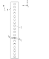
図2は、第1実施形態のLEDユニット100の構成を説明する図であり、LEDユニット100をZ軸方向から見たときの図である。図2に示すように、LEDユニット100は、X軸方向に延びる矩形状の基板101と、基板101上にX軸方向に沿って所定間隔毎に配置された120個のLED(Light Emitting Diode)素子111(光源)とを備えている。複数のLED素子111は、Z軸方向に光軸の向きを揃えて配置され、基板101と電気的に接続されている。LEDユニット100の基板101は、不図示の印刷機のLED駆動回路に接続されており、各LED素子111には、基板101を介してLED駆動回路からの駆動電流が供給されるようになっている。各LED素子111は、略正方形の発光面を備え、LED駆動回路から駆動電流の供給を受けて、インクの硬化波長(例えば、365nm、385nm、395nm、405nm)の紫外光を出射する。その結果、LEDユニット100からはX軸に平行なライン状の紫外光が出射される。なお、本実施形態の各LED素子111は、略一様な光量の紫外光を出射するように各LED素子111に供給される駆動電流が調整されており、LEDユニット100から出射されるライン状の紫外光は、X軸方向において略均一な照射強度分布を有している(詳細は後述)。なお、図2においては、LED素子111は、1つのチップ(ダイス)を有するものとして示しているが、例えば、2個(X軸方向)×2個(Y軸方向)の態様で複数のチップを有するものを使用することもできる。
FIG. 2 is a diagram illustrating the configuration of the
また、基板101上には、LED素子111を囲むミラー面301を有するミラー部30が配置されている。ミラー部30には、X軸方向に沿って延び、且つ、Z軸方向に貫通する貫通孔31が形成されている。貫通孔31の上側(基台ブロック20側)の開口において、LED素子111が貫通孔31に露出し、貫通孔31の下側の開口がケース10の開口部10aと連通している。また、貫通孔31の開口面積は、上側から下側に向かって漸増しており、ミラー部30の貫通孔31を規定する内面がミラー面301を構成している。ミラー面301は、ミラー部30をアルミニウム等の金属で形成することや、ミラー部30の貫通孔31を規定する内面に光反射性薄膜を設けることにより形成することができる。LEDユニット100から出射された紫外光は、ミラー面301で反射された後、集光されつつ、開口部10aを通って印刷対象物に向かって出射するように構成されている。なお、本実施形態では、貫通孔31のX軸方向両端は、ケース10の壁面によって覆われているが、開放されていてもよい。
On the
本発明では、ミラー面301が所定の断面形状を有することに特徴を有する。図3は、第1実施形態のミラー面301の断面形状の特徴を説明する図である。また、図4は、第1実施形態の光照射装置1から出射される紫外光の光線を説明する光線図であり、図4(a)は第1実施形態の光照射装置1から出射される紫外光の光線図であり、図4(b)は比較例の光照射装置1Aから出射される紫外光の光線図である。なお、図4(a)において、「R」は印刷対象物が搬送される基準の照射面を示し、一点鎖線は、LEDユニット100の光軸AXを示している。また、「F1」は、光軸AXが交差する照射面R上の基準の照射位置であり、「LW」は、基準の照射位置F1における紫外光の線幅を示している。
The present invention is characterized in that the
図3に示すように、ミラー部30をY軸方向(第2方向)とZ軸方向(第3方向)とによって規定される平面に沿って切断した断面において、ミラー面301の断面形状が、Y軸方向(第2方向)を横軸x、Z軸方向(第3方向)を縦軸yとする座標における基準の放物線P(y=ax2)の横軸方向正側の部分及び横軸方向負側の部分を、それぞれ原点Oを中心に縦軸に向かって同じ回転角度θで回転させたような曲線形状をなしている。ミラー面301の断面形状がこのような曲線形状であることにより、図4(a)に示すように、LEDユニット100から出射された紫外光は、ミラー面301で反射された後、集光されつつ照射面R上に照射される。紫外光を照射面上に集光させることにより、線幅LWの領域における紫外光のY軸方向の照射強度を、インクの硬化に必要な所定値(本実施形態では、約2W/cm2)以上に設定することができる。
As shown in FIG. 3, the cross-sectional shape of the
これに対して、ミラー面301の断面形状が基準の放物線Pに沿った曲線形状(つまり、放物線形状)をなしていると、図4(b)に示すように、LEDユニット100から出射された紫外光は、ミラー面301で反射された後、集光されることなくほぼ平行光として照射面R上に照射される。このため、比較例の構成では、高強度の紫外光を出射する高価なLED素子111を用いない限り、Y軸方向の照射強度をインクの硬化に必要な所定値以上に設定することが困難である。
On the other hand, when the cross-sectional shape of the
線幅LWは、例えば放物線Pの形状、放物線Pの原点Oを中心とする回転角度θ等を設定することにより調整することができる。具体的には、放物線Pの方程式:y=ax2において、係数aが1〜3程度であることが好ましく、1.5〜2.5程度であることがより好ましい。また、回転角度θは、3〜10°程度であることが好ましく、6〜8°程度であることがより好ましい。このようにして調整される線幅LWは、10〜30mm程度(つまり、基準の照射位置F1に対して±5〜15mm程度の範囲)であることが好ましく、15〜25mm程度であることがより好ましく、本実施形態では、約20mmに設定されている。また、線長LLの領域は、紫外線のX軸方向の照射強度が、インクの硬化に必要な所定値(本実施形態では、約2W/cm2)以上の領域である。また、線長LLは、印刷対象物のサイズに応じて適宜設定されるが、本実施形態においては、約600mmに設定されている。 The line width LW can be adjusted, for example, by setting the shape of the parabola P, the rotation angle θ about the origin O of the parabola P, and the like. Specifically, in the parabola P equation: y = ax 2 , the coefficient a is preferably about 1 to 3, and more preferably about 1.5 to 2.5. The rotation angle θ is preferably about 3 to 10 °, and more preferably about 6 to 8 °. The line width LW adjusted in this way is preferably about 10 to 30 mm (that is, a range of about ± 5 to 15 mm with respect to the reference irradiation position F1), and more preferably about 15 to 25 mm. Preferably, in this embodiment, it is set to about 20 mm. Further, the region of the line length LL is a region where the irradiation intensity in the X-axis direction of ultraviolet rays is equal to or more than a predetermined value (about 2 W / cm 2 in this embodiment) necessary for ink curing. In addition, the line length LL is appropriately set according to the size of the print object, but is set to about 600 mm in the present embodiment.
また、ミラー面301の断面形状を前記のような曲線形状とすることにより、各LED素子111から出射される紫外光の一部がインクの硬化に寄与しない方向へ漏れ出る可能性を低減して、紫外光の照射強度の向上を図ることができる。かかる観点から、各LED素子111は、放物線P(y=ax2)の原点Oから縦軸正側(つまり、Z軸方向)にオフセットした位置に配置されていることが好ましい。この場合、各LED素子111の原点Oからのオフセット量(図3中、「S」で示す)は、3〜7mm程度であることが好ましく、4〜6mm程度であることがより好ましい。このように、各LED素子111を原点OからZ軸正側にズレた位置に配置することにより、各LED素子111から出射される紫外光の大部分を効率よく取り出すことができる。
Further, by making the cross-sectional shape of the mirror surface 301 a curved shape as described above, it is possible to reduce the possibility that part of the ultraviolet light emitted from each
また、本実施形態の光照射装置1においては、ケース10の端からZ軸方向に120mm離れた位置(図4中、「WD120」と示す)におけるX−Y平面を基準の照射面Rとし、印刷対象物は、不図示の印刷機の搬送装置によって基準の照射面R上をY軸方向に沿って搬送されるように構成されている。従って、印刷対象物が基準の照射面R上を順次搬送されることにより、LEDユニット100から出射される紫外光が印刷対象物上を順次移動(走査)し、印刷対象物上のインクを順次硬化(定着)させる。なお、本明細書においては、ケース10の端を基準としたZ軸方向の距離を光照射装置1のワーキングディスタンス(WD)といい、以下、例えば、ワーキングディスタンス120mmの位置を「WD120」という。
Further, in the
上述したように、LEDユニット100から出射されるライン状の紫外光を印刷対象物上に集光させることによって印刷対象物上のインクを定着させることができる。ここで、インクを定着させるために必要な紫外光の照射強度の観点からは、ライン状の紫外光を印刷対象物上の所定の範囲内に集光させることが望ましい。しかし、紫外光照射の対象となる印刷対象物は、紙である場合も多く、搬送中にばたつく(すなわち、Z軸方向の位置が変動する)ことも多い。このように印刷対象物の位置がZ軸方向に変動すると(すなわち、印刷対象物が基準の照射面R上を通過しないと)、ライン状の紫外光が所定のワーキングディスタンスとは異なる位置で印刷対象物上に入射することとなり、所定の照射強度の紫外光を印刷対象物上に照射できなくなるといった問題が生じる。そして、紫外光の照射強度が、インクを定着させるために必要な照射強度に達しないと、インクの硬化状態にむらができるといった問題が発生する。そこで、本発明者は鋭意検討した結果、ミラー面301の断面形状を所定の曲線形状とし(つまり、放物線P(y=ax2)の横軸方向正側の部分及び横軸方向負側の部分を、それぞれ原点Oを中心に縦軸に向かって同じ回転角度θで回転させたような曲線形状とし)、紫外光が基準の照射面R上の所定の照射幅を照射するように構成することによって、LEDユニット100から出射されるライン状の紫外光のY軸方向における照射強度分布を略正規分布とすると共に、所定のワーキングディスタンス間で(例えば、WD80とWD120との間で)、所望する紫外線の照射強度及び照射強度分布が得られることを見出し、本発明を完成させた。
As described above, the ink on the printing object can be fixed by condensing the linear ultraviolet light emitted from the
図5乃至図7は、光照射装置1から出射される紫外光の照射強度分布を示した図である。図5はWD120の位置での紫外光の照射強度分布を示し、図6はWD100の位置での紫外光の照射強度分布を示し、図7はWD80の位置での紫外光の照射強度分布を示している。また、図5(a)、図6(a)、図7(a)は、X−Y平面上の、光軸AXの位置でのX軸方向おける照射強度分布であり、横軸は光照射装置1の長手方向の中心(すなわち、紫外光の線長LL(X軸方向の長さ)の1/2の位置)を「0mm」としたときの距離であり、縦軸は単位面積当たりの紫外光の照射強度(W/cm2)である。また、図5(b)、図6(b)、図7(b)は、X−Y平面上の、光照射装置1の長手方向の中心位置(すなわち、紫外光の線長LL(X軸方向の長さ)の1/2の位置)でのY軸方向における照射強度分布であり、横軸は光軸AXを「0mm」としたときの距離であり、縦軸は単位面積当たりの紫外光の照射強度(W/cm2)である。なお、図5乃至図7において、「α」が第1実施形態の光照射装置1から出射される紫外光の照射強度を示し、「β」が後述する第2実施形態の光照射装置2から出射される紫外光の照射強度を示し、「γ」が後述する第3実施形態の光照射装置3から出射される紫外光の照射強度を示し、「δ」が後述する第4実施形態の光照射装置4から出射される紫外光の照射強度を示している。
5 to 7 are diagrams showing the irradiation intensity distribution of the ultraviolet light emitted from the
図5に示すように、WD120の位置では、紫外光の照射強度αは、X軸方向(図5(a))の±約300mmの範囲において、所定値(約2W/cm2)以上となり、Y軸方向(図5(b))の±約10mmの範囲において、所定値(約2W/cm2)以上となっている。つまり、WD100の位置において、線長LLが約600mm、線幅LWが約20mmのライン状の紫外光が照射される。 As shown in FIG. 5, at the position of the WD 120, the irradiation intensity α of the ultraviolet light is not less than a predetermined value (about 2 W / cm 2 ) in the range of ± about 300 mm in the X-axis direction (FIG. 5A). In a range of ± about 10 mm in the Y-axis direction (FIG. 5B), the value is equal to or greater than a predetermined value (about 2 W / cm 2 ). That is, at the position of WD100, linear ultraviolet light having a line length LL of about 600 mm and a line width LW of about 20 mm is irradiated.
図6に示すように、WD100の位置では、ケース10の端から照射面までの距離が短くなるため、LEDユニット100から出射される紫外光の照射面上の照射幅が若干広くなる(図4(a))。しかしながら、紫外光の照射強度αは、X軸方向(図6(a))の±約300mmの範囲において、所定値(約2W/cm2)以上となり、Y軸方向(図6(b))の±約10mmの範囲において、所定値(約2W/cm2)以上となっている。つまり、WD100の位置において、線長LLが約600mm、線幅LWが約20mmのライン状の紫外光が照射される。なお、図6(b)に示すように、LEDユニット100から出射される紫外光のY軸方向における照射強度分布は、WD120のときよりも若干ピーク強度が高くなっている。
As shown in FIG. 6, at the position of the
図7に示すように、WD80の位置では、ケース10の端から照射面までの距離がさらに短くなるため、LEDユニット100から出射される紫外光の照射面上の照射幅がさらに広くなる(図4(a))。しかしながら、紫外光の照射強度αは、X軸方向(図7(a))の±約300mmの範囲において、所定値(約2W/cm2)以上となり、Y軸方向(図7(b))の±約10mmの範囲において、所定値(約2W/cm2)以上となっている。つまり、WD80の位置において、線長LLが約600mm、線幅LWが約20mmのライン状の紫外光が照射される。なお、図7(b)に示すように、LEDユニット100から出射される紫外光のY軸方向における照射強度分布は、WD100のときよりもさらにピーク強度が高くなっている。
As shown in FIG. 7, at the position of the
このように、本実施形態の光照射装置1においては、ミラー面301の断面形状を所定の曲面形状とし(つまり、放物線P(y=ax2)の横軸方向正側の部分及び横軸方向負側の部分を、それぞれ原点Oを中心に縦軸に向かって同じ回転角度θで回転させたような曲線形状とし)、紫外光が基準の照射面R上の所定の照射幅を照射するように構成することによって、LEDユニット100から出射されるライン状の紫外光のY軸方向における照射強度分布を略正規分布とすると共に、WD80〜WD120の範囲内で、所望する紫外線の照射強度及び照射強度分布を得ている。つまり、光照射装置1から出射される紫外光の照射強度分布は、WD80〜WD120の範囲において、略一定となるため、紫外光照射の対象となる印刷対象物(例えば、紙)がWD80〜WD120の範囲でばたついたとしても、インクを定着させるために必要な照射強度の紫外光を印刷対象物に対して均一に照射することができ、インクの硬化状態は安定する(つまり、硬化状態にむらができることはない)。
Thus, in the
次に、本発明の光照射装置の第2〜第4実施形態について、図8を参照しつつ説明する。以下、第2〜第4実施形態について前記第1実施形態との相違点を中心に説明し、同様の事項については、その説明を省略する。図8は、第2〜第4実施形態の光照射装置2〜4から出射される紫外光の光線図である。
Next, 2nd-4th embodiment of the light irradiation apparatus of this invention is described, referring FIG. Hereinafter, the second to fourth embodiments will be described with a focus on differences from the first embodiment, and description of similar matters will be omitted. FIG. 8 is a ray diagram of ultraviolet light emitted from the
(第2実施形態)
第2実施形態では、LEDユニット100Aの構成が異なること以外は、第1実施形態と同様である。すなわち、第2実施形態の光照射装置2のLEDユニット100Aは、図8(a)に示すように、各LED素子111を覆うように基板101上に配置された封止レンズ113を有している。封止レンズ113は、例えば光学ガラスや光透過性樹脂(シリコーン樹脂)で形成された砲弾型又は半球状の部材であり、LED素子111の表面に密着して配置されてLED素子111を封止すると共に、LED素子111から拡散しながら入射される紫外光を所定の拡がり角の光に整形し、紫外光の取出し効率を高めるよう機能する。なお、図5乃至図7において、「β」が第2実施形態の光照射装置1から出射される紫外光の照射強度を示している。
(Second Embodiment)
The second embodiment is the same as the first embodiment except that the configuration of the
第2実施形態の光照射装置2では、図5乃至図7に示すように、WD80〜WD120のいずれの位置においても、紫外光の照射強度βは、X軸方向(図5(a)乃至図7(a))の±約300mmの範囲において、所定値(約2W/cm2)以上となり、Y軸方向(図5(b)乃至図7(b))の±約10mmの範囲において、所定値(約2W/cm2)以上となっている。つまり、WD80〜WD120のいずれの位置においても、線長LLが約600mm、線幅LWが約20mmのライン状の紫外光が照射される。なお、第2実施形態では、封止レンズ113の存在により紫外光の取出し効率が向上しているため、紫外光の照射強度βは、第1実施形態の紫外光の照射強度αより高く維持されている。
In the
(第3実施形態)
第3実施形態では、ミラー面301Aの断面形状が異なること以外は、第1実施形態と同様である。図9は、第3実施形態のミラー面301Aの断面形状の特徴を説明する図である。すなわち、第3実施形態の光照射装置3では、ミラー面301Aは、第1実施形態のミラー面301(回転後の基準の放物線P)の横軸方向正側の部分及び横軸方向負側の部分のそれぞれを横軸(Y軸方向)に沿って、所定の距離Tだけ横軸(Y軸方向)側に移動させたような形状となっている。第3実施形態のミラー面301Aによれば、紫外光を照射面上のより狭い領域に集光させることができるため、線幅LWの領域における紫外光のY軸方向における照射強度がより高くなる。なお、所定の距離Tは、0.5〜4mm程度であることが好ましく、1〜3mm程度であることがより好ましい。これにより、紫外光を照射面上のより狭い領域に確実に集光させることができる。なお、図5乃至図7において、「γ」が第3実施形態の光照射装置1から出射される紫外光の照射強度を示している。
(Third embodiment)
The third embodiment is the same as the first embodiment except that the cross-sectional shape of the
第3実施形態の光照射装置3では、図5乃至図7に示すように、WD80〜WD120のいずれの位置においても、紫外光の照射強度γは、X軸方向(図5(a)乃至図7(a))の±約300mmの範囲において、所定値(約2W/cm2)以上となり、Y軸方向(図5(b)乃至図7(b))の±約10mmの範囲において、所定値(約2W/cm2)以上となっている。つまり、WD80〜WD120のいずれの位置においても、線長LLが約600mm、線幅LWが約20mmのライン状の紫外光が照射される。なお、第3実施形態では、紫外光を照射面上のより狭い領域に集光させるため、紫外光の照射強度γは、第1実施形態の紫外光の照射強度αより遥かに高く維持されている。
In the
(第4実施形態)
第4実施形態では、LEDユニット100Aの構成及びミラー面301Aの断面形状が異なること以外は、前記第1実施形態と同様である。すなわち、第4実施形態の光照射装置4では、各LED素子111が第2実施形態と同様の封止レンズ113で覆われ、且つ、第3実施形態と同様のミラー面301Aを備えている。従って、第4実施形態の光照射装置4では、第3実施形態の光照射装置1より紫外光の取出し効率が高くなっている。なお、図5乃至図7において、「δ」が第4実施形態の光照射装置1から出射される紫外光の照射強度を示している。
(Fourth embodiment)
The fourth embodiment is the same as the first embodiment except that the configuration of the
第4実施形態の光照射装置4では、図5乃至図7に示すように、WD80〜WD120のいずれの位置においても、紫外光の照射強度γは、X軸方向(図5(a)乃至図7(a))の±約300mmの範囲において、所定値(約2W/cm2)以上となり、Y軸方向(図5(b)乃至図7(b))の±約10mmの範囲において、所定値(約2W/cm2)以上となっている。つまり、WD80〜WD120のいずれの位置においても、線長LLが約600mm、線幅LWが約20mmのライン状の紫外光が照射される。なお、第4実施形態では、LEDユニット100Aから出射される紫外光の照射強度分布は、第3実施形態よりも若干ピーク強度が高くなる。
In the
以上が本発明の各実施形態の説明であるが、本発明は、上記の構成に限定されるものではなく、本発明の技術的思想の範囲において様々な変形が可能である。 The above is the description of each embodiment of the present invention, but the present invention is not limited to the above configuration, and various modifications can be made within the scope of the technical idea of the present invention.
例えば、各実施形態においては、WD120の位置を基準の照射面Rとし、印刷対象物である紙のばたつき範囲をWD80〜WD120の範囲と想定し、WD80〜WD120の範囲で均一な紫外光を照射できるように構成したが、ワークディスタンスの範囲は、これに限定されるものではなく、仕様に応じて適宜変更することができる。
For example, in each embodiment, it is assumed that the position of the WD 120 is the reference irradiation surface R, and the flapping range of the paper to be printed is a range of
また、基板101上には、複数のLED素子111がX軸方向に沿って1列で配置されていたが、このような構成に限定されるものではなく、このような列をY軸方向に沿って複数設けるようにしてもよい。
In addition, a plurality of
また、本実施形態の光照射装置1は、紫外光により硬化するインクを紙などの印刷対象物に転写させて印刷する印刷機に搭載される装置であるとしたが、例えば、オンマンドレルUV硬化装置等、他の用途に適用することができる。
Moreover, although the
なお、今回開示された実施の形態は、全ての点で例示であって、制限的なものではないと考えられるべきである。本発明の範囲は、上記した説明ではなく、特許請求の範囲によって示され、特許請求の範囲と均等の意味及び範囲内での全ての変更が含まれることが意図される。 The embodiment disclosed this time should be considered as illustrative in all points and not restrictive. The scope of the present invention is defined by the terms of the claims, rather than the description above, and is intended to include any modifications within the scope and meaning equivalent to the terms of the claims.
1、2、3、4 光照射装置
1A 光照射装置(比較例)
10 ケース
10a 開口部
20 基台ブロック
30 ミラー部
301、301A ミラー面
31 貫通孔
100、100A LEDユニット
111 LED素子
113 封止レンズ
1, 2, 3, 4
DESCRIPTION OF
Claims (9)
基板と、前記基板上に前記第1方向に沿って所定間隔毎に並べられ、前記第1方向及び前記第2方向と直交する第3方向に光軸の向きを揃えて配置された複数の光源と、を有する発光ユニットと、
該発光ユニットから照射された光を反射させて集光するミラー面を有するミラー部と、
を備え、
前記ミラー部を前記第2方向と前記第3方向とで規定される平面に沿って切断した断面において、前記ミラー面の断面形状が、前記第2方向を横軸x、前記第3方向を縦軸yとする座標における放物線y=ax2(aは、係数)の横軸方向正側の部分及び横軸方向負側の部分を、それぞれ原点を中心に前記縦軸に向かって同じ回転角度θで回転させた曲線形状をなしていることを特徴とする光照射装置。 A light irradiation device that irradiates a line-shaped light that extends in a first direction and has a predetermined line width in a second direction orthogonal to the first direction to a predetermined irradiation position on a reference irradiation surface. ,
A plurality of light sources arranged on the substrate at predetermined intervals along the first direction, with the optical axes aligned in a third direction orthogonal to the first direction and the second direction. A light-emitting unit having
A mirror portion having a mirror surface that reflects and collects the light emitted from the light emitting unit;
With
In a cross section obtained by cutting the mirror section along a plane defined by the second direction and the third direction, the cross-sectional shape of the mirror surface is such that the second direction is the horizontal axis x and the third direction is the vertical direction. The parabola y = ax 2 (where a is a coefficient) in the coordinate with the axis y as the horizontal axis direction positive side part and the horizontal axis direction negative side part respectively have the same rotation angle θ toward the vertical axis with the origin as the center. The light irradiation device is characterized by having a curved shape rotated by.
Priority Applications (5)
| Application Number | Priority Date | Filing Date | Title |
|---|---|---|---|
| JP2017133882A JP6910226B2 (en) | 2017-07-07 | 2017-07-07 | Light irradiation device |
| TW107121192A TW201917025A (en) | 2017-07-07 | 2018-06-20 | Light illuminating apparatus |
| KR1020180073890A KR20190005738A (en) | 2017-07-07 | 2018-06-27 | Light illuminating apparatus |
| CN201810710646.7A CN109203667A (en) | 2017-07-07 | 2018-07-03 | Light irradiation device |
| US16/026,755 US10641461B2 (en) | 2017-07-07 | 2018-07-03 | Light illuminating apparatus |
Applications Claiming Priority (1)
| Application Number | Priority Date | Filing Date | Title |
|---|---|---|---|
| JP2017133882A JP6910226B2 (en) | 2017-07-07 | 2017-07-07 | Light irradiation device |
Publications (3)
| Publication Number | Publication Date |
|---|---|
| JP2019014165A true JP2019014165A (en) | 2019-01-31 |
| JP2019014165A5 JP2019014165A5 (en) | 2020-08-06 |
| JP6910226B2 JP6910226B2 (en) | 2021-07-28 |
Family
ID=64903068
Family Applications (1)
| Application Number | Title | Priority Date | Filing Date |
|---|---|---|---|
| JP2017133882A Active JP6910226B2 (en) | 2017-07-07 | 2017-07-07 | Light irradiation device |
Country Status (5)
| Country | Link |
|---|---|
| US (1) | US10641461B2 (en) |
| JP (1) | JP6910226B2 (en) |
| KR (1) | KR20190005738A (en) |
| CN (1) | CN109203667A (en) |
| TW (1) | TW201917025A (en) |
Families Citing this family (3)
| Publication number | Priority date | Publication date | Assignee | Title |
|---|---|---|---|---|
| GB201420860D0 (en) * | 2014-11-24 | 2015-01-07 | Infiniled Ltd | Micro-LED device |
| EP3718777B1 (en) * | 2019-04-02 | 2022-01-19 | Heidelberger Druckmaschinen AG | Device for hardening uv ink on a printing substrate |
| JP7511409B2 (en) * | 2020-07-23 | 2024-07-05 | Hoya株式会社 | Light irradiation device |
Citations (8)
| Publication number | Priority date | Publication date | Assignee | Title |
|---|---|---|---|---|
| JPH05323258A (en) * | 1992-05-19 | 1993-12-07 | Seiko Epson Corp | Projection type display device |
| JP2000028963A (en) * | 1999-05-19 | 2000-01-28 | Seiko Epson Corp | Illumination device and projection display device using the same |
| US20090273936A1 (en) * | 2008-04-30 | 2009-11-05 | George Wakalopulos | Gas cooled reflector structure for axial lamp tubes |
| JP2011253808A (en) * | 2010-05-28 | 2011-12-15 | Baldwin Uv Ltd | Uv led-curing assembly |
| JP2014064996A (en) * | 2012-09-26 | 2014-04-17 | Iwasaki Electric Co Ltd | Light irradiation device |
| JP2015060744A (en) * | 2013-09-19 | 2015-03-30 | 岩崎電気株式会社 | Irradiation unit |
| JP2016064621A (en) * | 2014-09-26 | 2016-04-28 | ウシオ電機株式会社 | Light irradiation device and photo hardening material processing apparatus |
| JP2016164871A (en) * | 2015-02-27 | 2016-09-08 | 日亜化学工業株式会社 | Light emitting device |
Family Cites Families (4)
| Publication number | Priority date | Publication date | Assignee | Title |
|---|---|---|---|---|
| JP3207087B2 (en) * | 1995-07-28 | 2001-09-10 | 株式会社小糸製作所 | Vehicle lighting |
| JP3136465B2 (en) * | 1995-09-06 | 2001-02-19 | 株式会社小糸製作所 | Reflector of vehicle lamp and method of forming the same |
| JP4339028B2 (en) * | 2003-06-19 | 2009-10-07 | 株式会社小糸製作所 | Lamp unit and vehicle headlamp |
| EP2409090A2 (en) * | 2009-03-20 | 2012-01-25 | Skyline Solar, Inc. | Reflective surface for solar energy collector |
-
2017
- 2017-07-07 JP JP2017133882A patent/JP6910226B2/en active Active
-
2018
- 2018-06-20 TW TW107121192A patent/TW201917025A/en unknown
- 2018-06-27 KR KR1020180073890A patent/KR20190005738A/en not_active Withdrawn
- 2018-07-03 US US16/026,755 patent/US10641461B2/en not_active Expired - Fee Related
- 2018-07-03 CN CN201810710646.7A patent/CN109203667A/en active Pending
Patent Citations (8)
| Publication number | Priority date | Publication date | Assignee | Title |
|---|---|---|---|---|
| JPH05323258A (en) * | 1992-05-19 | 1993-12-07 | Seiko Epson Corp | Projection type display device |
| JP2000028963A (en) * | 1999-05-19 | 2000-01-28 | Seiko Epson Corp | Illumination device and projection display device using the same |
| US20090273936A1 (en) * | 2008-04-30 | 2009-11-05 | George Wakalopulos | Gas cooled reflector structure for axial lamp tubes |
| JP2011253808A (en) * | 2010-05-28 | 2011-12-15 | Baldwin Uv Ltd | Uv led-curing assembly |
| JP2014064996A (en) * | 2012-09-26 | 2014-04-17 | Iwasaki Electric Co Ltd | Light irradiation device |
| JP2015060744A (en) * | 2013-09-19 | 2015-03-30 | 岩崎電気株式会社 | Irradiation unit |
| JP2016064621A (en) * | 2014-09-26 | 2016-04-28 | ウシオ電機株式会社 | Light irradiation device and photo hardening material processing apparatus |
| JP2016164871A (en) * | 2015-02-27 | 2016-09-08 | 日亜化学工業株式会社 | Light emitting device |
Also Published As
| Publication number | Publication date |
|---|---|
| CN109203667A (en) | 2019-01-15 |
| US10641461B2 (en) | 2020-05-05 |
| TW201917025A (en) | 2019-05-01 |
| JP6910226B2 (en) | 2021-07-28 |
| KR20190005738A (en) | 2019-01-16 |
| US20190011112A1 (en) | 2019-01-10 |
Similar Documents
| Publication | Publication Date | Title |
|---|---|---|
| EP1249877B1 (en) | Reflective type light-emitting diode | |
| JP5815888B2 (en) | Light irradiation device | |
| KR102304706B1 (en) | Light irradiating device | |
| KR101982845B1 (en) | Light irradiation device | |
| JP6094663B2 (en) | Light emitting device | |
| JP6910226B2 (en) | Light irradiation device | |
| JP2011060798A (en) | Ultraviolet irradiation device | |
| JP6465828B2 (en) | Light irradiation device | |
| JP6379118B2 (en) | Light irradiation device | |
| JP5668980B2 (en) | Light emitting device | |
| JP2018122245A (en) | Light irradiation device | |
| JP6809928B2 (en) | Light irradiation device | |
| JP2006073250A (en) | Lighting device | |
| KR101733138B1 (en) | Semiconductor light source | |
| CN114944446A (en) | Light emitting device | |
| US20250332611A1 (en) | Irradiation device, ray-emitting device, and ultraviolet ray irradiation method | |
| CN105927864A (en) | Light emitting device | |
| JP6533507B2 (en) | Light irradiation device | |
| JP2007222790A (en) | Light convergence irradiation device and ultraviolet irradiation device | |
| JP7367024B2 (en) | Lighting equipment for target irradiation | |
| JP2009123924A (en) | Ultraviolet irradiation apparatus | |
| JP2020131672A (en) | UV curing device and UV curing system | |
| US10090074B2 (en) | Light source module | |
| JP6269159B2 (en) | Irradiator | |
| JP2009181742A (en) | Linear lighting device |
Legal Events
| Date | Code | Title | Description |
|---|---|---|---|
| A711 | Notification of change in applicant |
Free format text: JAPANESE INTERMEDIATE CODE: A712 Effective date: 20200318 |
|
| A521 | Request for written amendment filed |
Free format text: JAPANESE INTERMEDIATE CODE: A523 Effective date: 20200616 |
|
| A621 | Written request for application examination |
Free format text: JAPANESE INTERMEDIATE CODE: A621 Effective date: 20200616 |
|
| A131 | Notification of reasons for refusal |
Free format text: JAPANESE INTERMEDIATE CODE: A131 Effective date: 20210406 |
|
| A521 | Request for written amendment filed |
Free format text: JAPANESE INTERMEDIATE CODE: A523 Effective date: 20210531 |
|
| TRDD | Decision of grant or rejection written | ||
| A01 | Written decision to grant a patent or to grant a registration (utility model) |
Free format text: JAPANESE INTERMEDIATE CODE: A01 Effective date: 20210615 |
|
| A61 | First payment of annual fees (during grant procedure) |
Free format text: JAPANESE INTERMEDIATE CODE: A61 Effective date: 20210706 |
|
| R150 | Certificate of patent or registration of utility model |
Ref document number: 6910226 Country of ref document: JP Free format text: JAPANESE INTERMEDIATE CODE: R150 |
|
| R250 | Receipt of annual fees |
Free format text: JAPANESE INTERMEDIATE CODE: R250 |
|
| R250 | Receipt of annual fees |
Free format text: JAPANESE INTERMEDIATE CODE: R250 |