JP2019046599A - Display device - Google Patents
Display device Download PDFInfo
- Publication number
- JP2019046599A JP2019046599A JP2017166438A JP2017166438A JP2019046599A JP 2019046599 A JP2019046599 A JP 2019046599A JP 2017166438 A JP2017166438 A JP 2017166438A JP 2017166438 A JP2017166438 A JP 2017166438A JP 2019046599 A JP2019046599 A JP 2019046599A
- Authority
- JP
- Japan
- Prior art keywords
- extending portion
- pixel region
- film
- region
- width
- Prior art date
- Legal status (The legal status is an assumption and is not a legal conclusion. Google has not performed a legal analysis and makes no representation as to the accuracy of the status listed.)
- Pending
Links
Images






Classifications
-
- H—ELECTRICITY
- H10—SEMICONDUCTOR DEVICES; ELECTRIC SOLID-STATE DEVICES NOT OTHERWISE PROVIDED FOR
- H10K—ORGANIC ELECTRIC SOLID-STATE DEVICES
- H10K59/00—Integrated devices, or assemblies of multiple devices, comprising at least one organic light-emitting element covered by group H10K50/00
- H10K59/10—OLED displays
- H10K59/12—Active-matrix OLED [AMOLED] displays
- H10K59/122—Pixel-defining structures or layers, e.g. banks
-
- C—CHEMISTRY; METALLURGY
- C23—COATING METALLIC MATERIAL; COATING MATERIAL WITH METALLIC MATERIAL; CHEMICAL SURFACE TREATMENT; DIFFUSION TREATMENT OF METALLIC MATERIAL; COATING BY VACUUM EVAPORATION, BY SPUTTERING, BY ION IMPLANTATION OR BY CHEMICAL VAPOUR DEPOSITION, IN GENERAL; INHIBITING CORROSION OF METALLIC MATERIAL OR INCRUSTATION IN GENERAL
- C23C—COATING METALLIC MATERIAL; COATING MATERIAL WITH METALLIC MATERIAL; SURFACE TREATMENT OF METALLIC MATERIAL BY DIFFUSION INTO THE SURFACE, BY CHEMICAL CONVERSION OR SUBSTITUTION; COATING BY VACUUM EVAPORATION, BY SPUTTERING, BY ION IMPLANTATION OR BY CHEMICAL VAPOUR DEPOSITION, IN GENERAL
- C23C14/00—Coating by vacuum evaporation, by sputtering or by ion implantation of the coating forming material
- C23C14/04—Coating on selected surface areas, e.g. using masks
- C23C14/042—Coating on selected surface areas, e.g. using masks using masks
- C23C14/044—Coating on selected surface areas, e.g. using masks using masks using masks to redistribute rather than totally prevent coating, e.g. producing thickness gradient
-
- H—ELECTRICITY
- H10—SEMICONDUCTOR DEVICES; ELECTRIC SOLID-STATE DEVICES NOT OTHERWISE PROVIDED FOR
- H10K—ORGANIC ELECTRIC SOLID-STATE DEVICES
- H10K50/00—Organic light-emitting devices
- H10K50/10—OLEDs or polymer light-emitting diodes [PLED]
- H10K50/11—OLEDs or polymer light-emitting diodes [PLED] characterised by the electroluminescent [EL] layers
-
- H—ELECTRICITY
- H10—SEMICONDUCTOR DEVICES; ELECTRIC SOLID-STATE DEVICES NOT OTHERWISE PROVIDED FOR
- H10K—ORGANIC ELECTRIC SOLID-STATE DEVICES
- H10K50/00—Organic light-emitting devices
- H10K50/80—Constructional details
- H10K50/805—Electrodes
- H10K50/81—Anodes
-
- H—ELECTRICITY
- H10—SEMICONDUCTOR DEVICES; ELECTRIC SOLID-STATE DEVICES NOT OTHERWISE PROVIDED FOR
- H10K—ORGANIC ELECTRIC SOLID-STATE DEVICES
- H10K50/00—Organic light-emitting devices
- H10K50/80—Constructional details
- H10K50/805—Electrodes
- H10K50/82—Cathodes
-
- H—ELECTRICITY
- H10—SEMICONDUCTOR DEVICES; ELECTRIC SOLID-STATE DEVICES NOT OTHERWISE PROVIDED FOR
- H10K—ORGANIC ELECTRIC SOLID-STATE DEVICES
- H10K59/00—Integrated devices, or assemblies of multiple devices, comprising at least one organic light-emitting element covered by group H10K50/00
- H10K59/10—OLED displays
- H10K59/12—Active-matrix OLED [AMOLED] displays
- H10K59/124—Insulating layers formed between TFT elements and OLED elements
-
- H—ELECTRICITY
- H10—SEMICONDUCTOR DEVICES; ELECTRIC SOLID-STATE DEVICES NOT OTHERWISE PROVIDED FOR
- H10K—ORGANIC ELECTRIC SOLID-STATE DEVICES
- H10K59/00—Integrated devices, or assemblies of multiple devices, comprising at least one organic light-emitting element covered by group H10K50/00
- H10K59/10—OLED displays
- H10K59/12—Active-matrix OLED [AMOLED] displays
- H10K59/126—Shielding, e.g. light-blocking means over the TFTs
-
- H—ELECTRICITY
- H10—SEMICONDUCTOR DEVICES; ELECTRIC SOLID-STATE DEVICES NOT OTHERWISE PROVIDED FOR
- H10K—ORGANIC ELECTRIC SOLID-STATE DEVICES
- H10K71/00—Manufacture or treatment specially adapted for the organic devices covered by this subclass
- H10K71/10—Deposition of organic active material
- H10K71/16—Deposition of organic active material using physical vapour deposition [PVD], e.g. vacuum deposition or sputtering
- H10K71/166—Deposition of organic active material using physical vapour deposition [PVD], e.g. vacuum deposition or sputtering using selective deposition, e.g. using a mask
-
- H—ELECTRICITY
- H10—SEMICONDUCTOR DEVICES; ELECTRIC SOLID-STATE DEVICES NOT OTHERWISE PROVIDED FOR
- H10K—ORGANIC ELECTRIC SOLID-STATE DEVICES
- H10K59/00—Integrated devices, or assemblies of multiple devices, comprising at least one organic light-emitting element covered by group H10K50/00
- H10K59/30—Devices specially adapted for multicolour light emission
- H10K59/35—Devices specially adapted for multicolour light emission comprising red-green-blue [RGB] subpixels
Landscapes
- Engineering & Computer Science (AREA)
- Microelectronics & Electronic Packaging (AREA)
- Chemical & Material Sciences (AREA)
- Optics & Photonics (AREA)
- Physics & Mathematics (AREA)
- Manufacturing & Machinery (AREA)
- Materials Engineering (AREA)
- Organic Chemistry (AREA)
- Metallurgy (AREA)
- Mechanical Engineering (AREA)
- Chemical Kinetics & Catalysis (AREA)
- Electroluminescent Light Sources (AREA)
- Devices For Indicating Variable Information By Combining Individual Elements (AREA)
Abstract
【課題】発光効率を低下することなく、画素の高精細化を実現することを目的とする。【解決手段】表示装置100は、画素領域Pの第1辺に沿う方向に延びる第1延伸部40aと、画素領域Pの第1辺に交差する第2辺に沿う方向に延びる第2延伸部40bとにより、画素領域Pを区画する絶縁層40と、画素領域P、第1延伸部40a上、及び第2延伸部40b上に形成される有機エレクトロルミネッセンス膜42と、を有し、平面視における、第1延伸部40aの幅は、第2延伸部40bの幅よりも小さい。【選択図】図7An object of the present invention is to realize high definition of a pixel without lowering luminous efficiency. A display device includes a first extending portion extending in a direction along a first side of a pixel region, and a second extending portion extending in a direction along a second side intersecting the first side of the pixel region. 40b, the insulating layer 40 that divides the pixel region P, and the organic electroluminescent film 42 formed on the pixel region P, the first extension 40a, and the second extension 40b. , The width of the first extending portion 40a is smaller than the width of the second extending portion 40b. [Selection diagram] FIG.
Description
本発明は、表示装置に関する。 The present invention relates to a display device.
従来、画素領域を区画するバンクと、画素領域及びバンク上に形成される有機エレクトロルミネッセンス膜とを有する表示装置が知られている(例えば、特許文献1の図5)。有機エレクトロルミネッセンス膜は、蒸着により形成される。具体的には、有機エレクトロルミネッセンス膜は、蒸着源であるラインソースから有機エレクトロルミネッセンス膜となる材料が、開口が形成された蒸着マスクを介して放出されることにより、蒸着マスクの開口の形状に対応するようにパターン形成される。 2. Description of the Related Art Conventionally, a display device having a bank that partitions a pixel region and an organic electroluminescence film formed on the pixel region and the bank is known (for example, FIG. 5 of Patent Document 1). The organic electroluminescence film is formed by vapor deposition. Specifically, the organic electroluminescence film is formed into the shape of the opening of the vapor deposition mask by releasing the material that becomes the organic electroluminescence film from the line source that is the vapor deposition source through the vapor deposition mask in which the opening is formed. Patterned to correspond.
ここで、蒸着源から放出される材料は、所定の放出角で斜めに放出されるところ、斜めに放出される材料の一部が蒸着マスクの開口端部でケラレてしまい、開口端部付近において有機エレクトロルミネッセンス膜の膜厚が薄い領域が生じる場合がある。すなわち、画素領域の、バンクとの境界周辺では蒸着源からの蒸着方向に対し蒸着マスクやバンク等の影になる箇所が存在するため、有機エレクトロルミネッセンス膜の膜厚が薄い領域が生じる。発光領域において有機エレクトロルミネッセンス膜の膜厚の薄い領域が生じてしまうと、その領域に電流が集中し、発光効率の低下や短寿命化、色ズレ等の不具合を生じるおそれがある。そこで、有機エレクトロルミネッセンス膜の膜厚が薄い領域が、発光領域には形成されず、非発光領域であるバンク上に形成されるよう、バンクの幅が設定されている。従来、バンクは、画素領域を区画するいずれの部分においても共通の幅で形成されており、有機エレクトロルミネッセンス膜の膜厚が薄い領域が形成されにくい部分においては余分に幅広で形成されることとなっていた。そのような構成においては、画素間の間隔が広くなり、画素の高精細化の実現の弊害となってしまう。若しくは、画素領域面積が制限され、表示装置の高輝度化の妨げとなる。 Here, when the material released from the vapor deposition source is emitted obliquely at a predetermined emission angle, a part of the obliquely emitted material is vignetted at the opening end of the vapor deposition mask, and in the vicinity of the opening end. There may be a region where the organic electroluminescence film is thin. That is, in the vicinity of the boundary between the pixel region and the bank, there is a shadowed portion such as a vapor deposition mask or a bank in the vapor deposition direction from the vapor deposition source, so that a region where the film thickness of the organic electroluminescence film is thin is generated. When a thin region of the organic electroluminescence film is generated in the light emitting region, current concentrates in the region, and there is a possibility that problems such as a decrease in light emission efficiency, a shortened lifetime, and color misregistration may occur. Therefore, the width of the bank is set so that the thin region of the organic electroluminescence film is not formed in the light emitting region but is formed on the bank which is a non-light emitting region. Conventionally, the bank is formed with a common width in any part that divides the pixel region, and the bank is formed with an extra wide portion in a region where the thin film thickness of the organic electroluminescence film is difficult to be formed. It was. In such a configuration, the interval between the pixels becomes wide, which is a detrimental effect for realizing high definition of the pixels. Alternatively, the area of the pixel region is limited, which hinders high brightness of the display device.
本発明は、発光効率を低下することなく、画素の高開口化及び高精細化を実現することを目的とする。 An object of the present invention is to realize a high aperture and high definition of a pixel without reducing luminous efficiency.
本発明の一態様の表示装置は、画素領域の第1辺に沿う方向に延びる第1延伸部と、前記画素領域の前記第1辺に交差する第2辺に沿う方向に延びる第2延伸部とにより、前記画素領域を区画する絶縁層と、前記画素領域、前記第1延伸部上、及び前記第2延伸部上に形成される有機エレクトロルミネッセンス膜と、を有し、平面視における、前記第1延伸部の幅は、前記第2延伸部の幅よりも小さい。 The display device of one embodiment of the present invention includes a first extending portion extending in a direction along the first side of the pixel region, and a second extending portion extending in a direction along the second side intersecting the first side of the pixel region. And an organic electroluminescence film formed on the pixel region, the first extending portion, and the second extending portion, and in plan view, the insulating layer that partitions the pixel region, The width of the first extending portion is smaller than the width of the second extending portion.
以下、本発明の実施形態(以下、本実施形態という)について図面を参照して説明する。但し、本発明は、その要旨を逸脱しない範囲において様々な態様で実施することができ、以下に例示する実施形態の記載内容に限定して解釈されるものではない。 Hereinafter, an embodiment of the present invention (hereinafter referred to as the present embodiment) will be described with reference to the drawings. However, the present invention can be implemented in various modes without departing from the gist thereof, and is not construed as being limited to the description of the embodiments exemplified below.
図面は、説明をより明確にするため、実際の態様に比べ、各部の幅、厚さ、形状等について模式的に表される場合があるが、あくまで一例であって、本発明の解釈を限定するものではない。本明細書と各図において、既出の図に関して説明したものと同様の機能を備えた要素には、同一の符号を付して、重複する説明を省略することがある。 In order to make the explanation clearer, the drawings may be schematically represented with respect to the width, thickness, shape, and the like of each part as compared to the actual embodiment, but are merely examples and limit the interpretation of the present invention. Not what you want. In this specification and each drawing, elements having the same functions as those described with reference to the previous drawings may be denoted by the same reference numerals, and redundant description may be omitted.
さらに、本実施形態において、ある構成物と他の構成物の位置関係を規定する際、「上に」「下に」とは、ある構成物の直上あるいは直下に位置する場合のみでなく他の層又は領域の上方(又は下方)にある場合を含み、すなわち、特に断りの無い限りは、間にさらに他の構成物を介在する場合を含むものとする。なお、以下の説明では、特に断りのない限り、断面視においては、第1基板に対して第2基板が配置される側を「上」又は「上方」といい、その逆を「下」又は「下方」として説明する。 Furthermore, in the present embodiment, when defining the positional relationship between a certain component and another component, “above” and “below” are not only the case where the component is positioned directly above or directly below the component, Including the case of being above (or below) a layer or region, that is, including the case of interposing another component in between, unless otherwise specified. In the following description, unless otherwise specified, in a cross-sectional view, the side on which the second substrate is disposed with respect to the first substrate is referred to as “upper” or “upper”, and vice versa. This will be described as “downward”.
図1は、本実施形態に係る表示装置の全体構成の概略を示す斜視図である。本実施形態においては、表示装置100として有機エレクトロルミネッセンス表示装置を例に挙げる。表示装置100は、例えば、赤、緑及び青からなる複数色の画素領域Pを有し、フルカラーの画像を表示するようになっている。なお、以下の説明において、いずれの色の画素領域か区別して説明する必要がある場合は、画素領域を示す記号Pに、赤色の画素領域を示す記号R、緑色の画素領域を示す記号G、青色の画素領域を示す記号Bをそれぞれ添えて記載するが、区別して説明する必要がない場合は、単に画素領域Pとする。
FIG. 1 is a perspective view schematically showing the overall configuration of the display device according to the present embodiment. In the present embodiment, an organic electroluminescence display device is taken as an example of the
表示装置100は、矩形(例えば長方形)の外形を有する第1基板10と、第1基板10に対向して配置される第2基板11とを有する。第1基板10は、ポリイミド樹脂やポリエチレンテレフタラート等から形成されており、柔軟性を有するとよい。第1基板10は、複数の画素領域Pがマトリクス状に配置された表示領域Mを有する。図1においては、1の画素領域Pのみを示すが、画素領域Pは、表示領域Mの略全域に配置されている。また、第1基板10は、表示領域Mの周辺に額縁領域Nを有する。さらに、第1基板10は、端子領域Tを有し、端子領域Tには、画像を表示するための素子を駆動するための集積回路チップ12が搭載される。なお、図示しないが、端子領域Tにはレキシブル基板を電気的に接続してもよい
The
図2を参照して、表示装置100の積層構造の詳細について説明する。図2は、本実施形態に係る表示装置を示す断面図である。第1基板10には、複数層からなる表示回路層16が積層されている。表示回路層16は、第1基板10が含有する不純物に対するバリアとなるアンダーコート層18を含む。アンダーコート層18は、シリコン酸化膜又はシリコン窒化膜等の無機材料からなり、それらの積層構造であってもよい。アンダーコート層18の上には半導体層20が形成されている。半導体層20にソース電極22及びドレイン電極24が電気的に接続し、半導体層20を覆ってゲート絶縁膜26が形成されている。ゲート絶縁膜26も無機材料からなる。ゲート絶縁膜26の上にはゲート電極28が形成され、ゲート電極28を覆って層間絶縁膜30が形成されている。層間絶縁膜30も無機材料からなる。ソース電極22及びドレイン電極24は、ゲート絶縁膜26及び層間絶縁膜30を貫通している。半導体層20、ソース電極22、ドレイン電極24及びゲート電極28から薄膜トランジスタTFT(Thin Film Transistor)の少なくとも一部が構成される。薄膜トランジスタTFTを覆うようにパッシベーション膜32が設けられている。パッシベーション膜32も無機材料からなる。なお、パッシベーション膜32は無くてもよい。
The details of the stacked structure of the
パッシベーション膜32の上には、平坦化層34が設けられている。平坦化層34の上には、複数の画素領域Pそれぞれに対応するように、複数の画素電極36(例えば陽極)が設けられている。平坦化層34は、少なくとも画素電極36が設けられる面が平坦になるように形成される。平坦化層34としては、感光性アクリル樹脂等の有機材料を用いるとよい。画素電極36は、平坦化層34及びパッシベーション膜32を貫通するコンタクトホール38によって、半導体層20上のソース電極22及びドレイン電極24の一方に電気的に接続している。
A
平坦化層34及び画素電極36の上に、複数の画素領域Pを区画する絶縁層(バンク)40が形成されている。絶縁層40としては、感光性アクリル樹脂やポリイミド等の有機材料を用いるとよい。絶縁層40は、互いに隣り合う画素領域Pにおける画素電極36の端部をそれぞれ覆うように形成される。
An insulating layer (bank) 40 that partitions a plurality of pixel regions P is formed on the
また、詳細については後述するが、本実施例では、画素領域Pは平面視において短辺と長辺を有する矩形であり、絶縁層40は、画素領域Pの短辺に沿って延びる第1延伸部40aと、画素領域Pの長辺に沿って延びる第2延伸部40bとを含む。各画素領域Pは、2の第1延伸部40aと、2の第2延伸部40bとに区画される。
Although details will be described later, in the present embodiment, the pixel region P is a rectangle having a short side and a long side in plan view, and the insulating
画素電極36上及び絶縁層40上に有機エレクトロルミネッセンス膜42が設けられている。有機エレクトロルミネッセンス膜42は、画素電極36ごとに別々に(分離して)設けられており、各画素領域Pに対応して青、赤又は緑で発光するようになっている。各画素領域Pに対応する色はこれに限られず、例えば、黄又は白等が追加されてもよい。
An
有機エレクトロルミネッセンス膜42の上には、共通電極44(例えば陰極)が設けられている。共通電極44は、隣り合う画素電極36の上方で連続している。有機エレクトロルミネッセンス膜42は、画素電極36及び共通電極44に挟まれ、両者間を流れる電流によって輝度が制御されて発光する。
A common electrode 44 (for example, a cathode) is provided on the
なお、有機エレクトロルミネッセンス膜42は、少なくとも発光層を含み、正孔輸送層、正孔注入層、電子輸送層、及び電子注入層等を含んでも良い。画素電極36、有機エレクトロルミネッセンス膜42及び共通電極44により発光素子46の少なくとも一部が構成される。
The
封止層48が複数の発光素子46を覆う。これにより、発光素子46は水分から遮断される。封止層48は、SiN、SiOxなどの無機膜を含み、単一層でもよく、積層構造であってもよい。例えば、無機膜が、アクリル等の樹脂などの有機膜を上下で挟む構造であってもよい。封止層48上には接着層54が設けられ、接着層54上に第2基板11が設けられる。第2基板11にはタッチパネルが設けられていてもよい。
The
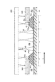
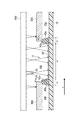
ここで、図3〜図8を参照して、有機エレクトロルミネッセンス膜42の形成について説明する。図3は、蒸着源について説明する図である。図4は、従来例における表示領域の一部を模式的に示す平面図である。図5は、図4のV−V断面図であって、従来例における有機エレクトロルミネッセンス膜の形成について説明する図である。図6は、図4のVI−VI断面図であって、従来例における有機エレクトロルミネッセンス膜の形成について説明する図である。図7は、本実施形態における表示領域の一部を模式的に示す平面図である。図8は、図7のVIII−VIII断面図であって、本実施形態における有機エレクトロルミネッセンス膜の形成について説明する図である。
Here, the formation of the
なお、図5、図6、図8においては、説明の簡略化のため、第1基板10、絶縁層40及び有機エレクトロルミネッセンス膜42以外の層については省略して図示する。また、図5、図6、図8において、絶縁層40の構成の詳細を説明するため、画素領域Pの幅に対する絶縁層40(第1延伸部40a及び第2延伸部40b)の幅の割合を大きくして図示している。図5、図6、図8の矢印は、蒸着源200からの材料の放出を示す。
In FIGS. 5, 6, and 8, layers other than the
有機エレクトロルミネッセンス膜42は、蒸着により発光色毎に塗り分けて形成される。具体的には、図3に示す蒸着源200から有機エレクトロルミネッセンス膜42となる有機材料(以下、単に材料ともいう)が、開口Hを有する蒸着マスク300を介して放出されることにより、蒸着マスク300の開口Hの形状に対応するようにパターン形成される。
The
蒸着源200としては、材料が充填され、複数の放出口200aから材料を放出する所謂ラインソースを用いる。蒸着源200の放出口200aの周辺には、Y方向に沿って放射口200aの一部と重なるように材料の放射角を調整するための遮蔽体200bが設けられている。このため、蒸着源200として、図3中のX方向とY方向とで放出角が異なる。具体的には、蒸着源200として、図3中のY方向を長手とし、X方方向を短手とする形状であり、X方向に最大放出角θ1で材料を放出し、Y方向に最大放出角θ2で材料を放出し、θ1>θ2となる。遮蔽体200abの放出口200aと重なる範囲を調整することにより、最大放出角θ2を調整することができる。一方、最大放出角θ1も同様に調整することができるが、その調整は難しい。これは、調整するためには、複数の遮蔽板もしくは遮蔽板に設けられたスリットが必要であり、それぞれに位置調整が必要なためである。従って、本実施例の通り、一方向のみの放射角を調整する方が製造容易となる。なお、θ1、θ2は0°に近いほど、第1基板10に対して垂直に近い角度で材料が放出されることとなる。図3の領域C1、C2は、材料が放出される領域を模式的に示すものである。
As the
ここで、図4〜図6を参照して、従来例における有機エレクトロルミネッセンス膜42の形成と、その課題について説明する。図4に示すように、各画素領域Pの長辺の長さをa1とし、各画素領域Pの短辺の長さをa2とする。また、絶縁層40の第1延伸部40aの幅をb1とし、絶縁層40の第2延伸部40bの幅をb2とする。従来例においては、図4〜図6に示すように、第1延伸部40aの幅b1と、第2延伸部40bの幅b2とを同じとした。
Here, with reference to FIGS. 4-6, formation of the organic electroluminescent film |
まず、青色の画素領域PBに対応する領域に開口Hを有する蒸着マスク300を、第1延伸部40a上及び第2延伸部40b上に配置する。蒸着マスク300は、平面視において、開口Hの1の端部が第1延伸部40aの幅方向の中央部と重なり、かつ開口Hの他の端部が第2延伸部40bの幅方向の中央部と重なるように配置するとよい。
First, the
そして、絶縁層40が形成される第1基板10を、蒸着源200に対して、スキャン方向Sに相対移動させると共に、蒸着源200から材料を放出する。ここでは、スキャン方向SをX方向とした。
Then, the
図5に示すように、青色の画素領域PB及び第1延伸部40a上には、蒸着源200から最大放出角θ2で放出される材料が蒸着され、青色で発光する有機エレクトロルミネッセンス膜42が形成される。ここで、最大放出角θ2は小さく、第1基板10に対して垂直に近い角度で、青色の画素領域PB及び第1延伸部40a上に放出されるため、有機エレクトロルミネッセンス膜42は略均一の厚さで蒸着されることとなる。
As shown in FIG. 5, a material that is emitted from the
一方、図6に示すように、青色の画素領域PB及び第2延伸部40b上には、蒸着源200から最大放出角θ1で放出される材料が蒸着され、青色で発光する有機エレクトロルミネッセンス膜42が形成される。ここで、最大放出角θ2と比較して最大放出角θ1は大きい。また、蒸着マスク300は、所定の厚みを持っているため、斜めに放出された材料の一部は、蒸着マスク300の開口Hの端部でケラレてしまう。そのため、蒸着マスク300の開口Hの端部付近において、材料が十分に蒸着されず、有機エレクトロルミネッセンス膜42の膜厚が薄い薄膜領域t(蒸着シャドーと呼ばれることもある)が生じることとなる。図6に示すように、薄膜領域tは、第2延伸部40b上であって、有機エレクトロルミネッセンス層42の縁部に生じる。なお、図6中の点線矢印は、蒸着マスク300の開口Hの端部にケラレた材料の本来の進行方向を示す。
On the other hand, as shown in FIG. 6, an
発光領域において有機エレクトロルミネッセンス膜42の薄膜領域tが生じると、その領域への電流が集中し、発光効率の低下の問題が生じるおそれがある。そのため、薄膜領域tが非発光領域である絶縁層40上に形成されるよう、絶縁層40の幅b1、b2が設定されている。なお、ここで、発光領域とは、画素領域Pのうち有機エレクトロルミネッセンス膜42が共通電極44と画素電極36とに挟まれた領域であり、非発光領域とは、画素領域Pのうち絶縁層40の存在により有機エレクトロルミネッセンス膜42と画素電極36が離間した領域である。
When the thin film region t of the
従来例においては、第1延伸部40aの幅b1は、第2延伸部40bの幅b2と同じに設定されている。絶縁層40の幅を広く設定すると、画素領域P間の間隔が大きくなり、高輝度化及び画素の高精細化を実現することの妨げとなってしまう。また、絶縁層40の幅を狭く設定すると、幅b2が狭くなり薄膜領域tが画素領域Pに重なる。これはその領域に電流が集中し、発光効率の低下や短寿命化、色ズレ等の原因となる。
In the conventional example, the width b1 of the first extending
そこで、本実施形態においては、図7、図8に示すように、第1延伸部40aの幅b1を、第2延伸部40bの幅b2よりも狭くした。図8に示すように、青色の画素領域PB及び第1延伸部40a上には、最大放出角θ2で放出される材料が蒸着されることによって、有機エレクトロルミネッセンス膜42が形成される。最大放出角θ2は小さく、第1基板10に対して斜め方向に放出される材料が、蒸着マスク300の開口Hの端部にケラレにくい。そのため、蒸着マスク300の開口Hの端部においても、有機エレクトロルミネッセンス膜42の薄膜領域tが生じにくく、有機エレクトロルミネッセンス膜42は略均一の厚さで形成される。すなわち、第1延伸部40aの幅b1を狭くしても、薄膜領域tに電流が集中することによる発光効率の低下等の問題は生じない。
Therefore, in the present embodiment, as shown in FIGS. 7 and 8, the width b1 of the first extending
本実施形態においては、第1延伸部40aの幅b1を狭くした分、図7に示すX方向における画素領域P間の間隔を狭くでき、画素の高精細化等を実現できる。
In the present embodiment, the interval between the pixel regions P in the X direction shown in FIG. 7 can be narrowed by reducing the width b1 of the first extending
なお、本実施形態において、青色の画素領域PB及び第2延伸部40b上への有機エレクトロルミネッセンス膜42の形成については、従来例で説明した図6と同様であるため、その説明の詳細については省略する。
In the present embodiment, the formation of the
なお、本実施形態においては、第2延伸部40b上に有機エレクトロルミネッセンス膜42の薄膜領域tが形成され、第1延伸部40a上に有機エレクトロルミネッセンス膜42の薄膜領域tが形成されない例について示したが、これに限られるものではない。例えば、第1延伸部40a上に、第2延伸部40b上に形成される薄膜領域tよりも幅の狭い薄膜領域tが形成される構成であってもよい。
In the present embodiment, an example in which the thin film region t of the
なお、本実施形態においては、図7に示すように、Y方向に延びる第1延伸部40aの幅b1を、X方向に延びる第2延伸部40bの幅b2よりも狭くする構成について説明したが、これに限られるものではない。蒸着源200から放出される材料の放出方向及び放出角に依存して、第1延伸部40aと第2延伸部40bのうち、薄膜領域tが生じにくい方のいずれか一方の幅を狭くすればよい。
In the present embodiment, as illustrated in FIG. 7, the configuration has been described in which the width b1 of the first extending
なお、上記においては、青色の画素領域PBに形成される有機エレクトロルミネッセンス膜42についてのみ説明したが、赤色の画素領域PR、緑色の画素領域PGにおいても同様に、各色に対応する有機エレクトロルミネッセンス膜42が蒸着される。
In the above description, only the
さらに、図6、図8、図9、図10を参照して、本実施形態における絶縁層40の詳細について説明する。図9は、本実施形態における絶縁層の傾斜面の傾斜角について説明する図である。図10は、本実施形態におけるハーフトーンマスクを用いた絶縁層の形成について説明する図である。
Furthermore, the details of the insulating
図8等において、絶縁層40の第1延伸部40aは、頂上部41aと、頂上部41aの両端に設けられる傾斜面43aとを有する。絶縁層40の第2延伸部40bは、頂上部41bと、頂上部41bの両端に設けられる傾斜面43bとを有する。図8等においては、絶縁層40の傾斜面が平面である例について示したが、傾斜面は図9のようになだらかな曲面であってもよい。
8 etc., the 1st extending | stretching
以下、図9に示すように、絶縁層40の頂上部41の高さをhとした場合の高さh/2における傾斜面43上の接線と、絶縁層40の底面とが成す角度を、傾斜面43の傾斜角(図9中のα)と定義する。
Hereinafter, as shown in FIG. 9, the angle formed by the tangent on the
本実施形態においては、平面視における第1延伸部40aの頂上部41aの幅を、第2延伸部40bの頂上部41bの幅よりも小さくすることにより、平面視における第1延伸部40aの幅b1を、第2延伸部40bの幅b2よりも小さくした。また、図6、図8に示すように、第1延伸部40aの傾斜面43aの傾斜角を、第2延伸部40bの傾斜面43bの傾斜角より大きくした。
In the present embodiment, the width of the first extending
また、第1延伸部40aの頂上部41aの高さと、第2延伸部40bの頂上部41bの高さは同一とすることが好ましい。蒸着マスク300を、頂上部41a上及び頂上部41b上に載るように配置した場合、それらの高さが異なっていると、蒸着マスク300と絶縁層40との間に隙間が生じることとなり、その隙間から蒸着源200から放出される材料が、隣接する画素領域Pに蒸着されてしまうおそれがあるためである。例えば、青色の画素領域PBに形成する有機エレクトロルミネッセンス膜42が、隣接する赤色の画素領域PRに形成されてしまうと、混色が生じてしまう。
Moreover, it is preferable that the height of the
絶縁層40の傾斜面43は、ハーフトーンマスク400を用いて形成するとよい。図10に示すように、ハーフトーンマスク400は、開口と、遮光部410と、半透過部420を有するとよい。遮光部410は光を遮光し、半透過部42は光を一部透過する。
The
まず、第1基板10上に、絶縁層40を構成する感光性樹脂膜を形成する。そして、感光性樹脂膜上にハーフトーンマスク400を配置して、露光パターニングすることにより絶縁層40の開口及び傾斜面43を形成する。この際、遮光部410が絶縁層40の頂上部41に対応する位置に対応し、半透過部420が傾斜面43に対応する。
First, a photosensitive resin film constituting the insulating
本実施形態においては、第1延伸部40aの傾斜面43aの傾斜角を、第2延伸部40bの傾斜面43bの傾斜角よりも大きくした。例えば、傾斜面43aに対応する位置に半透過部420を設け、傾斜面43bに対応する位置には半透過部420を設けなければよい。また、傾斜面43bにもある程度の傾斜を設ける場合には、いずれの傾斜面に対応する位置にも半透過部420を設けてもよい。例えば、傾斜面43aの傾斜角を70°程度とし、傾斜面43bの傾斜角を30°程度とするとよい。このような構成とするために、傾斜面43aに対応する位置に配置される半透過部420の幅が、傾斜面43bに対応する位置に配置される半透過部420の幅よりも狭いハーフトーンマスク400を用いるとよい。そして、傾斜面43aの傾斜角が傾斜面43bの傾斜角よりも大きくなるように、傾斜面43aと傾斜面43bに対する露光量や露光時間等を異ならせるとよい。
In the present embodiment, the inclination angle of the
以上のように絶縁層40を形成することにより、頂上部41aと頂上部41bの高さを同じとし、第1延伸部40aの幅を第2延伸部40bの幅よりも狭くし、かつ傾斜面43aの傾斜角を傾斜面43bの傾斜角よりも大きい絶縁層40を実現することができる。
By forming the insulating
本発明は、上述した実施形態に限定されるものではなく種々の変形が可能である。例えば、実施形態で説明した構成は、実質的に同一の構成、同一の作用効果を奏する構成又は同一の目的を達成することができる構成で置き換えることができる。 The present invention is not limited to the above-described embodiments, and various modifications can be made. For example, the configuration described in the embodiment can be replaced with substantially the same configuration, a configuration that exhibits the same operational effects, or a configuration that can achieve the same purpose.
10 第1基板、11 第2基板、12 集積回路チップ、16 表示回路層、18 アンダーコート層、20 半導体層、22 ソース電極、24 ドレイン電極、26 ゲート絶縁膜、28 ゲート電極、30 層間絶縁膜、32 パッシベーション膜、34 平坦化層、36 画素電極、38 コンタクトホール、40 絶縁層、40a 第1延伸部、40b 第2延伸部、41 頂上部、42 有機エレクトロルミネッセンス膜、43 傾斜面、44 共通電極、46 発光素子、48 封止層、54 充填層、100 表示装置、200 蒸着源、300 蒸着マスク、400 ハーフトーンマスク、410 遮光部、420 半透過部。 10 first substrate, 11 second substrate, 12 integrated circuit chip, 16 display circuit layer, 18 undercoat layer, 20 semiconductor layer, 22 source electrode, 24 drain electrode, 26 gate insulating film, 28 gate electrode, 30 interlayer insulating film , 32 Passivation film, 34 Planarization layer, 36 Pixel electrode, 38 Contact hole, 40 Insulating layer, 40a First extending portion, 40b Second extending portion, 41 Top, 42 Organic electroluminescence film, 43 Inclined surface, 44 Common Electrode, 46 Light emitting element, 48 Sealing layer, 54 Filling layer, 100 Display device, 200 Deposition source, 300 Deposition mask, 400 Halftone mask, 410 Light-shielding part, 420 Semi-transmissive part
Claims (7)
前記画素領域、前記第1延伸部上、及び前記第2延伸部上に形成される有機エレクトロルミネッセンス膜と、
を有し、
平面視における、前記第1延伸部の幅は、前記第2延伸部の幅よりも小さい、
表示装置。 Insulation partitioning the pixel region by a first extending portion extending in a direction along the first side of the pixel region and a second extending portion extending in a direction along the second side intersecting the first side of the pixel region. Layers,
An organic electroluminescence film formed on the pixel region, the first extending portion, and the second extending portion;
Have
In plan view, the width of the first extending portion is smaller than the width of the second extending portion.
Display device.
前記第2延伸部は、第2頂上部と、前記第2頂上部の幅方向の両端に形成される第2傾斜面とを有し、
前記第1傾斜面は、前記第2傾斜面よりも傾斜角が大きい、
請求項1又は2に記載の表示装置。 The first extending portion has a first apex portion and first inclined surfaces formed at both ends in the width direction of the first apex portion,
The second extending portion has a second top and second inclined surfaces formed at both ends in the width direction of the second top,
The first inclined surface has a larger inclination angle than the second inclined surface;
The display device according to claim 1.
請求項3に記載の表示装置。 The first top is smaller in width in plan view than the second top.
The display device according to claim 3.
請求項3に記載の表示装置。 The first top and the second top are the same height.
The display device according to claim 3.
前記第2辺は前記長辺であり、前記第1辺は前記短辺である請求項1〜5のいずれかに記載の表示装置。 The pixel region has a long side and a short side in plan view,
The display device according to claim 1, wherein the second side is the long side, and the first side is the short side.
前記有機エレクトロルミネッセンス膜は、発光色毎に複数の前記画素領域のそれぞれに形成される請求項1〜6のいずれかに記載の表示装置。 A plurality of the pixel regions are arranged in a matrix,
The display device according to claim 1, wherein the organic electroluminescence film is formed in each of the plurality of pixel regions for each emission color.
Priority Applications (2)
| Application Number | Priority Date | Filing Date | Title |
|---|---|---|---|
| JP2017166438A JP2019046599A (en) | 2017-08-31 | 2017-08-31 | Display device |
| US16/112,876 US11211436B2 (en) | 2017-08-31 | 2018-08-27 | Display device |
Applications Claiming Priority (1)
| Application Number | Priority Date | Filing Date | Title |
|---|---|---|---|
| JP2017166438A JP2019046599A (en) | 2017-08-31 | 2017-08-31 | Display device |
Publications (1)
| Publication Number | Publication Date |
|---|---|
| JP2019046599A true JP2019046599A (en) | 2019-03-22 |
Family
ID=65437755
Family Applications (1)
| Application Number | Title | Priority Date | Filing Date |
|---|---|---|---|
| JP2017166438A Pending JP2019046599A (en) | 2017-08-31 | 2017-08-31 | Display device |
Country Status (2)
| Country | Link |
|---|---|
| US (1) | US11211436B2 (en) |
| JP (1) | JP2019046599A (en) |
Families Citing this family (1)
| Publication number | Priority date | Publication date | Assignee | Title |
|---|---|---|---|---|
| CN111155055A (en) * | 2020-01-06 | 2020-05-15 | 武汉华星光电半导体显示技术有限公司 | OLED panel, evaporation method thereof and mask set thereof |
Family Cites Families (8)
| Publication number | Priority date | Publication date | Assignee | Title |
|---|---|---|---|---|
| JP4053209B2 (en) * | 2000-05-01 | 2008-02-27 | 三星エスディアイ株式会社 | Manufacturing method of organic EL display |
| US20020197393A1 (en) * | 2001-06-08 | 2002-12-26 | Hideaki Kuwabara | Process of manufacturing luminescent device |
| KR100508002B1 (en) * | 2002-09-03 | 2005-08-17 | 엘지.필립스 엘시디 주식회사 | fabrication method of an organic electro-luminescence device using nozzle coating |
| JP3915810B2 (en) * | 2004-02-26 | 2007-05-16 | セイコーエプソン株式会社 | ORGANIC ELECTROLUMINESCENCE DEVICE, ITS MANUFACTURING METHOD, AND ELECTRONIC DEVICE |
| JP4812627B2 (en) * | 2004-10-28 | 2011-11-09 | シャープ株式会社 | ORGANIC ELECTROLUMINESCENCE PANEL AND MANUFACTURING METHOD THEREOF, COLOR FILTER SUBSTRATE AND ITS MANUFACTURING METHOD |
| TWI486097B (en) | 2008-12-01 | 2015-05-21 | 半導體能源研究所股份有限公司 | Light-emitting element, light-emitting device, lighting device, and electronic device |
| JP2011216250A (en) * | 2010-03-31 | 2011-10-27 | Sumitomo Chemical Co Ltd | Manufacturing method of substrate for organic el element |
| JP2016091942A (en) * | 2014-11-10 | 2016-05-23 | 株式会社Joled | Display device and manufacturing method thereof |
-
2017
- 2017-08-31 JP JP2017166438A patent/JP2019046599A/en active Pending
-
2018
- 2018-08-27 US US16/112,876 patent/US11211436B2/en active Active
Also Published As
| Publication number | Publication date |
|---|---|
| US20190067393A1 (en) | 2019-02-28 |
| US11211436B2 (en) | 2021-12-28 |
Similar Documents
| Publication | Publication Date | Title |
|---|---|---|
| US9887246B2 (en) | Organic light emitting display panel and device with a black bank in a planarization layer | |
| JP6995489B2 (en) | Display device | |
| CN107863366B (en) | Organic Light Emitting Diode Display Device | |
| US9825109B2 (en) | Display device | |
| CN110752242B (en) | Display panel and display device | |
| KR20180045942A (en) | Flat Panel Display Connecting Front Side to Rear Side of Substrate Using Through Hole | |
| US11018200B2 (en) | Display device having a white emitting area | |
| KR102724354B1 (en) | Organic light emitting display device | |
| KR20180073065A (en) | Display device having a color filter | |
| KR20230153321A (en) | Organic light-emitting display apparatus | |
| KR20210080925A (en) | Electroluminescent Device | |
| KR102138859B1 (en) | Organic light emitting diode display and manufacturing method thereof | |
| JP2018006232A (en) | Display device and manufacturing method thereof | |
| US20240237457A1 (en) | Pixel arrangement structure, display panel and method for manufacturing the same | |
| JP6870950B2 (en) | Display device | |
| JP2019110271A (en) | Display device | |
| WO2019186629A1 (en) | Vapor deposition mask, vapor deposition mask set, vapor deposition mask manufacturing method, vapor deposition mask set manufacturing method, and display device manufacturing method | |
| CN112640580B (en) | Display device and method for manufacturing the same | |
| JP2019046599A (en) | Display device | |
| CN111819910B (en) | display device | |
| JP2018116769A (en) | Display device | |
| US12310184B2 (en) | Display device and manufacturing method therefor | |
| WO2023004631A1 (en) | Array substrate, display apparatus, and method of fabricating array substrate | |
| JP2023078010A (en) | Display device | |
| KR20200091373A (en) | Organic light emitting diode display and manufacturing method thereof |