JP2019061202A - 表示装置 - Google Patents
表示装置 Download PDFInfo
- Publication number
- JP2019061202A JP2019061202A JP2017187686A JP2017187686A JP2019061202A JP 2019061202 A JP2019061202 A JP 2019061202A JP 2017187686 A JP2017187686 A JP 2017187686A JP 2017187686 A JP2017187686 A JP 2017187686A JP 2019061202 A JP2019061202 A JP 2019061202A
- Authority
- JP
- Japan
- Prior art keywords
- display device
- scanning
- line group
- group
- scanning line
- Prior art date
- Legal status (The legal status is an assumption and is not a legal conclusion. Google has not performed a legal analysis and makes no representation as to the accuracy of the status listed.)
- Granted
Links
Images






Classifications
-
- G—PHYSICS
- G02—OPTICS
- G02F—OPTICAL DEVICES OR ARRANGEMENTS FOR THE CONTROL OF LIGHT BY MODIFICATION OF THE OPTICAL PROPERTIES OF THE MEDIA OF THE ELEMENTS INVOLVED THEREIN; NON-LINEAR OPTICS; FREQUENCY-CHANGING OF LIGHT; OPTICAL LOGIC ELEMENTS; OPTICAL ANALOGUE/DIGITAL CONVERTERS
- G02F1/00—Devices or arrangements for the control of the intensity, colour, phase, polarisation or direction of light arriving from an independent light source, e.g. switching, gating or modulating; Non-linear optics
- G02F1/01—Devices or arrangements for the control of the intensity, colour, phase, polarisation or direction of light arriving from an independent light source, e.g. switching, gating or modulating; Non-linear optics for the control of the intensity, phase, polarisation or colour
- G02F1/13—Devices or arrangements for the control of the intensity, colour, phase, polarisation or direction of light arriving from an independent light source, e.g. switching, gating or modulating; Non-linear optics for the control of the intensity, phase, polarisation or colour based on liquid crystals, e.g. single liquid crystal display cells
- G02F1/133—Constructional arrangements; Operation of liquid crystal cells; Circuit arrangements
- G02F1/136—Liquid crystal cells structurally associated with a semi-conducting layer or substrate, e.g. cells forming part of an integrated circuit
- G02F1/1362—Active matrix addressed cells
- G02F1/136286—Wiring, e.g. gate line, drain line
-
- G—PHYSICS
- G09—EDUCATION; CRYPTOGRAPHY; DISPLAY; ADVERTISING; SEALS
- G09G—ARRANGEMENTS OR CIRCUITS FOR CONTROL OF INDICATING DEVICES USING STATIC MEANS TO PRESENT VARIABLE INFORMATION
- G09G3/00—Control arrangements or circuits, of interest only in connection with visual indicators other than cathode-ray tubes
- G09G3/20—Control arrangements or circuits, of interest only in connection with visual indicators other than cathode-ray tubes for presentation of an assembly of a number of characters, e.g. a page, by composing the assembly by combination of individual elements arranged in a matrix no fixed position being assigned to or needed to be assigned to the individual characters or partial characters
- G09G3/34—Control arrangements or circuits, of interest only in connection with visual indicators other than cathode-ray tubes for presentation of an assembly of a number of characters, e.g. a page, by composing the assembly by combination of individual elements arranged in a matrix no fixed position being assigned to or needed to be assigned to the individual characters or partial characters by control of light from an independent source
- G09G3/36—Control arrangements or circuits, of interest only in connection with visual indicators other than cathode-ray tubes for presentation of an assembly of a number of characters, e.g. a page, by composing the assembly by combination of individual elements arranged in a matrix no fixed position being assigned to or needed to be assigned to the individual characters or partial characters by control of light from an independent source using liquid crystals
- G09G3/3611—Control of matrices with row and column drivers
- G09G3/3674—Details of drivers for scan electrodes
-
- G—PHYSICS
- G09—EDUCATION; CRYPTOGRAPHY; DISPLAY; ADVERTISING; SEALS
- G09G—ARRANGEMENTS OR CIRCUITS FOR CONTROL OF INDICATING DEVICES USING STATIC MEANS TO PRESENT VARIABLE INFORMATION
- G09G3/00—Control arrangements or circuits, of interest only in connection with visual indicators other than cathode-ray tubes
- G09G3/20—Control arrangements or circuits, of interest only in connection with visual indicators other than cathode-ray tubes for presentation of an assembly of a number of characters, e.g. a page, by composing the assembly by combination of individual elements arranged in a matrix no fixed position being assigned to or needed to be assigned to the individual characters or partial characters
- G09G3/34—Control arrangements or circuits, of interest only in connection with visual indicators other than cathode-ray tubes for presentation of an assembly of a number of characters, e.g. a page, by composing the assembly by combination of individual elements arranged in a matrix no fixed position being assigned to or needed to be assigned to the individual characters or partial characters by control of light from an independent source
- G09G3/36—Control arrangements or circuits, of interest only in connection with visual indicators other than cathode-ray tubes for presentation of an assembly of a number of characters, e.g. a page, by composing the assembly by combination of individual elements arranged in a matrix no fixed position being assigned to or needed to be assigned to the individual characters or partial characters by control of light from an independent source using liquid crystals
- G09G3/3611—Control of matrices with row and column drivers
- G09G3/3674—Details of drivers for scan electrodes
- G09G3/3677—Details of drivers for scan electrodes suitable for active matrices only
-
- H—ELECTRICITY
- H10—SEMICONDUCTOR DEVICES; ELECTRIC SOLID-STATE DEVICES NOT OTHERWISE PROVIDED FOR
- H10D—INORGANIC ELECTRIC SEMICONDUCTOR DEVICES
- H10D86/00—Integrated devices formed in or on insulating or conducting substrates, e.g. formed in silicon-on-insulator [SOI] substrates or on stainless steel or glass substrates
- H10D86/40—Integrated devices formed in or on insulating or conducting substrates, e.g. formed in silicon-on-insulator [SOI] substrates or on stainless steel or glass substrates characterised by multiple TFTs
- H10D86/441—Interconnections, e.g. scanning lines
-
- H—ELECTRICITY
- H10—SEMICONDUCTOR DEVICES; ELECTRIC SOLID-STATE DEVICES NOT OTHERWISE PROVIDED FOR
- H10D—INORGANIC ELECTRIC SEMICONDUCTOR DEVICES
- H10D86/00—Integrated devices formed in or on insulating or conducting substrates, e.g. formed in silicon-on-insulator [SOI] substrates or on stainless steel or glass substrates
- H10D86/40—Integrated devices formed in or on insulating or conducting substrates, e.g. formed in silicon-on-insulator [SOI] substrates or on stainless steel or glass substrates characterised by multiple TFTs
- H10D86/60—Integrated devices formed in or on insulating or conducting substrates, e.g. formed in silicon-on-insulator [SOI] substrates or on stainless steel or glass substrates characterised by multiple TFTs wherein the TFTs are in active matrices
-
- G—PHYSICS
- G02—OPTICS
- G02F—OPTICAL DEVICES OR ARRANGEMENTS FOR THE CONTROL OF LIGHT BY MODIFICATION OF THE OPTICAL PROPERTIES OF THE MEDIA OF THE ELEMENTS INVOLVED THEREIN; NON-LINEAR OPTICS; FREQUENCY-CHANGING OF LIGHT; OPTICAL LOGIC ELEMENTS; OPTICAL ANALOGUE/DIGITAL CONVERTERS
- G02F2201/00—Constructional arrangements not provided for in groups G02F1/00 - G02F7/00
- G02F2201/56—Substrates having a particular shape, e.g. non-rectangular
-
- G—PHYSICS
- G09—EDUCATION; CRYPTOGRAPHY; DISPLAY; ADVERTISING; SEALS
- G09G—ARRANGEMENTS OR CIRCUITS FOR CONTROL OF INDICATING DEVICES USING STATIC MEANS TO PRESENT VARIABLE INFORMATION
- G09G2300/00—Aspects of the constitution of display devices
- G09G2300/04—Structural and physical details of display devices
- G09G2300/0421—Structural details of the set of electrodes
- G09G2300/0426—Layout of electrodes and connections
-
- G—PHYSICS
- G09—EDUCATION; CRYPTOGRAPHY; DISPLAY; ADVERTISING; SEALS
- G09G—ARRANGEMENTS OR CIRCUITS FOR CONTROL OF INDICATING DEVICES USING STATIC MEANS TO PRESENT VARIABLE INFORMATION
- G09G2310/00—Command of the display device
- G09G2310/02—Addressing, scanning or driving the display screen or processing steps related thereto
- G09G2310/0232—Special driving of display border areas
-
- G—PHYSICS
- G09—EDUCATION; CRYPTOGRAPHY; DISPLAY; ADVERTISING; SEALS
- G09G—ARRANGEMENTS OR CIRCUITS FOR CONTROL OF INDICATING DEVICES USING STATIC MEANS TO PRESENT VARIABLE INFORMATION
- G09G2320/00—Control of display operating conditions
- G09G2320/02—Improving the quality of display appearance
- G09G2320/0233—Improving the luminance or brightness uniformity across the screen
-
- H—ELECTRICITY
- H10—SEMICONDUCTOR DEVICES; ELECTRIC SOLID-STATE DEVICES NOT OTHERWISE PROVIDED FOR
- H10K—ORGANIC ELECTRIC SOLID-STATE DEVICES
- H10K59/00—Integrated devices, or assemblies of multiple devices, comprising at least one organic light-emitting element covered by group H10K50/00
- H10K59/10—OLED displays
- H10K59/12—Active-matrix OLED [AMOLED] displays
- H10K59/131—Interconnections, e.g. wiring lines or terminals
Landscapes
- Physics & Mathematics (AREA)
- Engineering & Computer Science (AREA)
- General Physics & Mathematics (AREA)
- Crystallography & Structural Chemistry (AREA)
- Chemical & Material Sciences (AREA)
- Nonlinear Science (AREA)
- Theoretical Computer Science (AREA)
- Computer Hardware Design (AREA)
- Microelectronics & Electronic Packaging (AREA)
- Mathematical Physics (AREA)
- Optics & Photonics (AREA)
- Devices For Indicating Variable Information By Combining Individual Elements (AREA)
- Liquid Crystal (AREA)
Abstract
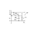
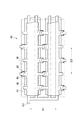
【解決手段】表示装置は、基板10と、基板10上に設けられた複数の信号線Sと、基板10上に設けられ、信号線Sと交差する複数の走査線Gと、走査線Gと信号線Sの交差位置に形成された複数の薄膜トランジスタTFTと、を有する。走査線Gは、第1の走査線群G1と、第2の走査線群G2を有し、第2の走査線群GSの走査線Gの一端は、負荷素子40が接続される。
【選択図】図5
Description
Claims (16)
- 基板と、
前記基板上に設けられた複数の信号線と、
前記基板上に設けられ、前記信号線と交差する複数の走査線と、
前記走査線と信号線の交差位置に形成された複数の薄膜トランジスタと、
を有し、
前記走査線は、第1の走査線群と、第2の走査線群を有し、
前記第2の走査線群の前記走査線の一端は、負荷素子が接続されることを特徴とする表示装置。 - 請求項1に記載された表示装置において、
前記第1の走査線群と前記第2の走査線群は、隣接して配置され、
前記基板は、前記第2走査線群の走査線の延在方向に重なる位置に切欠き部を有することを特徴とする表示装置。 - 請求項2に記載された表示装置において、
前記負荷素子は、複数の電界効果素子からなることを特徴とする表示装置。 - 請求項3に記載された表示装置において、
前記複数の電界効果素子は、第1の走査線群に近い走査線程、接続される電界効果素子の数が増えることを特徴とする表示装置。 - 請求項2に記載された表示装置において、
前記基板は、第3の走査線群を有し、
前記第3の走査線群の走査線延在方向は、前記切欠き部と重なり、
前記第2の走査線群は、前記第1の走査線群と前記第3の走査線群の間に配置され、
前記第3の走査線群の前記走査線の一端は、負荷素子が接続されることを特徴とする表示装置。 - 請求項5に記載された表示装置において、
前記基板は、表示領域と非表示領域を有し、
前記第2走査線群と前記第3走査線群の前記負荷素子は、前記切欠き部と前記表示領域間の前記非表示領域に形成されていることを特徴とする表示装置。 - 請求項6に記載された表示装置において、
前記第2の走査線群の前記負荷素子は、複数の電界効果素子からなることを特徴とする表示装置。 - 請求項7に記載された表示装置において、
前記第2の走査線群の各走査線は、前記非表示領域において、信号線と平行に延設された屈曲部を有することを特徴とする表示装置。 - 請求項7に記載された表示装置において、
前記第2の走査線群の前記負荷素子は、半導体層と導電層を含む複数の薄膜トランジスタからなることを特徴とする表示装置。 - 請求項9に記載された表示装置において、
前記第3の走査線群の前記負荷素子は、前記走査線に絶縁膜を介して重畳された半導体層又は導電層であり、
前記第3の走査線群の複数の前記負荷素子は、同じ形状であることを特徴とする表示装置。 - 請求項10に記載された表示装置において、
前記第2の走査線群の前記負荷素子が有する前記半導体層および前記導電層は、
前記第3の走査線群の前記負荷素子が有する前記半導体層および前記導電層と同じ層で形成されることを特徴とする表示装置。 - 請求項5に記載された表示装置において、
前記表示領域における前記第2及び第3の走査線群の走査線の長さは、前記表示領域における前記第1の走査線群の走査線の長さの半分以下であることを特徴とする表示装置。 - 請求項5に記載された表示装置において、
ブラックマトリクス層をさらに有し、
前記複数の負荷素子は、前記ブラックマトリクス層に重なることを特徴とする表示装置。 - 請求項5に記載された表示装置において、
前記複数の走査線が接続される走査回路をさらに有し、
前記第2及び第3の走査線群の一端は、前記走査回路に接続されることを特徴とする表示装置。 - 請求項14に記載された表示装置において、
前記基板は、4辺を有する略矩形状を有し、前記切欠き部は前記基板の1辺に形成され、
前記走査回路は、前記切欠き部が形成されていない辺の向かい合う2辺に形成されることを特徴とする表示装置。 - 請求項15に記載された表示装置において、
前記第1の走査線群は、2辺に設けられた前記走査回路の両方に接続され、
前記第2及び第3の走査線群は、片方の前記走査回路に接続されることを特徴とする表示装置。
Priority Applications (7)
| Application Number | Priority Date | Filing Date | Title |
|---|---|---|---|
| JP2017187686A JP6938312B2 (ja) | 2017-09-28 | 2017-09-28 | 表示装置 |
| US16/132,908 US10651207B2 (en) | 2017-09-28 | 2018-09-17 | Display device having a scanning circuit disposed along an edge of a substrate and scan lines connected to the scanning circuit |
| US16/839,121 US11171162B2 (en) | 2017-09-28 | 2020-04-03 | Display device having scan lines of different lengths |
| JP2021140135A JP7142756B2 (ja) | 2017-09-28 | 2021-08-30 | 表示装置 |
| US17/501,014 US12027531B2 (en) | 2017-09-28 | 2021-10-14 | Display device |
| US18/673,892 US12376381B2 (en) | 2017-09-28 | 2024-05-24 | Display device |
| US19/251,938 US20250324761A1 (en) | 2017-09-28 | 2025-06-27 | Display device |
Applications Claiming Priority (1)
| Application Number | Priority Date | Filing Date | Title |
|---|---|---|---|
| JP2017187686A JP6938312B2 (ja) | 2017-09-28 | 2017-09-28 | 表示装置 |
Related Child Applications (1)
| Application Number | Title | Priority Date | Filing Date |
|---|---|---|---|
| JP2021140135A Division JP7142756B2 (ja) | 2017-09-28 | 2021-08-30 | 表示装置 |
Publications (2)
| Publication Number | Publication Date |
|---|---|
| JP2019061202A true JP2019061202A (ja) | 2019-04-18 |
| JP6938312B2 JP6938312B2 (ja) | 2021-09-22 |
Family
ID=65807816
Family Applications (2)
| Application Number | Title | Priority Date | Filing Date |
|---|---|---|---|
| JP2017187686A Active JP6938312B2 (ja) | 2017-09-28 | 2017-09-28 | 表示装置 |
| JP2021140135A Active JP7142756B2 (ja) | 2017-09-28 | 2021-08-30 | 表示装置 |
Family Applications After (1)
| Application Number | Title | Priority Date | Filing Date |
|---|---|---|---|
| JP2021140135A Active JP7142756B2 (ja) | 2017-09-28 | 2021-08-30 | 表示装置 |
Country Status (2)
| Country | Link |
|---|---|
| US (5) | US10651207B2 (ja) |
| JP (2) | JP6938312B2 (ja) |
Cited By (3)
| Publication number | Priority date | Publication date | Assignee | Title |
|---|---|---|---|---|
| JP2019070744A (ja) * | 2017-10-10 | 2019-05-09 | 三菱電機株式会社 | 液晶表示装置 |
| US12223922B2 (en) | 2022-07-05 | 2025-02-11 | Japan Display Inc. | Display device |
| WO2026028334A1 (ja) * | 2024-07-31 | 2026-02-05 | シャープディスプレイテクノロジー株式会社 | 表示パネル |
Families Citing this family (10)
| Publication number | Priority date | Publication date | Assignee | Title |
|---|---|---|---|---|
| CN206074968U (zh) * | 2016-10-14 | 2017-04-05 | 京东方科技集团股份有限公司 | 阵列基板及显示装置 |
| KR102362704B1 (ko) | 2017-09-07 | 2022-02-14 | 삼성디스플레이 주식회사 | 유기 발광 표시 장치 |
| JP6938312B2 (ja) | 2017-09-28 | 2021-09-22 | 株式会社ジャパンディスプレイ | 表示装置 |
| JP2019078977A (ja) | 2017-10-27 | 2019-05-23 | 株式会社ジャパンディスプレイ | 表示装置 |
| KR102525343B1 (ko) * | 2018-04-09 | 2023-04-26 | 삼성디스플레이 주식회사 | 유기 발광 표시 장치 |
| KR102644863B1 (ko) * | 2019-03-19 | 2024-03-11 | 삼성디스플레이 주식회사 | 표시 장치 |
| US11099442B2 (en) * | 2019-07-01 | 2021-08-24 | Sharp Kabushiki Kaisha | Display device |
| US12082460B2 (en) * | 2020-02-27 | 2024-09-03 | Chengdu Boe Optoelectronics Technology Co., Ltd. | Display substrate and manufacturing method thereof, and display apparatus |
| CN116206559B (zh) * | 2021-11-30 | 2025-08-05 | 合肥京东方光电科技有限公司 | 显示基板和显示装置 |
| WO2023127161A1 (ja) * | 2021-12-29 | 2023-07-06 | シャープディスプレイテクノロジー株式会社 | 表示装置 |
Citations (7)
| Publication number | Priority date | Publication date | Assignee | Title |
|---|---|---|---|---|
| WO2007105700A1 (ja) * | 2006-03-15 | 2007-09-20 | Sharp Kabushiki Kaisha | アクティブマトリクス基板およびそれを用いた表示装置 |
| WO2007132574A1 (ja) * | 2006-05-12 | 2007-11-22 | Sharp Kabushiki Kaisha | 表示パネル及び表示装置 |
| WO2009057342A1 (ja) * | 2007-10-31 | 2009-05-07 | Sharp Kabushiki Kaisha | 表示パネル及び表示装置 |
| JP2010164765A (ja) * | 2009-01-15 | 2010-07-29 | Toshiba Mobile Display Co Ltd | 液晶表示装置 |
| WO2014142183A1 (ja) * | 2013-03-15 | 2014-09-18 | シャープ株式会社 | アクティブマトリクス基板、アクティブマトリクス基板の製造方法、及び表示パネル |
| US20160035284A1 (en) * | 2014-07-31 | 2016-02-04 | Lg Display Co., Ltd. | Bridge lines for powering a small form factor oled display device |
| JP2018534613A (ja) * | 2016-03-28 | 2018-11-22 | アップル インコーポレイテッドApple Inc. | 発光ダイオードディスプレイ |
Family Cites Families (8)
| Publication number | Priority date | Publication date | Assignee | Title |
|---|---|---|---|---|
| KR101346246B1 (ko) * | 2006-08-24 | 2013-12-31 | 가부시키가이샤 한도오따이 에네루기 켄큐쇼 | 표시장치 제작방법 |
| JP4659885B2 (ja) * | 2006-11-21 | 2011-03-30 | シャープ株式会社 | アクティブマトリクス基板、表示パネル、及び表示装置 |
| JP5532481B2 (ja) * | 2009-05-13 | 2014-06-25 | Nltテクノロジー株式会社 | カラー画像表示方式、カラーフィルタ基板、カラー画素アレイ基板、画像表示装置及び電子機器 |
| KR102276995B1 (ko) * | 2015-02-12 | 2021-07-21 | 삼성디스플레이 주식회사 | 비사각형 디스플레이 |
| KR102546135B1 (ko) * | 2015-09-28 | 2023-06-20 | 애플 인크. | 연장된 활성 영역을 갖는 전자 디바이스 디스플레이 |
| KR102483956B1 (ko) * | 2016-03-31 | 2023-01-03 | 삼성디스플레이 주식회사 | 디스플레이 장치 |
| CN106448587B (zh) * | 2016-10-08 | 2019-09-20 | 京东方科技集团股份有限公司 | 显示面板及其制造方法、显示装置 |
| JP6938312B2 (ja) * | 2017-09-28 | 2021-09-22 | 株式会社ジャパンディスプレイ | 表示装置 |
-
2017
- 2017-09-28 JP JP2017187686A patent/JP6938312B2/ja active Active
-
2018
- 2018-09-17 US US16/132,908 patent/US10651207B2/en active Active
-
2020
- 2020-04-03 US US16/839,121 patent/US11171162B2/en active Active
-
2021
- 2021-08-30 JP JP2021140135A patent/JP7142756B2/ja active Active
- 2021-10-14 US US17/501,014 patent/US12027531B2/en active Active
-
2024
- 2024-05-24 US US18/673,892 patent/US12376381B2/en active Active
-
2025
- 2025-06-27 US US19/251,938 patent/US20250324761A1/en active Pending
Patent Citations (7)
| Publication number | Priority date | Publication date | Assignee | Title |
|---|---|---|---|---|
| WO2007105700A1 (ja) * | 2006-03-15 | 2007-09-20 | Sharp Kabushiki Kaisha | アクティブマトリクス基板およびそれを用いた表示装置 |
| WO2007132574A1 (ja) * | 2006-05-12 | 2007-11-22 | Sharp Kabushiki Kaisha | 表示パネル及び表示装置 |
| WO2009057342A1 (ja) * | 2007-10-31 | 2009-05-07 | Sharp Kabushiki Kaisha | 表示パネル及び表示装置 |
| JP2010164765A (ja) * | 2009-01-15 | 2010-07-29 | Toshiba Mobile Display Co Ltd | 液晶表示装置 |
| WO2014142183A1 (ja) * | 2013-03-15 | 2014-09-18 | シャープ株式会社 | アクティブマトリクス基板、アクティブマトリクス基板の製造方法、及び表示パネル |
| US20160035284A1 (en) * | 2014-07-31 | 2016-02-04 | Lg Display Co., Ltd. | Bridge lines for powering a small form factor oled display device |
| JP2018534613A (ja) * | 2016-03-28 | 2018-11-22 | アップル インコーポレイテッドApple Inc. | 発光ダイオードディスプレイ |
Cited By (4)
| Publication number | Priority date | Publication date | Assignee | Title |
|---|---|---|---|---|
| JP2019070744A (ja) * | 2017-10-10 | 2019-05-09 | 三菱電機株式会社 | 液晶表示装置 |
| USRE50155E1 (en) | 2017-10-10 | 2024-10-01 | Trivale Technologies | Liquid crystal display device |
| US12223922B2 (en) | 2022-07-05 | 2025-02-11 | Japan Display Inc. | Display device |
| WO2026028334A1 (ja) * | 2024-07-31 | 2026-02-05 | シャープディスプレイテクノロジー株式会社 | 表示パネル |
Also Published As
| Publication number | Publication date |
|---|---|
| JP6938312B2 (ja) | 2021-09-22 |
| US20250324761A1 (en) | 2025-10-16 |
| US12376381B2 (en) | 2025-07-29 |
| US10651207B2 (en) | 2020-05-12 |
| US11171162B2 (en) | 2021-11-09 |
| JP2021193450A (ja) | 2021-12-23 |
| JP7142756B2 (ja) | 2022-09-27 |
| US20190096914A1 (en) | 2019-03-28 |
| US20220037367A1 (en) | 2022-02-03 |
| US20200235129A1 (en) | 2020-07-23 |
| US20240313004A1 (en) | 2024-09-19 |
| US12027531B2 (en) | 2024-07-02 |
Similar Documents
| Publication | Publication Date | Title |
|---|---|---|
| JP7142756B2 (ja) | 表示装置 | |
| US11675241B2 (en) | Display device | |
| CN102648436B (zh) | 液晶显示装置 | |
| US10175818B2 (en) | Display device | |
| CN205405027U (zh) | 显示装置 | |
| JP6962759B2 (ja) | 表示装置 | |
| CN110164388A (zh) | 显示面板 | |
| US10622384B2 (en) | Liquid crystal display panel and liquid crystal display | |
| US11237443B2 (en) | Display device | |
| WO2009104346A1 (ja) | アクティブマトリクス基板及び液晶表示装置 | |
| KR20100100228A (ko) | 표시 장치 | |
| US20230037791A1 (en) | Display device | |
| JP5154786B2 (ja) | 液晶表示装置 | |
| JP6727952B2 (ja) | 表示装置 | |
| EP2175439A2 (en) | Liquid crystal display (LCD) panel and pixel driving device therefor | |
| US11927869B2 (en) | Semiconductor substrate and a display device incorporating the semiconductor substrate | |
| US10409125B2 (en) | Display device |
Legal Events
| Date | Code | Title | Description |
|---|---|---|---|
| A621 | Written request for application examination |
Free format text: JAPANESE INTERMEDIATE CODE: A621 Effective date: 20200908 |
|
| A977 | Report on retrieval |
Free format text: JAPANESE INTERMEDIATE CODE: A971007 Effective date: 20210519 |
|
| A131 | Notification of reasons for refusal |
Free format text: JAPANESE INTERMEDIATE CODE: A131 Effective date: 20210525 |
|
| A521 | Request for written amendment filed |
Free format text: JAPANESE INTERMEDIATE CODE: A523 Effective date: 20210716 |
|
| TRDD | Decision of grant or rejection written | ||
| A01 | Written decision to grant a patent or to grant a registration (utility model) |
Free format text: JAPANESE INTERMEDIATE CODE: A01 Effective date: 20210803 |
|
| A61 | First payment of annual fees (during grant procedure) |
Free format text: JAPANESE INTERMEDIATE CODE: A61 Effective date: 20210901 |
|
| R150 | Certificate of patent or registration of utility model |
Ref document number: 6938312 Country of ref document: JP Free format text: JAPANESE INTERMEDIATE CODE: R150 |
|
| R250 | Receipt of annual fees |
Free format text: JAPANESE INTERMEDIATE CODE: R250 |
|
| S111 | Request for change of ownership or part of ownership |
Free format text: JAPANESE INTERMEDIATE CODE: R313113 |
|
| R350 | Written notification of registration of transfer |
Free format text: JAPANESE INTERMEDIATE CODE: R350 |
|
| R250 | Receipt of annual fees |
Free format text: JAPANESE INTERMEDIATE CODE: R250 |