JP2019078563A - Directional coupler - Google Patents
Directional coupler Download PDFInfo
- Publication number
- JP2019078563A JP2019078563A JP2017203732A JP2017203732A JP2019078563A JP 2019078563 A JP2019078563 A JP 2019078563A JP 2017203732 A JP2017203732 A JP 2017203732A JP 2017203732 A JP2017203732 A JP 2017203732A JP 2019078563 A JP2019078563 A JP 2019078563A
- Authority
- JP
- Japan
- Prior art keywords
- detector
- detection unit
- wiring board
- printed wiring
- directional coupler
- Prior art date
- Legal status (The legal status is an assumption and is not a legal conclusion. Google has not performed a legal analysis and makes no representation as to the accuracy of the status listed.)
- Granted
Links
Images






Landscapes
- Measuring Instrument Details And Bridges, And Automatic Balancing Devices (AREA)
- Plasma Technology (AREA)
Abstract
【課題】進行波と反射波の測定を安定して行うことができる方向性結合器を提供する。【解決手段】湾曲した金属板から成る検出器23aと、プリント配線板25に形成した金属膜の内部配線43とによって巻線を形成し、導電線15に流れる電流が形成する磁束によって巻線に起電力を発生させ、終端回路24によって、進行波と反射波とを区別して検出する。検出器23aと内部配線43とで構成された巻線の芯は空気なので、巻線の電気的特性は温度変化の影響を受けない。【選択図】図2PROBLEM TO BE SOLVED: To provide a directional coupler capable of stably measuring a traveling wave and a reflected wave. SOLUTION: A winding is formed by a detector 23a made of a curved metal plate and an internal wiring 43 of a metal film formed on a printed wiring board 25, and the winding is formed by a magnetic flux formed by a current flowing through a conductive wire 15. An electromotive force is generated, and a traveling wave and a reflected wave are detected separately by the termination circuit 24. Since the core of the winding composed of the detector 23a and the internal wiring 43 is air, the electrical characteristics of the winding are not affected by the temperature change. [Selection diagram] Fig. 2
Description
本発明は進行波と反射波とを検出する方向性結合器に関する。 The present invention relates to a directional coupler that detects a traveling wave and a reflected wave.
近年の半導体製造装置の処理技術高度化にともない、プラズマプロセスにおける高周波電力の高精度な測定、精緻な制御が必要とされている。 With the advancement of processing technology of semiconductor manufacturing equipment in recent years, high-precision measurement and fine control of high-frequency power in plasma processing are required.
伝送線路上を通過する高周波電力を測定する方法としては、特許第3,299,273号公報に代表されるように、伝送線路に発生している電磁界を利用して、2つの高周波信号を検出し、処理する方法が主流である。 As a method of measuring high frequency power passing on the transmission line, as represented by Japanese Patent No. 3,299,273, two high frequency signals are detected and processed using an electromagnetic field generated in the transmission line. Methods are the mainstream.
電磁界センサは、検出される信号の特徴により二つに大別され、方向性結合器、V・Iセンサと呼ばれる。方向性結合器は、伝送線路に存在する伝搬方向に進行する電磁波と、反射して戻ってくる電磁波に着目し、進行波信号・反射波信号を検出する。V・Iセンサは電界・磁界変動を個別に検出して、電圧信号・電流信号またはそれらの合わさった信号として検出する。いずれの方式においても、検出された信号は、加減算、乗除算、位相検出、A/D変換、デジタル信号処理などが行われ、周波数ごとの進行波電力や反射波電力、有効消費電力、負荷インピーダンスなどに変換される。 The electromagnetic field sensors are roughly divided into two depending on the characteristics of the detected signals, and are called directional couplers or VI sensors. The directional coupler detects the traveling wave signal / reflected wave signal, paying attention to the electromagnetic wave traveling in the propagation direction present in the transmission line and the electromagnetic wave reflected back. The V · I sensor separately detects electric field / magnetic field fluctuation and detects it as a voltage signal / current signal or their combined signal. In any of the methods, the detected signal is subjected to addition / subtraction, multiplication / division, phase detection, A / D conversion, digital signal processing, etc., and traveling wave power or reflected wave power for each frequency, effective power consumption, load impedance Converted to etc.
方向性結合器の性能の重要な要素の一つとして、有効消費電力の測定値の環境要因による変動が少ない事が挙げられる。しかしながら、方向性結合器を構成する部材の材質は、温度変化による影響を受けやすく、温度変化によってセンサ自体の検出電圧に変動が生じてしまう。 One important factor in the performance of directional couplers is the fact that the measurement of effective power consumption varies little with environmental factors. However, the material of the member constituting the directional coupler is susceptible to temperature change, and the temperature change causes fluctuation in the detection voltage of the sensor itself.
方向性結合器を構成する部材として抵抗やキャパシタ素子は、温度変化の少ない部品が従来から存在しているが、磁性体は透磁率の温度変化やBHカーブに起因する非線形性により結合度が変化して検出電圧に変化を与えるため、磁性体を使用した従来技術の磁界結合センサは温度変化による検出電圧変動が無視できない。 As components constituting directional couplers, resistance and capacitor elements have conventionally had parts with little temperature change, but the magnetic substance has a change in coupling due to non-linearity due to temperature change of the magnetic permeability and BH curve Since the detection voltage changes, the magnetic field coupling sensor of the prior art using a magnetic material can not ignore the detection voltage fluctuation due to the temperature change.
その対策として、プリント配線板上に形成したマイクロストリップ型方向性結合器や、パターンをスルーホールまたはブラインドビアで接続した電流・電圧センサのように、フォトリソグラフィ技術を用いて形状精度の高いセンサを作成する改善例がある。 As a countermeasure, a sensor with high shape accuracy using photolithography technology such as a microstrip directional coupler formed on a printed wiring board or a current / voltage sensor whose pattern is connected by through holes or blind vias. There is an improvement example to make.
図9は、基板125a上に、主線路115aが配置され、主線路115aの両側に、副線路123a、123aが配置されたストリップライン型方向性結合器であり、副線路123a、123aの一端には終端回路124が接続され、主線路115aを流れる進行波の電流と反射波の電流とが、副線路123a、123aによって個別に検出される。
FIG. 9 shows a stripline type directional coupler in which a
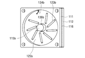
図10は、二個の筺体111,112間に挟まれたプリント配線板116に副線路123bが設けられたプリント配線板ビア・パターンコイル型方向性結合器であり、ケーブル孔136bに挿通された内部導体115bに流れる進行波の電流と反射波の電流とが副線路123bによって別々に検出される。符号124bは終端回路である。
しかしながら副線路123a、123bの周囲には誘電体となる基板材料があり特性を劣化させる原因の一つとなる。
FIG. 10 shows a printed wiring board via / pattern coil type directional coupler in which a
However, there is a substrate material to be a dielectric around the
基板材料で一般的に使われるFR4は吸水率・湿度・温度に依存して寸法変化・誘電率変化を起こし、プリント配線板のセンサ回路のインピーダンス変化を生じさせる。また大電力用途では非常に大きな温度変化にさらされることから、測定結果を安定化させる為にはより高価な基板材料を使用せざるを得なかった。 FR4 generally used as a substrate material causes dimensional change and dielectric constant change depending on water absorption, humidity and temperature, and causes impedance change of a sensor circuit of a printed wiring board. In addition, since high power applications are exposed to very large temperature changes, more expensive substrate materials have to be used to stabilize the measurement results.
なお、空芯の1ターン型コイル型電流センサ・方向性結合器は従来から存在するもの、例えば1MHz前後の低周波では、結合度を上げる為にセンサ形状が伝搬方向へ長くなりセンサの体積が大きくなる。 In addition, an air-core one-turn coil current sensor and directional coupler are conventionally used. For example, at low frequencies around 1 MHz, the sensor shape becomes longer in the propagation direction to increase the coupling degree, and the sensor volume is increased. growing.
本発明は上記温度変化があっても検出精度は低下しない技術を提供することにあり、検出レベル・検出位相が安定する小型方向性結合器を比較的安価に提供する。 The present invention is to provide a technology in which the detection accuracy does not decrease even if there is the above-mentioned temperature change, and provides a small directional coupler relatively stable in detection level and detection phase.
上記課題を解決するために、本発明は、プリント配線板と、前記プリント配線板に形成され、測定対象の導電線が挿通されるべきケーブル孔と、前記プリント配線板に設けられ、前記ケーブル孔に挿通された前記導電線に流れる進行波と反射波のいずれか一方を検出する第一の検出部と、他方を検出する第二の検出部とを有する方向性結合器であって、前記第一、第二の検出部は、中央に測定孔が位置する湾曲形状にされた複数の検出器と、前記検出器と検出器とを接続する複数の内部配線と、を有し、前記検出器の両端部のうち、一方の端部は前記測定孔の縁の近くに配置され他方の端部は前記一方の端部よりも前記縁から遠くに配置されて前記検出器同士は前記プリント配線板上に対面して立設され、前記第一、第二の検出部は、複数の前記検出器と複数の前記内部配線とによって形成された巻線を有し、前記第一の検出部の前記巻線を形成する前記検出器の前記測定孔と、前記第二の検出部の前記巻線を形成する前記検出器の前記測定孔とには、前記ケーブル孔に挿通された前記導電線に電流が流れたときに形成される磁束の少なくとも一部がそれぞれ貫通するように配置された方向性結合器である。
本発明は、前記内部配線は前記プリント配線板に形成された金属膜である方向性結合器である。
本発明は、前記ケーブル孔の中心を中心とする時計回りの方向と反時計回りの方向のいずれか一方を第一の配置方向としたときに、前記第一の検出部は、前記縁の近くに配置された前記端部が、前記第一の配置方向に隣接配置された前記検出器の前記縁から遠くに配置された前記端部に接続された前記検出器を有し、前記第一の配置方向と同じ方向又は逆の方向を第二の配置方向としたときに、前記第二の検出部は、前記縁の近くに配置された前記端部が、前記第二の配置方向に隣接配置された前記検出器の前記縁から遠くに配置された前記端部に接続された前記検出器を有する方向性結合器である。
本発明は、前記第一の検出部の前記検出器と前記第二の検出部の前記検出器とは、前記プリント配線板の同じ面に配置された方向性結合器である。
本発明は、前記第一の検出部の前記検出器と前記第二の検出部の前記検出器とは、前記プリント配線板の異なる面に配置された方向性結合器である。
本発明は、前記ケーブル孔に挿通された前記導電線を有する方向性結合器である。
本発明は、前記導電線には同軸ケーブルの内部導体が用いられた方向性結合器である。
In order to solve the above problems, according to the present invention, a printed wiring board, a cable hole formed in the printed wiring board and into which a conductive wire to be measured is to be inserted, and the cable hole provided in the printed wiring board A directional coupler comprising: a first detection unit for detecting either one of a traveling wave and a reflected wave flowing through the conductive wire inserted in the first and second detection units for detecting the other; The first and second detection units have a plurality of curved detectors each having a measurement hole at the center, and a plurality of internal wirings connecting the detectors and the detectors, and the detectors Among the two end portions, one end portion is disposed near the edge of the measurement hole, and the other end portion is disposed farther from the edge than the one end portion, and the detectors are connected to the printed wiring board The first and second detection units are erected facing each other on the plurality of The measurement hole of the detector which has a winding formed by the detector and the plurality of internal wirings and which forms the winding of the first detection unit; and the second detection unit In the measurement hole of the detector forming a winding, at least a part of the magnetic flux formed when the current flows through the conductive wire inserted in the cable hole is arranged to penetrate respectively It is a directional coupler.
The present invention is the directional coupler, wherein the internal wiring is a metal film formed on the printed wiring board.
In the present invention, the first detection portion is near the edge when one of a clockwise direction and a counterclockwise direction around the center of the cable hole is a first arrangement direction. The end located at the first end having the detector connected to the end located far from the edge of the detector located adjacent in the first disposition direction; When the second arrangement direction is the same as or opposite to the arrangement direction, the second detection unit may be arranged such that the end disposed near the edge is adjacent to the second arrangement direction. A directional coupler comprising the detector connected to the end remote from the edge of the detector.
In the present invention, the detector of the first detector and the detector of the second detector are directional couplers disposed on the same surface of the printed wiring board.
In the present invention, the detector of the first detection unit and the detector of the second detection unit are directional couplers disposed on different sides of the printed wiring board.
The present invention is a directional coupler having the conductive wire inserted into the cable hole.
The present invention is a directional coupler in which an inner conductor of a coaxial cable is used for the conductive wire.
温度の影響を受けない検出結果が得られる。 It is possible to obtain detection results that are not affected by temperature.
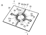
図1、図2を参照し、符号10aは本発明の第一例の方向性結合器であり、第一の筺体11と、第二の筺体12と、検出器本体16とを有している。
検出器本体16はプリント配線板25を有しており、プリント配線板25の中央位置にはプリント配線板25を貫通するケーブル孔36が設けられている。符号29は、方向性結合器10aを取りつけるための穴である。図1のプリント配線板25は、図2のプリント配線板25のA−A線截断断面図に相当する。
1 and 2,
The detector
方向性結合器10aの測定対象は、例えば高周波電圧を用いる装置に電力を供給するための同軸ケーブル等であり、同軸ケーブルは、一般に、接地電位に接続された筒状の外部導体と、外部導体とは絶縁された状態で外部導体の内部に挿通された太線状の内部導体とを有している。
An object to be measured of the
図1の符号15は、本発明の方向性結合器10aが測定対象とする導電線であり、ここでは同軸ケーブルの内部導体が導電線15としてケーブル孔36に挿通される。導電線は、同軸ケーブルの内部導体に限定されず、例えば平行な二本の電線のうち信号線を導電線として用いることができる。
ケーブル孔36の周囲に位置するプリント配線板25上には検出部20が配置されている。
検出部20には、導電線15中を一方向に流れる進行波電流と反対方向に流れる反射波電流のうち、いずれか一方の電流を検出する第一の検出部21aと、他方の電流を検出する第二の検出部22aとが設けられている。第一、第二の検出部21a、22aは、図4に示す複数の連結用電極部40と、複数の検出器23aとをそれぞれ有している。
A
In the
各検出器23aは同じ形状にされており、図3(a)は検出器23aの形状の一例である。この検出器23aは、後述する巻線の中の1ターンを構成する部品であり、一個の検出器23aは、両端が近接して離間した場所に位置するように湾曲した形状の一枚の金属板であり、その金属板の形状はU字形形状になっている。
Each
各検出器23aの中央には、検出器23aの金属板で囲まれる測定孔31がそれぞれ形成されている。検出器23aの中で湾曲された金属板の部分をループ部32と呼ぶと、ループ部32の一端と他端とには、ループ部32の外側に向けられた接続部33がそれぞれ設けられている。ここでは接続部33は、ループ部32の一端付近と他端付近とが折り曲げられて形成されている。
At the center of each
第一の検出部21aが有する複数の連結用電極部40と、第二の検出部22aが有する複数の連結用電極部40とは、ケーブル孔36の縁39に沿って配置されている。
連結用電極部40は、図4(a)に示すように、内側電極41と外側電極42と内部配線43とを有しており、内側電極41は縁39の近くに配置され、外側電極42は内側電極41よりも縁39から遠い位置に配置され、一個の内側電極41と一個の外側電極42とは一個の内部配線43によって接続されている。
The plurality of
The
ケーブル孔36の中心を中心とした時計回りと反時計回りの方向うち、いずれか一方を配置方向とすると、一個の連結用電極部40の外側電極42は、内側電極41に対して配置方向に離間しており、一個の連結用電極部40の内側電極41は、配置方向とは反対方向に隣接する連結用電極部40の外側電極42と縁39との間に配置されている。第一の検出部21aの配置方向と第二の検出部22aの配置方向は同一方向であっても互いに逆の方向であってもよい。
If one of the clockwise and counterclockwise directions about the center of the
ケーブル孔36は円形であり、内側電極41と外側電極42とはケーブル孔36の中心を中心とする円上に配置されており、一個の連結用電極部40の外側電極42と、配置方向に隣接する連結用電極部40の内側電極41とは、ケーブル孔36の中心を通る同じ放射線44上に位置している。
The
配置方向の始点となる連結用電極部40の内側電極41の外側には、第一の接続電極46が配置されており、他方、配置方向の終点となる連結用電極部40の外側電極42の内側には、第二の接続電極47が配置されている。従って、配置方向の始点となる連結用電極部40の内側電極41と第一の接続電極46とが同じ放射線44上に位置し、配置方向の終点となる連結用電極部40の外側電極42と第二の接続電極47とが同じ放射線44上に位置している。
第一の接続電極46には第一の外部配線27が接続され、第二の接続電極47には第二の外部配線28が接続されている。
The
A first
内側電極41と、外側電極42と、内部配線43と、第一、第二の外部配線27、28とは、数μm〜数百μmの金属膜で形成され、プリント配線板25に密着して固定されており、内側電極41と外側電極42との間に形成される寄生誘導性成分は小さくなるようにされている。
また、内側電極41と外側電極42との間は離間して配置されており、寄生容量性成分も小さくなるようにされている。
The
Further, the
各検出器23aはプリント配線板25に対して垂直にされ、同一の放射線44上に並んだ内側電極41と第一の接続電極46とには一個の検出器23aの二個の接続部33がそれぞれ一個ずつ接続されて固定されており、また、同一の放射線44上に並んだ第二の接続電極47と外側電極42とには、他の一個の検出器23aの二個の接続部33がそれぞれ一個ずつ接続されて固定されており、また、同一の放射線44上に並んだ内側電極41と外側電極42とには、他の一個の検出器23aの二個の接続部33がそれぞれ一個ずつ接続されて固定されている。
Each
この状態では、第一の検出部21aが有する検出器23aは、隣接する検出器23aの測定孔31が対面されて測定孔31が連通するように対面してプリント配線板25の同一面上に立設され、また、第二の検出部22aが有する検出器23aも、隣接する検出器23aの測定孔31が対面されて測定孔31が連通するように対面してプリント配線板25の同一面上に立設されており、各検出器23aは、プリント配線板25に固定されている。
In this state, the
各検出器23aの内側電極41に接続された部分を内側端、外側電極42に接続された部分を外側端とすると、プリント配線板25に設けられた内部配線43により、検出器23aの内側端は隣接する検出器23aの外側端に接続されており、各検出器23aのループ部32はプリント配線板25に立設されていることから、検出器23aと内部配線43とによって同じ方向に巻き回された螺旋状の巻線が形成されている。
Assuming that the portion connected to the
各検出器23aは、同じ巻線を構成する検出器23aの測定孔31が連通するように配置されており、連通する測定孔31によって巻線の空芯が形成されている。ケーブル孔36に挿入された内部導体から成る導電線15に電流が流れ、導電線15を中心とした円形の磁束が形成されると、その磁束の一部は空芯を構成する測定孔31を貫通し、磁束が貫通した測定孔31を有する各検出器23aに起電力が発生する。
The
同じ巻線の各検出器23aは、各検出器23aに発生した起電力が打ち消し合わずに加算されるように直列接続されており、増幅された各検出器23aの起電力を合計した合計起電力は第一の接続電極46と第二の接続電極47との間に現れる。
The
第一、第二の外部配線27、28はプリント配線板25上で延設され、一方の外部配線が電圧出力端子に接続され、他方の外部配線は終端回路24を介して接地電位に接続されている。第一の外部配線27は電圧端子に接続され、第二の外部配線28は終端回路24を介して接地電位に接続されており、接続された終端回路24の内部回路の構成によって、第一、第二の検出部21a、22aの一方が導電線15を流れる進行波を検出し、他方が導電線15を流れる反射波を検出し、進行波の大きさを示す信号と、反射波の大きさを示す信号とを別々の電圧端子から取り出せるようになっている。電圧端子の電圧が電圧端子に接続されたアナログICや作動増幅器等の検出装置によって取り出されると、進行波や反射波の大きさが求められ、求めた大きさをディスプレイ等に表示することができる。
上記の検出器23aは剛性を有する金属板によって構成されていることから、変形による電気的特性の変化が無いようになっている。
The first and second
Since the above-mentioned
従来技術では、プリント配線板の表面と裏面に形成した金属配線とスルーホールに充填した金属充填物とで、巻線を形成することができるが、その巻線の芯はプリント配線板を構成する樹脂になる。樹脂の誘電率は温度によって大きく変動するため、プリント配線板を芯にした巻線は電気特性が温度によって大きく変動する。
本発明の方向性結合器10aでは、検出器23aと内部配線43とで構成された巻線の芯は空気なので、巻線の電気特性は温度変化の影響を受けないで済む。
In the prior art, a winding can be formed by the metal wiring formed on the front and back of the printed wiring board and the metal filling filled in the through hole, but the core of the winding constitutes the printed wiring board Become a resin. Since the dielectric constant of the resin largely fluctuates depending on the temperature, the winding centered on the printed wiring board largely fluctuates in electrical characteristics depending on the temperature.
In the
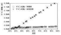
図7は、常温を基準としたときの、温度と検出信号ゲイン変動との関係を示すグラフであり、図8は、常温を基準としたときの、温度と検出信号フェーズ変動との関係を示すグラフである。 FIG. 7 is a graph showing the relationship between temperature and detection signal gain fluctuation when using normal temperature as a standard, and FIG. 8 shows the relationship between temperature and detection signal phase fluctuation when using normal temperature as a reference It is a graph.
図7、8から、検出信号ゲイン変動と検出信号フェーズ変動について、従来技術の方向性結合器の特性は温度の影響が大きいのに対し、本願発明の方向性結合器の特性は、温度変化による影響が無いと言える。 From FIGS. 7 and 8, the characteristics of the directional coupler of the prior art with respect to the detection signal gain fluctuation and the detection signal phase fluctuation are largely affected by the temperature, while the characteristics of the directional coupler of the present invention are due to the temperature change. It can be said that there is no effect.
以上説明した方向性結合器10aでは、第一の検出部21aと第二の検出部22aとがプリント配線板25の同じ面に配置されていたが、第一の検出部21aと第二の検出部22aとをプリント配線板25の異なる面に配置してもよい。
In the
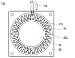
例えば、図5、図6の方向性結合器10bでは、第一の筺体11と第二の筺体12とに挟まれたプリント配線板25の片面に第一の検出部21bの検出器23aと、その検出器23a同士を接続する連結用電極部とが配置され、第一の検出部21bの検出器23aが配置された面とは反対側の面に第二の検出部22bの検出器23aと、その検出器23a同士を接続する連結用電極部とが配置されている。
For example, in the
このように配置した場合は、同じ面に第一、第二の検出部21a、22aを配置する場合に比べて第一、第二の検出部21b、22bに設ける検出器23aの個数を増加させることができるので、検出感度が向上する。
When arranged in this manner, the number of
なお、図4の連結用電極部40の配置方向は時計回りの方向であったが、終端回路24の内容により、第一の検出部21aの配置方向と第二の検出部22aの配置方向は同じ方向であってもよいし、互いに逆方向であってもよい。
Although the arrangement direction of the
また、上記検出器23aでは、接続部33は外側向きであったが、図3(b)のように、ループ部32の両端に内側向きの接続部34が設けられた検出器23bを用いることもできる。検出器23a、23bは、厚み0.1mm以上、幅0.3mm以上の金属板を曲げることにより巻線を構成させることができる。また、金属以外の電導体を用いることもできる。
Further, in the above-mentioned
なお、本発明の方向性結合器は導電線が設けられていてもよく、また、測定対象の内部導体等を導電線15とすることができるように、ケーブル孔36には導電線15を挿通させておかないようにしてもよい。
The directional coupler of the present invention may be provided with a conductive wire, and the
内蔵する本発明の方向性結合器によって測定した進行波・反射波を直流電圧に変換し、出力電圧の大きさを制御するRF電源装置が得られる。
内蔵する本発明の方向性結合器によって測定した進行波・反射波から有効電力、インピーダンスを算出し、所定の有効電力になるように周波数や進行波の大きさを変化させるRF電源装置が得られる。
An RF power supply device is obtained which converts the traveling wave / reflected wave measured by the directional coupler according to the present invention into a DC voltage and controls the magnitude of the output voltage.
It is possible to obtain an RF power supply device which calculates active power and impedance from traveling waves and reflected waves measured by the directional coupler of the present invention incorporated therein, and changes the frequency and the magnitude of traveling waves so as to obtain predetermined active power. .
内蔵する本発明の方向性結合器によって測定した進行波・反射波から反射係数を求め、可変リアクタンスを制御して反射係数をゼロにするマッチングボックスが得られる。 The reflection coefficient is determined from the traveling wave / reflected wave measured by the built-in directional coupler of the present invention, and a matching box is obtained which controls the variable reactance to make the reflection coefficient zero.
10a、10b……方向性結合器
15……導電線
21a、21b……第一の検出部
22a、22b……第二の検出部
23a、23b……検出器
25……プリント配線板
36……ケーブル孔
41……内側電極
42……外側電極
43……内部配線
10a, 10b ...
Claims (7)
前記プリント配線板に形成され、測定対象の導電線が挿通されるべきケーブル孔と、
前記プリント配線板に設けられ、前記ケーブル孔に挿通された前記導電線に流れる進行波と反射波のいずれか一方を検出する第一の検出部と、他方を検出する第二の検出部とを有する方向性結合器であって、
前記第一、第二の検出部は、中央に測定孔が位置する湾曲形状にされた複数の検出器と、
前記検出器と検出器とを接続する複数の内部配線と、を有し、
前記検出器の両端部のうち、一方の端部は前記測定孔の縁の近くに配置され他方の端部は前記一方の端部よりも前記縁から遠くに配置されて前記検出器同士は前記プリント配線板上に対面して立設され、
前記第一、第二の検出部は、複数の前記検出器と複数の前記内部配線とによって形成された巻線を有し、
前記第一の検出部の前記巻線を形成する前記検出器の前記測定孔と、前記第二の検出部の前記巻線を形成する前記検出器の前記測定孔とには、前記ケーブル孔に挿通された前記導電線に電流が流れたときに形成される磁束の少なくとも一部がそれぞれ貫通するように配置された方向性結合器。 Printed wiring board,
A cable hole which is formed on the printed wiring board and through which a conductive wire to be measured is to be inserted;
A first detection unit provided on the printed wiring board for detecting one of a traveling wave and a reflected wave flowing through the conductive wire inserted into the cable hole; and a second detection unit for detecting the other. A directional coupler having
The first and second detectors include a plurality of curved detectors each having a measurement hole at the center thereof;
A plurality of internal wires connecting the detector and the detector;
Among the both ends of the detector, one end is disposed near the edge of the measurement hole, and the other end is disposed farther from the edge than the one end, and the detectors are connected to each other. Set up facing the printed wiring board,
The first and second detection units have a winding formed by a plurality of the detectors and a plurality of the internal wirings,
The cable hole is formed in the measurement hole of the detector forming the winding of the first detection unit and the measurement hole of the detector forming the winding of the second detection unit. A directional coupler that is disposed such that at least a portion of the magnetic flux formed when an electric current flows through the inserted conductive wire.
Priority Applications (1)
| Application Number | Priority Date | Filing Date | Title |
|---|---|---|---|
| JP2017203732A JP7016238B2 (en) | 2017-10-20 | 2017-10-20 | Directional coupler |
Applications Claiming Priority (1)
| Application Number | Priority Date | Filing Date | Title |
|---|---|---|---|
| JP2017203732A JP7016238B2 (en) | 2017-10-20 | 2017-10-20 | Directional coupler |
Publications (2)
| Publication Number | Publication Date |
|---|---|
| JP2019078563A true JP2019078563A (en) | 2019-05-23 |
| JP7016238B2 JP7016238B2 (en) | 2022-02-04 |
Family
ID=66628741
Family Applications (1)
| Application Number | Title | Priority Date | Filing Date |
|---|---|---|---|
| JP2017203732A Active JP7016238B2 (en) | 2017-10-20 | 2017-10-20 | Directional coupler |
Country Status (1)
| Country | Link |
|---|---|
| JP (1) | JP7016238B2 (en) |
Cited By (5)
| Publication number | Priority date | Publication date | Assignee | Title |
|---|---|---|---|---|
| CN115656864A (en) * | 2022-09-09 | 2023-01-31 | 北京北方华创微电子装备有限公司 | A radio frequency power signal acquisition circuit and semiconductor process equipment |
| KR20230075809A (en) * | 2021-11-23 | 2023-05-31 | 한국교통대학교산학협력단 | A 3-Phase Current Detecting Device Using the Induction Coils |
| WO2023109676A1 (en) * | 2021-12-16 | 2023-06-22 | 华为技术有限公司 | Coupler and signal detection system |
| EP4411785A1 (en) * | 2023-02-06 | 2024-08-07 | Korea Institute of Fusion Energy | Module for measuring current/voltage/power of plasma apparatus and plasma apparatus including the same |
| KR20240178098A (en) * | 2023-06-21 | 2024-12-30 | 주식회사 뉴파워 프라즈마 | Radio frequency voltage current sensor |
Citations (6)
| Publication number | Priority date | Publication date | Assignee | Title |
|---|---|---|---|---|
| US4622558A (en) * | 1980-07-09 | 1986-11-11 | Corum Janes F | Toroidal antenna |
| JP2007201199A (en) * | 2006-01-26 | 2007-08-09 | Matsushita Electric Works Ltd | Toroidal coil structure |
| JP2010266233A (en) * | 2009-05-12 | 2010-11-25 | Murata Mfg Co Ltd | Device for detection of magnetic field |
| JP2012026780A (en) * | 2010-07-21 | 2012-02-09 | Daihen Corp | High-frequency detection device and coaxial tube provided with high-frequency detection device |
| WO2014203346A1 (en) * | 2013-06-19 | 2014-12-24 | ルネサスエレクトロニクス株式会社 | Power transmission device, wireless power feeding system, and control method |
| JP2015173189A (en) * | 2014-03-12 | 2015-10-01 | 株式会社村田製作所 | Coil device and manufacturing method of coil device |
-
2017
- 2017-10-20 JP JP2017203732A patent/JP7016238B2/en active Active
Patent Citations (6)
| Publication number | Priority date | Publication date | Assignee | Title |
|---|---|---|---|---|
| US4622558A (en) * | 1980-07-09 | 1986-11-11 | Corum Janes F | Toroidal antenna |
| JP2007201199A (en) * | 2006-01-26 | 2007-08-09 | Matsushita Electric Works Ltd | Toroidal coil structure |
| JP2010266233A (en) * | 2009-05-12 | 2010-11-25 | Murata Mfg Co Ltd | Device for detection of magnetic field |
| JP2012026780A (en) * | 2010-07-21 | 2012-02-09 | Daihen Corp | High-frequency detection device and coaxial tube provided with high-frequency detection device |
| WO2014203346A1 (en) * | 2013-06-19 | 2014-12-24 | ルネサスエレクトロニクス株式会社 | Power transmission device, wireless power feeding system, and control method |
| JP2015173189A (en) * | 2014-03-12 | 2015-10-01 | 株式会社村田製作所 | Coil device and manufacturing method of coil device |
Cited By (11)
| Publication number | Priority date | Publication date | Assignee | Title |
|---|---|---|---|---|
| KR20230075809A (en) * | 2021-11-23 | 2023-05-31 | 한국교통대학교산학협력단 | A 3-Phase Current Detecting Device Using the Induction Coils |
| KR102687202B1 (en) | 2021-11-23 | 2024-07-19 | 국립한국교통대학교산학협력단 | A 3-Phase Current Detecting Device Using the Induction Coils |
| WO2023109676A1 (en) * | 2021-12-16 | 2023-06-22 | 华为技术有限公司 | Coupler and signal detection system |
| CN115656864A (en) * | 2022-09-09 | 2023-01-31 | 北京北方华创微电子装备有限公司 | A radio frequency power signal acquisition circuit and semiconductor process equipment |
| CN115656864B (en) * | 2022-09-09 | 2024-03-26 | 北京北方华创微电子装备有限公司 | Radio frequency power supply signal acquisition circuit and semiconductor process equipment |
| EP4411785A1 (en) * | 2023-02-06 | 2024-08-07 | Korea Institute of Fusion Energy | Module for measuring current/voltage/power of plasma apparatus and plasma apparatus including the same |
| JP2024111819A (en) * | 2023-02-06 | 2024-08-19 | コリア インスティテュート オブ フュージョン エナジー | Current/voltage/power measurement module for plasma device and plasma device having same |
| JP7636597B2 (en) | 2023-02-06 | 2025-02-26 | コリア インスティテュート オブ フュージョン エナジー | Current/voltage/power measurement module for plasma device and plasma device having same |
| US12580167B2 (en) | 2023-02-06 | 2026-03-17 | Koreas Institute of Fusion Energy | Module for measuring current/voltage/power of plasma apparatus and plasma apparatus including the same |
| KR20240178098A (en) * | 2023-06-21 | 2024-12-30 | 주식회사 뉴파워 프라즈마 | Radio frequency voltage current sensor |
| KR102844445B1 (en) | 2023-06-21 | 2025-08-11 | 주식회사 뉴파워 프라즈마 | Radio frequency voltage current sensor |
Also Published As
| Publication number | Publication date |
|---|---|
| JP7016238B2 (en) | 2022-02-04 |
Similar Documents
| Publication | Publication Date | Title |
|---|---|---|
| JP7016238B2 (en) | Directional coupler | |
| US7714594B2 (en) | Current detection printed board, voltage detection printed board, and current/voltage detector using same, and current detector and voltage detector | |
| US7538562B2 (en) | High performance miniature RF sensor for use in microelectronics plasma processing tools | |
| JP5151032B2 (en) | Magnetic field probe device and magnetic field probe element | |
| KR101257980B1 (en) | Orthogonal radio frequency voltage/current sensor with high dynamic range | |
| KR20230027087A (en) | RF voltage and current (V-I) sensors and measurement methods | |
| US10545177B2 (en) | Non-contact sensor based Rogowski coil | |
| US10901005B2 (en) | Low power based Rogowski coil | |
| US6696834B2 (en) | Magnetic field probe having a shielding layer to protect lead wires with an isolating layer | |
| JP5418424B2 (en) | Electromagnetic field probe | |
| JP3583276B2 (en) | Near magnetic field probe, near magnetic field probe unit, near magnetic field probe array, and magnetic field measurement system | |
| CN105388352B (en) | B dot probes and electric current spatial distribution measuring system based on PCB formula magnetic induction coils | |
| US3829770A (en) | Directional coupler for transmission lines | |
| JP2010088011A (en) | Directional coupler | |
| US7482814B2 (en) | Electric/magnetic field sensor | |
| US11946953B2 (en) | Electromagnetic field sensor | |
| JP2000028661A (en) | Method and apparatus for measuring ground resistance | |
| JP6985317B2 (en) | Discharge measurement circuit | |
| JP2010081507A (en) | Directional coupler | |
| CN101405607A (en) | High performance miniature RF sensor for use in microelectronics plasma processing tools | |
| CN111610368A (en) | Impedance sensor and semiconductor device | |
| JP2012013582A (en) | Noise measurement cable and noise measurement device | |
| JP2009058384A (en) | Probe and apparatus for measuring intensity of electromagnetic field | |
| JPH1114679A (en) | High frequency current detector | |
| JP2014115133A (en) | Magnetic sensor and ampere meter |
Legal Events
| Date | Code | Title | Description |
|---|---|---|---|
| RD03 | Notification of appointment of power of attorney |
Free format text: JAPANESE INTERMEDIATE CODE: A7423 Effective date: 20200727 |
|
| RD04 | Notification of resignation of power of attorney |
Free format text: JAPANESE INTERMEDIATE CODE: A7424 Effective date: 20200805 |
|
| A621 | Written request for application examination |
Free format text: JAPANESE INTERMEDIATE CODE: A621 Effective date: 20200817 |
|
| A621 | Written request for application examination |
Free format text: JAPANESE INTERMEDIATE CODE: A621 Effective date: 20200817 |
|
| A131 | Notification of reasons for refusal |
Free format text: JAPANESE INTERMEDIATE CODE: A131 Effective date: 20211019 |
|
| A521 | Request for written amendment filed |
Free format text: JAPANESE INTERMEDIATE CODE: A523 Effective date: 20211220 |
|
| RD02 | Notification of acceptance of power of attorney |
Free format text: JAPANESE INTERMEDIATE CODE: A7422 Effective date: 20211220 |
|
| TRDD | Decision of grant or rejection written | ||
| A01 | Written decision to grant a patent or to grant a registration (utility model) |
Free format text: JAPANESE INTERMEDIATE CODE: A01 Effective date: 20220111 |
|
| A61 | First payment of annual fees (during grant procedure) |
Free format text: JAPANESE INTERMEDIATE CODE: A61 Effective date: 20220125 |
|
| R150 | Certificate of patent or registration of utility model |
Ref document number: 7016238 Country of ref document: JP Free format text: JAPANESE INTERMEDIATE CODE: R150 |
|
| R250 | Receipt of annual fees |
Free format text: JAPANESE INTERMEDIATE CODE: R250 |
|
| R250 | Receipt of annual fees |
Free format text: JAPANESE INTERMEDIATE CODE: R250 |