JP2019124792A - Display device - Google Patents
Display device Download PDFInfo
- Publication number
- JP2019124792A JP2019124792A JP2018004505A JP2018004505A JP2019124792A JP 2019124792 A JP2019124792 A JP 2019124792A JP 2018004505 A JP2018004505 A JP 2018004505A JP 2018004505 A JP2018004505 A JP 2018004505A JP 2019124792 A JP2019124792 A JP 2019124792A
- Authority
- JP
- Japan
- Prior art keywords
- wiring
- substrate
- sub
- display device
- partial
- Prior art date
- Legal status (The legal status is an assumption and is not a legal conclusion. Google has not performed a legal analysis and makes no representation as to the accuracy of the status listed.)
- Pending
Links
Images





Classifications
-
- G—PHYSICS
- G09—EDUCATION; CRYPTOGRAPHY; DISPLAY; ADVERTISING; SEALS
- G09G—ARRANGEMENTS OR CIRCUITS FOR CONTROL OF INDICATING DEVICES USING STATIC MEANS TO PRESENT VARIABLE INFORMATION
- G09G3/00—Control arrangements or circuits, of interest only in connection with visual indicators other than cathode-ray tubes
- G09G3/20—Control arrangements or circuits, of interest only in connection with visual indicators other than cathode-ray tubes for presentation of an assembly of a number of characters, e.g. a page, by composing the assembly by combination of individual elements arranged in a matrix no fixed position being assigned to or needed to be assigned to the individual characters or partial characters
- G09G3/22—Control arrangements or circuits, of interest only in connection with visual indicators other than cathode-ray tubes for presentation of an assembly of a number of characters, e.g. a page, by composing the assembly by combination of individual elements arranged in a matrix no fixed position being assigned to or needed to be assigned to the individual characters or partial characters using controlled light sources
- G09G3/30—Control arrangements or circuits, of interest only in connection with visual indicators other than cathode-ray tubes for presentation of an assembly of a number of characters, e.g. a page, by composing the assembly by combination of individual elements arranged in a matrix no fixed position being assigned to or needed to be assigned to the individual characters or partial characters using controlled light sources using electroluminescent panels
- G09G3/32—Control arrangements or circuits, of interest only in connection with visual indicators other than cathode-ray tubes for presentation of an assembly of a number of characters, e.g. a page, by composing the assembly by combination of individual elements arranged in a matrix no fixed position being assigned to or needed to be assigned to the individual characters or partial characters using controlled light sources using electroluminescent panels semiconductive, e.g. using light-emitting diodes [LED]
- G09G3/3208—Control arrangements or circuits, of interest only in connection with visual indicators other than cathode-ray tubes for presentation of an assembly of a number of characters, e.g. a page, by composing the assembly by combination of individual elements arranged in a matrix no fixed position being assigned to or needed to be assigned to the individual characters or partial characters using controlled light sources using electroluminescent panels semiconductive, e.g. using light-emitting diodes [LED] organic, e.g. using organic light-emitting diodes [OLED]
- G09G3/3225—Control arrangements or circuits, of interest only in connection with visual indicators other than cathode-ray tubes for presentation of an assembly of a number of characters, e.g. a page, by composing the assembly by combination of individual elements arranged in a matrix no fixed position being assigned to or needed to be assigned to the individual characters or partial characters using controlled light sources using electroluminescent panels semiconductive, e.g. using light-emitting diodes [LED] organic, e.g. using organic light-emitting diodes [OLED] using an active matrix
-
- G—PHYSICS
- G09—EDUCATION; CRYPTOGRAPHY; DISPLAY; ADVERTISING; SEALS
- G09G—ARRANGEMENTS OR CIRCUITS FOR CONTROL OF INDICATING DEVICES USING STATIC MEANS TO PRESENT VARIABLE INFORMATION
- G09G3/00—Control arrangements or circuits, of interest only in connection with visual indicators other than cathode-ray tubes
- G09G3/20—Control arrangements or circuits, of interest only in connection with visual indicators other than cathode-ray tubes for presentation of an assembly of a number of characters, e.g. a page, by composing the assembly by combination of individual elements arranged in a matrix no fixed position being assigned to or needed to be assigned to the individual characters or partial characters
- G09G3/22—Control arrangements or circuits, of interest only in connection with visual indicators other than cathode-ray tubes for presentation of an assembly of a number of characters, e.g. a page, by composing the assembly by combination of individual elements arranged in a matrix no fixed position being assigned to or needed to be assigned to the individual characters or partial characters using controlled light sources
- G09G3/30—Control arrangements or circuits, of interest only in connection with visual indicators other than cathode-ray tubes for presentation of an assembly of a number of characters, e.g. a page, by composing the assembly by combination of individual elements arranged in a matrix no fixed position being assigned to or needed to be assigned to the individual characters or partial characters using controlled light sources using electroluminescent panels
- G09G3/32—Control arrangements or circuits, of interest only in connection with visual indicators other than cathode-ray tubes for presentation of an assembly of a number of characters, e.g. a page, by composing the assembly by combination of individual elements arranged in a matrix no fixed position being assigned to or needed to be assigned to the individual characters or partial characters using controlled light sources using electroluminescent panels semiconductive, e.g. using light-emitting diodes [LED]
- G09G3/3208—Control arrangements or circuits, of interest only in connection with visual indicators other than cathode-ray tubes for presentation of an assembly of a number of characters, e.g. a page, by composing the assembly by combination of individual elements arranged in a matrix no fixed position being assigned to or needed to be assigned to the individual characters or partial characters using controlled light sources using electroluminescent panels semiconductive, e.g. using light-emitting diodes [LED] organic, e.g. using organic light-emitting diodes [OLED]
- G09G3/3225—Control arrangements or circuits, of interest only in connection with visual indicators other than cathode-ray tubes for presentation of an assembly of a number of characters, e.g. a page, by composing the assembly by combination of individual elements arranged in a matrix no fixed position being assigned to or needed to be assigned to the individual characters or partial characters using controlled light sources using electroluminescent panels semiconductive, e.g. using light-emitting diodes [LED] organic, e.g. using organic light-emitting diodes [OLED] using an active matrix
- G09G3/3258—Control arrangements or circuits, of interest only in connection with visual indicators other than cathode-ray tubes for presentation of an assembly of a number of characters, e.g. a page, by composing the assembly by combination of individual elements arranged in a matrix no fixed position being assigned to or needed to be assigned to the individual characters or partial characters using controlled light sources using electroluminescent panels semiconductive, e.g. using light-emitting diodes [LED] organic, e.g. using organic light-emitting diodes [OLED] using an active matrix with pixel circuitry controlling the voltage across the light-emitting element
-
- H—ELECTRICITY
- H10—SEMICONDUCTOR DEVICES; ELECTRIC SOLID-STATE DEVICES NOT OTHERWISE PROVIDED FOR
- H10K—ORGANIC ELECTRIC SOLID-STATE DEVICES
- H10K50/00—Organic light-emitting devices
- H10K50/80—Constructional details
- H10K50/84—Passivation; Containers; Encapsulations
- H10K50/844—Encapsulations
-
- H—ELECTRICITY
- H10—SEMICONDUCTOR DEVICES; ELECTRIC SOLID-STATE DEVICES NOT OTHERWISE PROVIDED FOR
- H10K—ORGANIC ELECTRIC SOLID-STATE DEVICES
- H10K59/00—Integrated devices, or assemblies of multiple devices, comprising at least one organic light-emitting element covered by group H10K50/00
- H10K59/10—OLED displays
- H10K59/12—Active-matrix OLED [AMOLED] displays
- H10K59/127—Active-matrix OLED [AMOLED] displays comprising two substrates, e.g. display comprising OLED array and TFT driving circuitry on different substrates
-
- H—ELECTRICITY
- H10—SEMICONDUCTOR DEVICES; ELECTRIC SOLID-STATE DEVICES NOT OTHERWISE PROVIDED FOR
- H10K—ORGANIC ELECTRIC SOLID-STATE DEVICES
- H10K59/00—Integrated devices, or assemblies of multiple devices, comprising at least one organic light-emitting element covered by group H10K50/00
- H10K59/10—OLED displays
- H10K59/12—Active-matrix OLED [AMOLED] displays
- H10K59/131—Interconnections, e.g. wiring lines or terminals
-
- H—ELECTRICITY
- H10—SEMICONDUCTOR DEVICES; ELECTRIC SOLID-STATE DEVICES NOT OTHERWISE PROVIDED FOR
- H10K—ORGANIC ELECTRIC SOLID-STATE DEVICES
- H10K77/00—Constructional details of devices covered by this subclass and not covered by groups H10K10/80, H10K30/80, H10K50/80 or H10K59/80
- H10K77/10—Substrates, e.g. flexible substrates
- H10K77/111—Flexible substrates
-
- G—PHYSICS
- G09—EDUCATION; CRYPTOGRAPHY; DISPLAY; ADVERTISING; SEALS
- G09G—ARRANGEMENTS OR CIRCUITS FOR CONTROL OF INDICATING DEVICES USING STATIC MEANS TO PRESENT VARIABLE INFORMATION
- G09G2300/00—Aspects of the constitution of display devices
- G09G2300/04—Structural and physical details of display devices
- G09G2300/0421—Structural details of the set of electrodes
- G09G2300/0426—Layout of electrodes and connections
-
- G—PHYSICS
- G09—EDUCATION; CRYPTOGRAPHY; DISPLAY; ADVERTISING; SEALS
- G09G—ARRANGEMENTS OR CIRCUITS FOR CONTROL OF INDICATING DEVICES USING STATIC MEANS TO PRESENT VARIABLE INFORMATION
- G09G2330/00—Aspects of power supply; Aspects of display protection and defect management
- G09G2330/08—Fault-tolerant or redundant circuits, or circuits in which repair of defects is prepared
-
- H—ELECTRICITY
- H10—SEMICONDUCTOR DEVICES; ELECTRIC SOLID-STATE DEVICES NOT OTHERWISE PROVIDED FOR
- H10K—ORGANIC ELECTRIC SOLID-STATE DEVICES
- H10K2102/00—Constructional details relating to the organic devices covered by this subclass
- H10K2102/301—Details of OLEDs
- H10K2102/311—Flexible OLED
-
- H—ELECTRICITY
- H10—SEMICONDUCTOR DEVICES; ELECTRIC SOLID-STATE DEVICES NOT OTHERWISE PROVIDED FOR
- H10K—ORGANIC ELECTRIC SOLID-STATE DEVICES
- H10K59/00—Integrated devices, or assemblies of multiple devices, comprising at least one organic light-emitting element covered by group H10K50/00
- H10K59/80—Constructional details
- H10K59/87—Passivation; Containers; Encapsulations
- H10K59/873—Encapsulations
-
- Y—GENERAL TAGGING OF NEW TECHNOLOGICAL DEVELOPMENTS; GENERAL TAGGING OF CROSS-SECTIONAL TECHNOLOGIES SPANNING OVER SEVERAL SECTIONS OF THE IPC; TECHNICAL SUBJECTS COVERED BY FORMER USPC CROSS-REFERENCE ART COLLECTIONS [XRACs] AND DIGESTS
- Y02—TECHNOLOGIES OR APPLICATIONS FOR MITIGATION OR ADAPTATION AGAINST CLIMATE CHANGE
- Y02E—REDUCTION OF GREENHOUSE GAS [GHG] EMISSIONS, RELATED TO ENERGY GENERATION, TRANSMISSION OR DISTRIBUTION
- Y02E10/00—Energy generation through renewable energy sources
- Y02E10/50—Photovoltaic [PV] energy
- Y02E10/549—Organic PV cells
Landscapes
- Engineering & Computer Science (AREA)
- Physics & Mathematics (AREA)
- Computer Hardware Design (AREA)
- General Physics & Mathematics (AREA)
- Theoretical Computer Science (AREA)
- Microelectronics & Electronic Packaging (AREA)
- Optics & Photonics (AREA)
- Electroluminescent Light Sources (AREA)
- Devices For Indicating Variable Information By Combining Individual Elements (AREA)
- Liquid Crystal (AREA)
Abstract
Description
本発明の実施形態は、表示装置に関する。 Embodiments of the present invention relate to a display device.
携帯電話やPDA(personal digital assistant)等に用いられる表示装置では、性能面やデザイン性等の観点から、狭額縁化が要求されている。狭額縁化の一例として、ドライバなどが表示面の下側に位置するように、表示パネルの一部を折り曲げる方法が知られている。しかしながら、折り曲げられた領域に設けられた配線は、折り曲げによる応力の影響を受けて断線する場合がある。また、配線が断線した場合、配線全体の抵抗値が上昇し、配線に供給される信号が劣化するおそれがある。 In display devices used for mobile phones, PDAs (personal digital assistants), etc., narrowing of the frame is required from the viewpoint of performance and design. As an example of narrowing the frame, a method is known in which a part of the display panel is bent so that a driver or the like is located below the display surface. However, the wiring provided in the bent region may be broken due to the influence of the stress due to the bending. In addition, when the wiring is disconnected, the resistance value of the entire wiring is increased, and the signal supplied to the wiring may be deteriorated.
本実施形態の目的は、信頼性を向上することが可能な表示装置を提供することにある。 An object of the present embodiment is to provide a display device capable of improving the reliability.
一実施形態によれば、
基板と、前記基板に設けられた表示素子と、前記基板に設けられ、前記表示素子を駆動する駆動部と、前記表示素子と電気的に接続された第1配線と、を備え、前記第1配線は、第1方向に突出した第1屈曲部と、前記第1方向の逆方向に突出した第2屈曲部とを有し、前記第1方向、及び前記第1方向と交差する第2方向において、前記第1屈曲部の第1位置と前記第2屈曲部の第2位置とは、異なっている、表示装置が提供される。
According to one embodiment,
A substrate, a display element provided on the substrate, a drive unit provided on the substrate for driving the display element, and a first wiring electrically connected to the display element; The wiring has a first bending portion protruding in a first direction and a second bending portion protruding in a direction opposite to the first direction, and a second direction intersecting the first direction and the first direction. In the display device, the first position of the first bend and the second position of the second bend may be different.
一実施形態によれば、
基板と、前記基板に設けられた表示素子と、前記基板に設けられ、前記表示素子を駆動する駆動部と、前記表示素子と前記駆動部とを電気的に接続する第2配線及び第3配線と、を備え、前記第2配線と前記第3配線とは、第1方向に沿って隣り合い、前記第2配線は、第4屈曲部を有し、前記第3配線は、第5屈曲部を有し、前記第1方向と交差する第2方向において、前記第4屈曲部の第6位置と前記第5屈曲部の第7位置とは、異なっている、表示装置が提供される。
According to one embodiment,
A substrate, a display element provided on the substrate, a drive unit provided on the substrate and driving the display element, and second and third wirings electrically connecting the display element and the drive unit And the second wiring and the third wiring are adjacent to each other along the first direction, the second wiring has a fourth bent portion, and the third wiring is a fifth bent portion. A display device is provided, wherein the sixth position of the fourth bent portion and the seventh position of the fifth bent portion are different in a second direction intersecting the first direction.
以下、本実施形態について、図面を参照しながら説明する。なお、開示はあくまで一例に過ぎず、当業者において、発明の主旨を保っての適宜変更について容易に想到し得るものについては、当然に本発明の範囲に含有されるものである。また、図面は、説明をより明確にするため、実際の態様に比べて、各部の幅、厚さ、形状等について模式的に表される場合があるが、あくまで一例であって、本発明の解釈を限定するものではない。また、本明細書と各図において、既出の図に関して前述したものと同一又は類似した機能を発揮する構成要素には同一の参照符号を付し、重複する詳細な説明を適宜省略することがある。 Hereinafter, the present embodiment will be described with reference to the drawings. The disclosure is merely an example, and it is naturally included within the scope of the present invention as to what can be easily conceived of by those skilled in the art as to appropriate changes while maintaining the gist of the invention. In addition, the drawings may be schematically represented as to the width, thickness, shape, etc. of each portion as compared with the actual embodiment in order to clarify the description, but this is merely an example, and the present invention It does not limit the interpretation. In the specification and the drawings, components having the same or similar functions as those described above with reference to the drawings already described may be denoted by the same reference symbols, and overlapping detailed descriptions may be omitted as appropriate. .
[第1実施形態]
図1は、第1実施形態の表示装置DSPを概略的に示す斜視図である。図1は、表示装置DSPを部分的に分解して示している。
First Embodiment
FIG. 1 is a perspective view schematically showing a display device DSP of the first embodiment. FIG. 1 shows the display device DSP partially disassembled.
図において、方向X(第1方向)及び方向Y(第2方向)は、互いに交差する方向であり、方向Zは、方向X及び方向Yと交差する方向である。一例では、方向X、方向Y、及び方向Zは、互いに直交しているが、互いに90度以外の角度で交差していてもよい。本明細書において、方向Zを示す矢印の先端に向かう方向を上方(あるいは単に上)と称し、矢印の先端から逆に向かう方向を下方(あるいは単に下)と称する。また、方向Zを示す矢印の先端側に表示装置DSPを観察する観察一があるものとし、この観察位置から方向X及び方向Yで規定されるX−Y平面に向かって見ることを平面視という。 In the figure, the direction X (first direction) and the direction Y (second direction) are directions intersecting each other, and the direction Z is a direction intersecting the directions X and Y. In one example, the direction X, the direction Y, and the direction Z are orthogonal to each other, but may intersect each other at an angle other than 90 degrees. In the present specification, the direction toward the tip of the arrow indicating the direction Z is referred to as upward (or simply upward), and the direction opposite to the tip of the arrow is referred to as downward (or simply downward). In addition, it is assumed that there is an observation side for observing the display device DSP on the tip side of the arrow indicating the direction Z, and viewing from this observation position toward the XY plane defined by the direction X and the direction Y is referred to as a plan view. .
本実施形態において、表示装置DSPは、一例として、有機エレクトロルミネッセンス(EL)素子を有する有機EL表示装置である。しかしながら、表示装置DSPは、液晶層を有する液晶表示装置、電気泳動型素子等を有する電子ペーパー型表示装置等、他の表示装置であってもよい。 In the present embodiment, the display device DSP is, for example, an organic EL display device having an organic electroluminescence (EL) element. However, the display device DSP may be another display device such as a liquid crystal display device having a liquid crystal layer, an electronic paper type display device having an electrophoretic element, or the like.
表示装置DSPは、基板1、ドライバ2、配線部3、カバー部材4、及び偏光板5備えている。
The display device DSP includes a
基板1は、可撓性を有し、一部が折り曲げられている。基板1は、一例では、平面状の平面領域PAと、曲面状の曲面領域CAとを有している。平面領域PAは、平面領域PA1とPA2を含み、平面領域PA1と平面領域PA2は、互いに対向している。曲面領域CAは、基板1が曲率を有する領域であり、平面領域PA1と平面領域PA2との間に位置している。図示した例では、曲面領域CAは、方向Xに沿った母線GLを有している。
The
複数の画素PXは、基板1に配置されている。複数の画素PXは、基板1の第1領域(例えば、平面領域PA1)に配置される。画素PXは、表示素子としての有機EL素子、有機EL素子に接続されたスイッチング素子などを含んでいる。
The plurality of pixels PX are disposed on the
ドライバ2は、基板1に実装されている。ドライバ2は、基板1の第3領域(例えば、平面領域PA2)に配置される。ドライバ2は、画素PXを駆動するための各種信号を供給する。
The driver 2 is mounted on the
配線部3は、基板1に配置されている。配線部3は、少なくとも第2領域(例えば、曲面領域CA)に位置している。第2領域は、第1領域及び第3領域の間に位置している。配線部3は、画素PXと電気的に接続された複数の配線を含んでいる。すなわち、配線部3は、画素PXとドライバ2とを電気的に接続するための配線や、画素PXに電源電位を供給するための配線などを備えている。
The
カバー部材4は、樹脂又はガラスなどの透明な材料で形成されている。カバー部材4は、平面領域PAのすべてを覆っている。偏光板5は、カバー部材4とほぼ同じ大きさであり、カバー部材4の直下に位置している。偏光板5は、例えば平面領域PAに配置された金属配線による反射光が視認されることを抑制する。なお、偏光板5は、省略されてもよい。
The
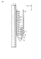
図2は、図1に示す表示装置DSPの構成例を示す断面図である。図2は、方向Y及び方向Zによって規定されるY−Z平面と平行な面を示している。図示した例では、基板1と偏光板5とは、接着剤6によって接着されている。
FIG. 2 is a cross-sectional view showing a configuration example of the display device DSP shown in FIG. FIG. 2 shows a plane parallel to the YZ plane defined by the directions Y and Z. In the illustrated example, the
表示装置DSPは、基板1、ドライバ2、配線部3、カバー部材4、及び偏光板5に加え、支持部材71及び72を備えている。
The display device DSP includes
基板1は、副基板(第1副基板)101と副基板(第2副基板)102とを含んでいる。副基板101は、副基板102よりも上方に位置し、接着剤6と接している。図示した例では、副基板101は、平面領域PA1と曲面領域CAの双方を備えている。副基板101及び副基板102は、平面領域PA2を備えている。副基板102は、副基板101の平面領域PA1の下方に位置している。副基板102は、一例では、フレキシブル回路基板(FPC)である。副基板102は、副基板101の一端部に接続される。副基板102は、例えば異方性導電膜を介して副基板101と電気的に接続されている。
The
支持部材71と支持部材72は、副基板101に貼り付けられ、それぞれ平面領域PA1と平面領域PA2とを形成している。支持部材71と支持部材72とは、互いに対向している。
The
ドライバ2は、平面領域PA2に位置している。図示した例では、ドライバ2は、平面領域PA2において、副基板101のカバー部材4側の面と反対側の面に設けられている。
The driver 2 is located in the plane area PA2. In the illustrated example, the driver 2 is provided on the surface of the
本実施形態において、曲面領域CAは、副基板101が折り曲げ軸AXを中心に折り曲げられることで形成されている。ここで、折り曲げ軸AXは、方向Xと平行である。また、図において曲線の矢印で示すように、曲面領域CAに沿って平面領域PA1から平面領域PA2に向かう方向を、周方向Cと定義する。 In the present embodiment, the curved surface area CA is formed by bending the sub-substrate 101 around the bending axis AX. Here, the bending axis AX is parallel to the direction X. Further, as shown by a curved arrow in the figure, a direction from the plane area PA1 to the plane area PA2 along the curved area CA is defined as a circumferential direction C.
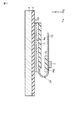
図3は、図1に示す表示装置DSPの他の構成例を示す断面図である。図3は、副基板102が曲面領域CAを有している点で、図2に示す例と相違している。 FIG. 3 is a cross-sectional view showing another configuration example of the display device DSP shown in FIG. FIG. 3 is different from the example shown in FIG. 2 in that the sub-substrate 102 has a curved surface area CA.
支持部材71は、副基板101に貼り付けられ、平面領域PA1を形成している。支持部材72は、副基板102に貼り付けられ、平面領域PA2を形成している。ドライバ2は、副基板102に実装されている。図示した例では、副基板102は、副基板101の一端部において、副基板101の下面、すなわちカバー部材4側の面と反対側の面に接続されている。なお、副基板102は、副基板101の上面に接続されていてもよい。
The
図4は、図1に示す配線部3の一部を示す図である。図4は、配線部3が備える配線31、32、及び33を示している。ここでは、形式的に、X−Y平面と平行な面を示している。なお、曲面領域CAにおいて、方向Yは、上述の周方向Cに相当する。
FIG. 4 is a view showing a part of the
配線31、32、及び33は、この順で方向Xに沿って並び、各々が方向Y(曲面領域CAにおいては周方向C)に延伸している。図示した例では、配線31、32、及び33の一端には、端子T11、T12、及びT13がそれぞれ設けられている。配線31、32、及び33の他端には、端子T21、T22、及びT23がそれぞれ設けられている。端子T11、T12、T13は、画素PXを駆動するための走査線、信号線、共通電極、電源電位供給配線(アノード電源配線、カソード電源配線)などに接続される。端子T21、T22、及びT23は、例えば上述のドライバ2に接続される。配線31、32、及び33には、それぞれ異なる信号が供給される。なお、配線31、32、及び33には、同一の信号が供給されてもよい。
The
ここで、配線31が配置される領域を配線領域WA1とする。図4に示す例では、配線領域WA1を長方形で示している。配線領域WA1は、配線31の延在方向(方向Y)に延びる中央線CL1で第1配線領域WLA1と第2配線領域WRA1に分けられる。また、配線領域WA1の配線31の延在方向と交差する方向における一方の端部を第1配線端部WLE1とし、他方の端部を第2配線端部WRE1とすると、第1配線端部WLE1から中央線CL1に向かう方向が方向X(方向Xの順方向)であり、第2配線端部WRE1から中央線CL1に向かう方向が方向Xの逆方向である。
Here, a region where the
配線31は、ジグザグ状に形成されている。すなわち、配線31は、複数の屈曲部31aと複数の屈曲部31bとを備えている。屈曲部(第4屈曲部)31aは、方向X(順方向)に向かって突出している。一方、屈曲部31bは、方向Xと逆方向に突出している。屈曲部31aは、第1角度θ1を有し、屈曲部31bは第2角度θ2を有する。第1角度θ1と第2角度θ2は、図示した例では、約90度であるが、少なくとも180より小さければよい。また、第1角度θ1と第2角度θ2は異なる角度であってもよい。さらに、屈曲部31aが複数ある場合は、屈曲部31aの第1角度θ1は一定でなくてもよく、異なる複数の角度を有してもよい。また、屈曲部31bが複数ある場合は、屈曲部31bの第2角度θ2は一定でなくてもよく、異なる複数の角度を有してもよい。また、屈曲部31aと屈曲部31bとは、方向Yに沿って交互に並んでいる。
The
配線32及び33は、配線31と同様の構造を有している。すなわち、配線32は、方向Xに突出した屈曲部(第5屈曲部)32aと、方向Xと逆方向に突出した屈曲部32bとを有している。配線33は、方向Xに突出した屈曲部33aと、方向Xと逆方向に突出した屈曲部33bとを有している。
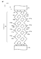
The
本実施形態において、少なくとも隣り合う配線は、屈曲部の位置が一致しないように配置されている。図示した例では、方向Yにおいて、屈曲部31aの位置(第6位置)、屈曲部32aの位置(第7位置)、及び屈曲部33aの位置は、互いに異なっている。換言すると、屈曲部31a、32a、及び33aは、方向Xに沿って並んでいない。ここで、屈曲部31aの位置は、屈曲部31aが有する頂点(第3頂点)P1aの位置に相当する。屈曲部32aの位置は、屈曲部32aが有する頂点(第4頂点)P2aの位置に相当する。屈曲部33aの位置は、屈曲部33aが有する頂点P3aの位置に相当する。
In the present embodiment, at least adjacent wires are arranged such that the positions of the bent portions do not coincide. In the illustrated example, in the direction Y, the position of the bending
同様に、方向Yにおける屈曲部31b、32b、及び33bの位置は、互いに異なっている。換言すると、屈曲部31b、32b、及び33bは、方向Xに沿って並んでいない。ここで、屈曲部31bの位置は、屈曲部31bが有する頂点P1bの位置に相当する。屈曲部32bの位置は、屈曲部32bが有する頂点P2bの位置に相当する。屈曲部33bの位置は、屈曲部33bが有する頂点P3bの位置に相当する。
Similarly, the positions of the
さらに、図示した例では、方向Yにおける屈曲部31aの位置は、方向Yにおける屈曲部32b及び33bの位置とも異なっている。同様に、方向Yにおける屈曲部32aの位置は、方向Yにおける屈曲部31b及び33bの位置とも異なっている。方向Yにおける屈曲部33aの位置は、方向Yにおける屈曲部31b及び32bの位置とも異なっている。
Furthermore, in the illustrated example, the position of the bending
本実施形態によれば、複数の配線31、32、及び33の間で方向Yにおける屈曲部の位置をずらすことによって、副基板101が折り曲げられたことによって生じる応力を分散させることができる。
According to the present embodiment, by shifting the position of the bent portion in the direction Y among the plurality of
ここでは、図10を参照して、その理由を説明する。図10は、比較例としての配線LEを示している。配線LEは、部分配線LE1、LE2、及びLE3を備えている。部分配線LE1、LE2、及びLE3は、方向Xに突出した屈曲部L1a、L2a、及びL3aと、方向Xと逆方向に突出したL1b、L2b、及びL3bをそれぞれ有している。例えば、図10に示すように、部分配線LE1、LE2、及びLE3の屈曲部L1a、L2a、及びL3aの方向Yにおける位置が揃っている場合、破線で示すように、屈曲部L1a、L2a、及びL3aの頂点を結ぶ直線上に応力が集中する傾向がある。また、屈曲部L1b、L2b、及びL3bの方向Yにおける位置が揃っている場合、破線で示すように、屈曲部L1b、L2b、及びL3bの頂点を結ぶ直線上に応力が集中する傾向がある。 Here, the reason will be described with reference to FIG. FIG. 10 shows a wiring LE as a comparative example. The wiring LE includes partial wirings LE1, LE2, and LE3. The partial wires LE1, LE2, and LE3 respectively include bent portions L1a, L2a, and L3a protruding in the direction X, and L1b, L2b, and L3b protruding in the direction opposite to the direction X. For example, as shown in FIG. 10, when the positions of partial interconnections LE1, LE2, and LE3 in bent portions L1a, L2a, and L3a in the direction Y are aligned, as shown by broken lines, bent portions L1a, L2a, and Stress tends to concentrate on the straight line connecting the tops of L3a. In addition, when the positions in the direction Y of the bent portions L1b, L2b, and L3b are aligned, stress tends to be concentrated on a straight line connecting the apexes of the bent portions L1b, L2b, and L3b, as indicated by the broken line.
一方、本実施形態では、屈曲部の方向Yにおける位置をずらすことによって、基板1の全体として応力が所定の領域に集中することを抑制することができ、曲面領域CAにおける曲率を均一にすることがでる。この結果、配線31、32、及び33の断線を抑制することができ、信頼性を向上することが可能な表示装置を提供することができる。
On the other hand, in the present embodiment, by shifting the position in the direction Y of the bent portion, it is possible to suppress concentration of stress on a predetermined region as a whole of the
[第2実施形態]
図5は、第2実施形態に係る表示装置DSPの配線31を示す図である。第2実施形態は、配線31が複数の部分配線(部分領域)を有している点で、第1実施形態と相違している。図5においては、配線31は、部分配線として部分配線(第1部分配線)311及び部分配線(第2部分配線)312を有する。
Second Embodiment
FIG. 5 is a view showing the
部分配線311と部分配線312とは、図4に示す配線31と同様の構造を有している。すなわち、部分配線311は、方向Xに突出した屈曲部(第1屈曲部)311aと、方向Xと逆方向に突出した屈曲部311bとを有している。屈曲部311aと311bとは、方向Yに(曲面領域CAにおいては周方向Cに)交互に並んでいる。部分配線312は、方向Xに突出した屈曲部312aと、方向Xと逆方向に突出した屈曲部(第2屈曲部)312bとを有している。屈曲部312aと屈曲部312bとは、方向Yに(曲面領域CAにおいては周方向Cに)交互に並んでいる。図示した例では、屈曲部311aと屈曲部312bとは、互いに逆方向に向かって突出している。また、屈曲部311bと屈曲部312aとは、互いに逆方向に向かって突出している。
The
本実施形態において、配線31に含まれる屈曲部の位置は、隣り合う屈曲部のうち少なくとも反対方向に突出した屈曲部の位置とは、方向X及び方向Yの双方において異なる。例えば、屈曲部311aの位置(第1位置)と屈曲部312bの位置(第2位置)とは、方向X及び方向Yの双方において異なっている。換言すると、屈曲部311aと屈曲部312bとは、方向Yに沿って並んでいない。また、屈曲部311aと屈曲部312bとは、方向Xに沿って並んでいない。ここで、屈曲部311aの位置とは、屈曲部311aが有する頂点(第1頂点)P11aの位置に相当する。また、屈曲部312bの位置とは、屈曲部312bが有する頂点(第2頂点)P12bの位置に相当する。
In the present embodiment, the position of the bent portion included in the
部分配線311と部分配線312とは、接続部CN(CN1、CN2)において接続(交差)されている。これにより、部分配線311と部分配線312とは、同電位である。つまり、部分配線311と部分配線312とには、同一の信号が供給される。このような配線31には、一例では、電源電位が供給される。部分配線(部分配線311、312)は、それぞれ異なる層に形成され、接続部CNを介して接続されてもよいが、部分配線、及び、接続部CNがいずれも同一の層で形成されてもよい。
The
隣り合う接続部(第1接続部)CN1の位置(第3位置)と接続部(第2接続部)CN2の位置(第4位置)とは、方向X及び方向Yの双方において異なっている。換言すると、接続部CN1と接続部CN2とは、方向Yに沿って並んでいない。また、接続部CN1と接続部CN2とは、方向Xに沿って並んでいない。屈曲部311aと屈曲部312bとは、接続部CN1と接続部CN2との間に位置し、互いに離間している。すなわち、配線31は、屈曲部311a、屈曲部312b、接続部CN1、及び接続部CN2の内周によって規定される開口OPを有している。
The position (third position) of the adjacent connection portion (first connection portion) CN1 and the position (fourth position) of the connection portion (second connection portion) CN2 are different in both the direction X and the direction Y. In other words, the connection portion CN1 and the connection portion CN2 are not aligned along the direction Y. The connection portion CN1 and the connection portion CN2 are not aligned along the direction X. The bending
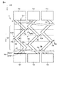
図6は、第2実施形態に係る表示装置DSPの配線部3を示す図である。図6は、隣り合う配線31、32、及び33を示している。
FIG. 6 is a view showing the
配線32及び33は、図5に示す配線31と同様の構造を有している。すなわち、配線32は、部分配線321と部分配線322とを有している。部分配線321は、方向Xに突出した屈曲部321aと、方向Xと逆方向に突出した屈曲部321bとを有している。部分配線322は、方向Xに突出した屈曲部322aと、方向Xと逆方向に突出した屈曲部322bとを有している。なお、図示した例では、部分配線321の配置は、図4に示す配線32の配置に相当する。
The
同様に、配線33は、部分配線331と部分配線332とを有している。部分配線331は、方向Xに突出した屈曲部331aと、方向Xと逆方向に突出した屈曲部331bとを有している。部分配線332は、方向Xに突出した屈曲部332aと、方向Xと逆方向に突出した屈曲部332bとを有している。なお、図示した例では、部分配線331の配置は、図4に示す配線33の配置に相当する。
Similarly, the
方向Yにおいて、屈曲部311aの位置は、配線32のいずれの屈曲部の位置とも一致していない。図示した例では、屈曲部311aの位置は、配線32において部分配線321と部分配線322とが接続される接続部の位置と一致している。一方、屈曲部311aの位置は、配線33の屈曲部332aの位置と一致している。
In the direction Y, the position of the bending
また、方向Yにおいて、屈曲部312aの位置は、配線32の屈曲部321aの位置と一致している。一方、屈曲部312aの位置は、配線33のいずれの屈曲部の位置とも一致していない。図示した例では、屈曲部312aの位置は、配線33において部分配線331と部分配線332とが接続される接続部の位置と一致している。
Further, in the direction Y, the position of the bending
本実施形態によれば、配線31は、屈曲部311aを有する部分配線311と、屈曲部312bを有する部分配線312とを含んでいる。屈曲部311aと屈曲部312bとは、互いに対向して配置され、且つ、方向Yにおける位置が異なっている。これにより、副基板101が折り曲げられたことによって生じる応力を分散させることができる。したがって、副基板101の全体として応力が所定の領域に集中することを抑制することができ、曲面領域CAにおける曲率を均一にすることがでる。この結果、配線31の断線を抑制することができ、信頼性を向上することが可能な表示装置を提供することができる。
According to the present embodiment, the
さらに、本実施形態によれば、部分配線311と部分配線312とは、複数個所に設けられた接続部CNにおいて接続されている。このため、部分配線311及び312の一方が破断した場合であっても、接続部CNを介して電流経路を確保することができる。したがって、表示装置DSPの動作が安定し、信頼性を向上することができる。
Furthermore, according to the present embodiment, the
[第3実施形態]
図7は、第3実施形態に係る表示装置DSPの配線31を示す図である。第3実施形態は、配線31が部分配線311及び312に加え、部分配線313を有している点で、第2実施形態と相違している。
Third Embodiment
FIG. 7 is a view showing the
部分配線(第3部分配線)313は、部分配線311及び312と同様の構造を有している。すなわち、部分配線313は、方向Xに突出した屈曲部(第3屈曲部)313aと、方向Xと逆方向に突出した屈曲部313bとを有している。屈曲部313aと313bとは、方向Yに(曲面領域CAにおいては周方向Cに)交互に並んでいる。また、部分配線313は、部分配線311と接続部CN31において接続され、部分配線312と接続部CN32において接続されている。これにより、部分配線313は、部分配線311及び312と同電位である。このような配線31には、一例として、電源電位が供給される。部分配線313は、部分配線311及び部分配線312の少なくとも一方と別層に形成され、接続部CN31または接続部CN32を介して互いに接続してもよいが、いずれも同層で形成されるようにしてもよい。
The partial wiring (third partial wiring) 313 has the same structure as the
方向Yにおいて、屈曲部313aの位置(第5位置)及び屈曲部313bの位置は、部分配線311の屈曲部311a及び311bの位置、及び部分配線312の屈曲部312a及び312bの位置のいずれとも一致していない。ここで、屈曲部313aの位置は、屈曲部313aが有する頂点P13aの位置に相当し、屈曲部313bの位置は、屈曲部313bが有する頂点P13bの位置に相当する。頂点P13aは、方向Yにおいて、屈曲部311bの頂点P11bと屈曲部312bの頂点P12bとの間に位置している。また、頂点P13bは、方向Yにおいて、屈曲部311aの頂点P11aと屈曲部312aの頂点P12aとの間に位置している。なお、このような構造の部分配線311、312、及び313は、方向Yに沿って、それぞれ位相を120度ずつずらして配置されているとみなすことができる。
In the direction Y, the position of the bending
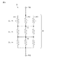
図8は、図7に示す配線31の等価回路を示す図である。部分配線311、312、及び313が束ねられた状態において、配線31は、全体として抵抗Rを有している。図8は、この配線31が方向Yに沿って分割された様子を示している。分割点Dは、上述の接続部CN31、CN32などに相当する。
FIG. 8 is a diagram showing an equivalent circuit of the
ここで、配線31を方向Yに沿って例えばn分割された場合の、分割された各セグメントSにおける部分配線311、312、及び313の抵抗がそれぞれrであるとする。あるセグメントSにおいて、部分配線311、312、及び313のうち、例えばいずれか1つが破断した場合、このセグメントSの抵抗は、r/2となる。したがって、破断が生じた後の全体の抵抗R’は、
R’=r/3・(n−1)+r/2
=r/3・n+r/6
=R(1+1/(2n))
となる。
Here, it is assumed that the resistances of the
R '= r / 3 · (n-1) + r / 2
= R / 3 · n + r / 6
= R (1 + 1 / (2 n))
It becomes.
第3実施形態においても、第2実施形態と同様の効果を得ることができる。さらに、本実施形態によれば、以下に説明するように、配線31が部分的に破断した場合であっても、配線31の全体の抵抗の変化を抑制することができる。
Also in the third embodiment, the same effect as that of the second embodiment can be obtained. Furthermore, according to the present embodiment, as described below, even when the
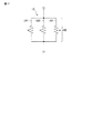
図11は、図10に示す比較例としての配線LEの等価回路を示している。配線LEが含む部分配線LE1、LE2、及びLE3の各抵抗をreとすると、配線LE全体の抵抗REは、re/3である。ここで、部分配線LE1、LE2、及びLE3のうち、例えばいずれか1つが破断した場合、配線LE全体の抵抗は、re/2となり、破断前の1.5倍に上昇する。 FIG. 11 shows an equivalent circuit of the wiring LE as the comparative example shown in FIG. Assuming that the resistances of the partial wirings LE1, LE2, and LE3 included in the wiring LE are re, the resistance RE of the entire wiring LE is re / 3. Here, for example, when any one of the partial wirings LE1, LE2, and LE3 is broken, the resistance of the entire wiring LE is re / 2, which is 1.5 times as high as that before the breakage.
一方、本実施形態によれば、図8を参照して説明したように、方向Y、すなわち配線31の延伸方向に沿って配線31を複数のセグメントSに分割しているため、分割された抵抗rを単位として、全体の抵抗REが変化する。したがって、部分配線311、312、及び313のうち、例えばいずれか1つが破断した場合であっても、図10及び図11に示す例と比較して、配線31の抵抗の上昇を抑制することができる。特に、分割数を十分に大きくすることで、配線31の全体の抵抗値の上昇を大幅に抑制することができる。したがって、配線31によって供給される信号の劣化を抑制することができ、表示装置DSPの信頼性を向上することができる。
On the other hand, according to the present embodiment, as described with reference to FIG. 8, since the
ここで、セグメントSの分割数を大きくするとは、例えば、配線に含まれる接続部の数を多くすることであり、言い換えると、接続部間の距離を短くすることである。また、第2実施形態、及び、第3実施形態において、1つの配線を構成する部分配線の数を2つまたは3つとしたがこれに限られない。1つの配線に4つ以上の部分配線が含まれてもよい。さらに、1つの接続部CNが接続する部分配線の数も2つに限らず、3つ以上の部分配線が同一の接続部CNで接続されるようにしてもよい。 Here, increasing the number of divisions of the segment S means, for example, increasing the number of connection portions included in the wiring, in other words, shortening the distance between the connection portions. Further, in the second embodiment and the third embodiment, although the number of partial wirings constituting one wiring is two or three, the present invention is not limited to this. One wire may include four or more partial wires. Furthermore, the number of partial wires connected by one connection portion CN is not limited to two, and three or more partial wires may be connected by the same connection portion CN.
[第4実施形態]
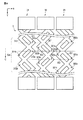
図9は、第4実施形態に係る表示装置DSPの配線31を示す図である。第4実施形態は、屈曲部が曲線状に形成されている点で、第3実施形態と相違している。図示した例では、屈曲部311a及び311bの曲率、屈曲部312a及び312bの曲率、及び屈曲部313a及び313bの曲率は、それぞれ等しい。なお、屈曲部の曲率は、屈曲部毎に異なっていてもよい。
Fourth Embodiment
FIG. 9 is a view showing the
第4実施形態においても、第3実施形態と同様の効果を得ることができる。さらに、本実施形態によれば、屈曲部を曲線状にすることによって、屈曲部内の所定の位置に応力が集中することを抑制することができる。すなわち、屈曲部内において応力をさらに均一化することができる。この結果、配線31の断線を抑制することができ、信頼性を向上することが可能な表示装置を提供することができる。
Also in the fourth embodiment, the same effect as that of the third embodiment can be obtained. Furthermore, according to the present embodiment, by forming the bent portion in a curved shape, it is possible to suppress concentration of stress at a predetermined position in the bent portion. That is, the stress can be further equalized in the bending portion. As a result, disconnection of the
以上の説明において、第1実施形態における配線31は、第2配線に相当し、第1実施形態における配線32は、第3配線に相当する。また、第2乃至第4実施形態における配線31は、第1配線に相当する。以下では、第1乃至第4実施形態に共通の構成について説明する。
In the above description, the
図12は、図1に示す表示装置DSPの平面領域PA1を示す断面図である。副基板101は、絶縁基板10、第1乃至第5絶縁膜11乃至15、スイッチング素子SW(SW1、SW2、SW3)、反射層RL、有機EL素子OLED(OLED1、OLED2、OLED3)、封止層16、などを備えている。
FIG. 12 is a cross-sectional view showing a flat area PA1 of the display device DSP shown in FIG. The sub-substrate 101 includes an insulating
絶縁基板10は、例えばポリイミド等の有機絶縁材料によって形成されている。図示した例では、支持部材71は、絶縁基板10の下に貼り付けられている。第1絶縁膜11は、絶縁基板10の上に形成されている。第1絶縁膜11は、絶縁基板10から有機EL素子OLEDへ向かう水分等の侵入を抑制するためのバリア層を含んでいてもよい。なお、支持部材71及び第1絶縁膜11の少なくとも一方は、省略されてもよい。
The insulating
スイッチング素子SWは、第1絶縁膜11の上に形成されている。スイッチング素子SWは、例えば薄膜トランジスタ(TFT;thin-film-transistor)により構成されている。図示した例では、スイッチング素子SWはトップゲート型であるが、ボトムゲート型であってもよい。以下では、スイッチング素子SW1を例として、その構成を説明する。
The switching element SW is formed on the first insulating
スイッチング素子SW1は、半導体層SC、ゲート電極GE、ソース電極SE、及び、ドレイン電極DEを備えている。 The switching element SW1 includes a semiconductor layer SC, a gate electrode GE, a source electrode SE, and a drain electrode DE.
半導体層SCは、第1絶縁膜11の上に形成され、第2絶縁膜12により覆われている。ゲート電極GEは、第2絶縁膜12の上に形成され、第3絶縁膜13により覆われている。ソース電極SE及びドレイン電極DEは、それぞれ第3絶縁膜13の上に形成されている。ソース電極SE及びドレイン電極DEは、第3絶縁膜13を半導体層SCまで貫通するコンタクトホールにおいて、半導体層SCにそれぞれ接触している。
The semiconductor layer SC is formed on the first insulating
ゲート電極GE、ソース電極SE及びドレイン電極DEを形成する材料は、例えば、アルミニウム(Al)、チタン(Ti)、銀(Ag)、モリブデン(Mo)、タングステン(W)、銅(Cu)、クロム(Cr)などの金属材料や、これらの金属材料を組み合わせた合金である。また、各電極は、単層構造であってもよいし、多層構造であってもよい。なお、各電極は、電極毎に異なる材料又は異なる層構造を有してもよい。第1乃至第3絶縁膜11乃至13は、酸化シリコン、窒化シリコン、酸窒化シリコン等の無機絶縁材料により形成されている。スイッチング素子SW1は、第4絶縁膜14により覆われている。第4絶縁膜は、有機絶縁材料により形成されている。
The material for forming the gate electrode GE, the source electrode SE, and the drain electrode DE is, for example, aluminum (Al), titanium (Ti), silver (Ag), molybdenum (Mo), tungsten (W), copper (Cu), chromium It is a metal material such as (Cr) or an alloy combining these metal materials. Each electrode may have a single-layer structure or a multi-layer structure. Each electrode may have different materials or different layer structures for each electrode. The first to third insulating
有機EL素子OLEDは、第4絶縁膜14の上に形成されている。図示した例では、有機EL素子OLEDは、絶縁基板10とは反対側に光を出射する所謂トップエミッションタイプであるが、この例に限らず、絶縁基板10の側に光を出射する所謂ボトムエミッションタイプであってもよい。一例では、有機EL素子OLED1は、赤色に発光する有機発光層ORG1を備え、有機EL素子OLED2は、青色に発光する有機発光層ORG2を備え、有機EL素子OLED3は、緑色に発光する有機発光層ORG3を備えている。以下では、有機EL素子OLED1を例として、その構成を説明する。
The organic EL element OLED is formed on the fourth insulating
有機EL素子OLED1は、画素電極PE1、共通電極CE、及び有機発光層ORG1により構成されている。 The organic EL element OLED1 is composed of a pixel electrode PE1, a common electrode CE, and an organic light emitting layer ORG1.
画素電極PE1は、第4絶縁膜14の上に設けられている。画素電極PE1は、有機EL素子OLED1の例えば陽極として機能する。画素電極PE1には、アノード電源配線を介して、電源電位(アノード電源電位PVDD)が供給される。画素電極PE1は、第4絶縁膜14内に設けられたコンタクトホールにおいて、スイッチング素子SW1のドレイン電極DEと接触し、スイッチング素子SW1と電気的に接続されている。有機発光層ORG1は、画素電極PE1の上に形成されている。有機発光層ORG1は、発光効率を向上するために、電子注入層、正孔注入層、電子輸送層、正孔輸送層等をさらに含んでいてもよい。共通電極CEは、有機発光層ORG1の上に形成されている。共通電極CEは、有機EL素子OLED1の例えば陰極として機能する。共通電極CEには、カソード電源配線を介して、電源電位(カソード電源電位PVSS)が供給される。共通電極CEと画素電極PE1とは、例えばインジウム・ティン・オキサイド(ITO)やインジウム・ジンク・オキサイド(IZO)等の透明な導電材料によって形成されている。以上のように構成された有機EL素子OLED1は、画素電極PE1と共通電極CEとの間に印加される電圧(あるいは電流)に応じた輝度で発光する。
The pixel electrode PE1 is provided on the fourth insulating
なお、トップエミッションタイプの場合には、有機EL素子OLED1は、図12に示すように、第4絶縁膜14と画素電極PE1との間に反射層RLを含んでいることが望ましい。反射層RLは、例えばアルミニウム、銀等の反射率の高い金属材料により形成されている。なお、反射層RLの反射面、すなわち有機発光層ORG1側の面は、図示したように平坦であってもよいし、光散乱性を付与するために凹凸が形成されていてもよい。
In the case of the top emission type, as shown in FIG. 12, it is desirable that the organic EL element OLED1 include the reflective layer RL between the fourth insulating
各有機EL素子OLEDは、有機絶縁材料からなる第5絶縁膜(リブ)15により、画素PXごとに区画されている。すなわち、有機発光層ORG1、ORG2、及びORG3は、第5絶縁膜15と第5絶縁膜15との間に位置している。図示した例では、共通電極CEは、有機発光層ORG1、ORG2、及びORG3と接するとともに、第5絶縁膜15とも接している。
Each organic EL element OLED is partitioned for each pixel PX by a fifth insulating film (rib) 15 made of an organic insulating material. That is, the organic light emitting layers ORG1, ORG2, and ORG3 are located between the fifth insulating
なお、表示装置DSPは、複数の画素PXに亘って共通の有機発光層を有していてもよい。このような構成においては、表示装置DSPは、有機EL素子OLEDと対向する位置にカラーフィルタを備えている。カラーフィルタは、例えば赤色、緑色、青色等に着色された樹脂材料によって形成される。 The display device DSP may have a common organic light emitting layer across a plurality of pixels PX. In such a configuration, the display device DSP includes a color filter at a position facing the organic EL element OLED. The color filter is formed of, for example, a resin material colored in red, green, blue or the like.
封止層16は、有機EL素子OLEDを覆っている。封止層16は、有機EL素子OLEDへの水分や酸素の侵入を抑制し、有機EL素子OLEDの劣化を抑制する。封止層16は、第1無機膜161、有機膜162、及び第2無機膜163を備えている。
The
第1無機膜161は、有機EL素子OLEDの上に形成されている。図示した例では、第1無機膜161は、共通電極CEと接している。第2無機膜163は、第1無機膜161の上に位置している。有機膜162は、第1無機膜161と第2無機膜163の間に位置し、第1無機膜161及び第2無機膜163と接している。
The first
第1無機膜161及び第2無機膜163は、有機EL素子OLED側への水分の侵入を遮断する機能を有している。第1無機膜161及び第2無機膜163は、透明であり、例えば窒化シリコンによって形成されている。有機膜162は、透明な有機材料によって形成されている。なお、ここでの透明とは、透過光が表示に影響のない範囲で着色されることを許容するものである。
The first
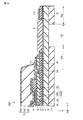
図13は、平面領域PA1、曲面領域CA、及び平面領域PA2を示す断面図である。ここでは、模式的に、曲面領域CAが折り曲げられる前の状態を示している。平面領域PA1、曲面領域CA、及び平面領域PA2は、この順で、方向Yに沿って並んでいる。 FIG. 13 is a cross-sectional view showing the plane area PA1, the curved area CA, and the plane area PA2. Here, a state before the curved surface area CA is bent is schematically shown. The plane area PA1, the curved area CA, and the plane area PA2 are arranged in this order along the direction Y.
表示装置DSPは、支持部材71、絶縁基板10、第1乃至第5絶縁膜11乃至15、反射層RL、有機EL素子OLED、及び封止層16、に加え、支持部材72、端子T11及びT12、配線31、及び保護膜8を備えている。
The display device DSP includes a
絶縁基板10は、平面領域PA1、曲面領域CA、及び平面領域PA2に亘って位置している。支持部材71は、平面領域PA1において、絶縁基板10の下面に貼り付けられている。支持部材72は、平面領域PA2において、絶縁基板10の下面に貼り付けられている。曲面領域CAは、支持部材71及び72が設けられていない領域に相当する。
The insulating
平面領域PA2において、第1乃至第3絶縁膜11乃至13は、この順で積層されている。一方、曲面領域CAにおいて、第1乃至第3絶縁膜11乃至13は、設けられていない。
In the planar area PA2, the first to third insulating
配線31は、平面領域PA1、曲面領域CA、及び平面領域PA2に亘って形成されている。平面領域PA1において、配線31は、第3絶縁膜13と第4絶縁膜14との間に位置している。図示した例では、配線31は、平面領域PA1において、第2絶縁膜12及び第1絶縁膜11とも接している。曲面領域CAにおいて、配線31は、絶縁基板10の上に形成されている。平面領域PA2において、配線31は、第3絶縁膜13の上に形成されている。図示した例では、配線31は、平面領域PA2において、第2絶縁膜12及び第1絶縁膜11とも接している。
The
端子T11は、平面領域PA1において、第4絶縁膜14の上に形成されている。端子T11は、第4絶縁膜14を貫通するコンタクトホールCHにおいて、配線31と接している。共通電極CEは、有機EL素子OLEDよりも曲面領域CA側に延在し、端子T11と接している。これにより、有機EL素子OLEDと配線31とが電気的に接続される。端子T12は、平面領域PA2において、配線31の上に形成されている。
The terminal T11 is formed on the fourth insulating
上述したように、曲面領域CAにおいて、無機絶縁材料からなる第1乃至第3絶縁膜11乃至13が除去されているため、配線31は、絶縁基板10と接している。このように有機絶縁膜よりも剛性の高い無機絶縁膜を除去することにより、曲面領域CAを折り曲げた際に、無機絶縁膜におけるクラックの発生を防ぐことができる。このため、配線31の破断を抑制することができる。
As described above, since the first to third insulating
さらに、曲面領域CAにおいて、配線31は、有機絶縁材料からなる保護膜8によって覆われている。保護膜8は、有機材料に対して紫外線照射によって硬化することで形成される。このような保護膜8が設けられることにより、曲面領域CAが折り曲げられた際に、方向Zにおいて、折り曲げによる応力の中立面の位置を配線31の近傍に設定することができる。このため、曲面領域CAにおける配線31への負荷を軽減することができる。
Furthermore, in the curved surface area CA, the
なお、本発明のいくつかの実施形態を説明したが、これらの実施形態は、例として提示したものであり、発明の範囲を限定することは意図していない。これらの新規な実施形態は、その他の様々な形態で実施されることが可能であり、発明の要旨を逸脱しない範囲で、種々の省略、置き換え、変更を行うことができる。これらの実施形態やその変形は、発明の範囲や要旨に含まれるとともに、特許請求の範囲に記載された発明とその均等の範囲に含まれる。 While certain embodiments of the present invention have been described, these embodiments have been presented by way of example only, and are not intended to limit the scope of the invention. These novel embodiments can be implemented in various other forms, and various omissions, substitutions, and modifications can be made without departing from the scope of the invention. These embodiments and modifications thereof are included in the scope and the gist of the invention, and are included in the invention described in the claims and the equivalents thereof.
1…基板、2…ドライバ、3…配線部、4…カバー部材、5…偏光板、6…接着剤、71,72…支持部材、8…保護膜、10…絶縁基板、31,32,33…配線、311,312,313…部分配線、31a,32a,311a,312b…屈曲部、P1a,P2a,P11a,P12b…頂点、OLED…有機EL素子、CA…曲面領域、PA1,PA2…平面領域。
DESCRIPTION OF
Claims (16)
前記基板に設けられた表示素子と、
前記基板に設けられ、前記表示素子を駆動する駆動部と、
前記表示素子と電気的に接続された第1配線と、
を備え、
前記第1配線は、第1方向に突出した第1屈曲部と、前記第1方向の逆方向に突出した第2屈曲部とを有し、
前記第1方向、及び前記第1方向と交差する第2方向において、前記第1屈曲部の第1位置と前記第2屈曲部の第2位置とは、異なっている、表示装置。 A substrate,
A display element provided on the substrate;
A driving unit provided on the substrate and driving the display element;
A first wire electrically connected to the display element;
Equipped with
The first wiring includes a first bent portion protruding in a first direction and a second bent portion protruding in a direction opposite to the first direction,
The display device in which the first position of the first bending portion and the second position of the second bending portion are different in the first direction and a second direction intersecting the first direction.
前記第2屈曲部は、前記第2位置に第2頂点を有している、請求項1に記載の表示装置。 The first bending portion has a first vertex at the first position,
The display device according to claim 1, wherein the second bending portion has a second vertex at the second position.
前記第1部分配線の前記第1屈曲部と、前記第2部分配線の前記第2屈曲部とは、前記第1接続部と前記第2接続部との間に位置し、互いに離間している、請求項3に記載の表示装置。 The connection unit includes a first connection unit and a second connection unit,
The first bent portion of the first partial wiring and the second bent portion of the second partial wiring are located between the first connection portion and the second connection portion and are separated from each other. The display device according to claim 3.
前記第2方向において、前記第3屈曲部の第5位置は、前記第1位置及び前記第2位置と異なっている、請求項1乃至7のいずれか1項に記載の表示装置。 The first wire further includes a third partial wire including a third bent portion,
The display device according to any one of claims 1 to 7, wherein a fifth position of the third bending portion is different from the first position and the second position in the second direction.
前記第1副基板は、曲面領域を有し、
前記表示素子及び前記駆動部は、前記第1副基板に設けられている、請求項1乃至9のいずれか1項に記載の表示装置。 The substrate includes a first sub-substrate and a second sub-substrate connected to the first sub-substrate,
The first sub-substrate has a curved surface area,
The display device according to any one of claims 1 to 9, wherein the display element and the drive unit are provided on the first sub-substrate.
前記第2副基板は、曲面領域を有し、
前記表示素子は、前記第1副基板に設けられ、
前記駆動部は、前記第2副基板に設けられている、請求項1乃至9のいずれか1項に記載の表示装置。 The substrate includes a first sub-substrate and a second sub-substrate connected to the first sub-substrate,
The second sub-substrate has a curved surface area,
The display element is provided on the first sub-substrate,
The display device according to claim 1, wherein the drive unit is provided on the second sub-substrate.
前記基板に設けられた表示素子と、
前記基板に設けられ、前記表示素子を駆動する駆動部と、
前記表示素子と前記駆動部とを電気的に接続する第2配線及び第3配線と、
を備え、
前記第2配線と前記第3配線とは、第1方向に沿って隣り合い、
前記第2配線は、第4屈曲部を有し、
前記第3配線は、第5屈曲部を有し、
前記第1方向と交差する第2方向において、前記第4屈曲部の第6位置と前記第5屈曲部の第7位置とは、異なっている、表示装置。 A substrate,
A display element provided on the substrate;
A driving unit provided on the substrate and driving the display element;
A second wiring and a third wiring that electrically connect the display element and the drive unit;
Equipped with
The second wiring and the third wiring are adjacent to each other along a first direction,
The second wiring has a fourth bent portion,
The third wiring has a fifth bent portion,
The display device in which the sixth position of the fourth bent portion is different from the seventh position of the fifth bent portion in a second direction intersecting the first direction.
前記第5屈曲部は、前記第7位置に第4頂点を有している、請求項12に記載の表示装置。 The fourth bending portion has a third vertex at the sixth position,
The display device according to claim 12, wherein the fifth bending portion has a fourth vertex at the seventh position.
前記第1副基板は、曲面領域を有し、
前記表示素子及び前記駆動部は、前記第1副基板に設けられている、請求項12又は13に記載の表示装置。 The substrate includes a first sub-substrate and a second sub-substrate connected to the first sub-substrate,
The first sub-substrate has a curved surface area,
The display device according to claim 12, wherein the display element and the drive unit are provided on the first sub-substrate.
前記第2副基板は、曲面領域を有し、
前記表示素子は、前記第1副基板に設けられ、
前記駆動部は、前記第2副基板に設けられている、請求項12又は13に記載の表示装置。 The substrate includes a first sub-substrate and a second sub-substrate connected to the first sub-substrate,
The second sub-substrate has a curved surface area,
The display element is provided on the first sub-substrate,
The display device according to claim 12, wherein the driving unit is provided on the second sub substrate.
Priority Applications (2)
| Application Number | Priority Date | Filing Date | Title |
|---|---|---|---|
| JP2018004505A JP2019124792A (en) | 2018-01-15 | 2018-01-15 | Display device |
| US16/237,037 US10756158B2 (en) | 2018-01-15 | 2018-12-31 | Display device |
Applications Claiming Priority (1)
| Application Number | Priority Date | Filing Date | Title |
|---|---|---|---|
| JP2018004505A JP2019124792A (en) | 2018-01-15 | 2018-01-15 | Display device |
Publications (1)
| Publication Number | Publication Date |
|---|---|
| JP2019124792A true JP2019124792A (en) | 2019-07-25 |
Family
ID=67214307
Family Applications (1)
| Application Number | Title | Priority Date | Filing Date |
|---|---|---|---|
| JP2018004505A Pending JP2019124792A (en) | 2018-01-15 | 2018-01-15 | Display device |
Country Status (2)
| Country | Link |
|---|---|
| US (1) | US10756158B2 (en) |
| JP (1) | JP2019124792A (en) |
Families Citing this family (2)
| Publication number | Priority date | Publication date | Assignee | Title |
|---|---|---|---|---|
| CN110164950B (en) * | 2019-06-27 | 2021-09-10 | 上海天马微电子有限公司 | Stretchable flexible display panel and display device |
| CN111833745A (en) | 2020-07-03 | 2020-10-27 | 武汉华星光电半导体显示技术有限公司 | Array substrates and display panels |
Citations (3)
| Publication number | Priority date | Publication date | Assignee | Title |
|---|---|---|---|---|
| JP2004119871A (en) * | 2002-09-27 | 2004-04-15 | Denso Corp | Multilayer printed circuit board |
| US20160174304A1 (en) * | 2014-12-10 | 2016-06-16 | Lg Display Co., Ltd. | Flexible display device with multiple types of micro-coating layers |
| JP2017533583A (en) * | 2014-10-10 | 2017-11-09 | アップル インコーポレイテッド | Signal trace pattern of flexible board |
Family Cites Families (8)
| Publication number | Priority date | Publication date | Assignee | Title |
|---|---|---|---|---|
| CA2829388C (en) * | 2011-03-09 | 2018-09-25 | Flex Lighting Ii, Llc | Light emitting device with adjustable light output profile |
| KR101971201B1 (en) * | 2012-08-20 | 2019-04-23 | 삼성디스플레이 주식회사 | Dual display device and method for manufacturing thereof |
| US9740035B2 (en) * | 2013-02-15 | 2017-08-22 | Lg Display Co., Ltd. | Flexible organic light emitting display device and method for manufacturing the same |
| KR102085961B1 (en) * | 2013-12-24 | 2020-03-06 | 엘지디스플레이 주식회사 | Flexible organic light emitting display and method of manufacturing the same |
| US9349758B2 (en) * | 2014-09-30 | 2016-05-24 | Lg Display Co., Ltd. | Flexible display device with divided power lines and manufacturing method for the same |
| KR102611499B1 (en) | 2015-12-15 | 2023-12-06 | 엘지디스플레이 주식회사 | Flexible display device |
| CN107809873B (en) * | 2016-09-09 | 2021-09-14 | 三星显示有限公司 | Display device and method of manufacturing electronic device using the same |
| KR102636680B1 (en) * | 2016-09-30 | 2024-02-14 | 엘지디스플레이 주식회사 | Backplane Substrate and Flexible Display Using the Same |
-
2018
- 2018-01-15 JP JP2018004505A patent/JP2019124792A/en active Pending
- 2018-12-31 US US16/237,037 patent/US10756158B2/en active Active
Patent Citations (3)
| Publication number | Priority date | Publication date | Assignee | Title |
|---|---|---|---|---|
| JP2004119871A (en) * | 2002-09-27 | 2004-04-15 | Denso Corp | Multilayer printed circuit board |
| JP2017533583A (en) * | 2014-10-10 | 2017-11-09 | アップル インコーポレイテッド | Signal trace pattern of flexible board |
| US20160174304A1 (en) * | 2014-12-10 | 2016-06-16 | Lg Display Co., Ltd. | Flexible display device with multiple types of micro-coating layers |
Also Published As
| Publication number | Publication date |
|---|---|
| US10756158B2 (en) | 2020-08-25 |
| US20190221632A1 (en) | 2019-07-18 |
Similar Documents
| Publication | Publication Date | Title |
|---|---|---|
| US11825713B2 (en) | Display device | |
| US10014361B2 (en) | Organic light emitting display device | |
| KR20250158010A (en) | Display panel | |
| US10903297B2 (en) | Bidirectional organic light emitting display device | |
| US9871089B2 (en) | Display device | |
| US11417722B2 (en) | Display device including a low resistance cathode wiring | |
| US10608199B2 (en) | Display apparatus | |
| JP6762845B2 (en) | Display device and wiring board | |
| CN113903774B (en) | Transparent display device | |
| JP7098425B2 (en) | Display device | |
| JP7077001B2 (en) | Display device | |
| US10561022B2 (en) | Display device | |
| US10573709B2 (en) | Display device | |
| US10756158B2 (en) | Display device | |
| KR20190043828A (en) | Organic light emitting display device | |
| CN114613825B (en) | Display panel and display device | |
| CN114628460B (en) | Display device | |
| WO2021009811A1 (en) | Display device | |
| US12171121B2 (en) | Transparent display device capable of minimizing size of non-transmissive area | |
| CN224083988U (en) | Display device | |
| US20260068495A1 (en) | Display device | |
| JP2018156850A (en) | Display device | |
| JP2025126567A (en) | display device |
Legal Events
| Date | Code | Title | Description |
|---|---|---|---|
| A621 | Written request for application examination |
Free format text: JAPANESE INTERMEDIATE CODE: A621 Effective date: 20200707 |
|
| A977 | Report on retrieval |
Free format text: JAPANESE INTERMEDIATE CODE: A971007 Effective date: 20210629 |
|
| A131 | Notification of reasons for refusal |
Free format text: JAPANESE INTERMEDIATE CODE: A131 Effective date: 20210824 |
|
| A02 | Decision of refusal |
Free format text: JAPANESE INTERMEDIATE CODE: A02 Effective date: 20220301 |