JP2019140160A - 発光部品実装装置および発光部品実装方法 - Google Patents
発光部品実装装置および発光部品実装方法 Download PDFInfo
- Publication number
- JP2019140160A JP2019140160A JP2018019714A JP2018019714A JP2019140160A JP 2019140160 A JP2019140160 A JP 2019140160A JP 2018019714 A JP2018019714 A JP 2018019714A JP 2018019714 A JP2018019714 A JP 2018019714A JP 2019140160 A JP2019140160 A JP 2019140160A
- Authority
- JP
- Japan
- Prior art keywords
- light emitting
- emitting component
- light
- unit
- luminance distribution
- Prior art date
- Legal status (The legal status is an assumption and is not a legal conclusion. Google has not performed a legal analysis and makes no representation as to the accuracy of the status listed.)
- Granted
Links
Images




Classifications
-
- H—ELECTRICITY
- H05—ELECTRIC TECHNIQUES NOT OTHERWISE PROVIDED FOR
- H05K—PRINTED CIRCUITS; CASINGS OR CONSTRUCTIONAL DETAILS OF ELECTRIC APPARATUS; MANUFACTURE OF ASSEMBLAGES OF ELECTRICAL COMPONENTS
- H05K13/00—Apparatus or processes specially adapted for manufacturing or adjusting assemblages of electric components
- H05K13/04—Mounting of components, e.g. of leadless components
- H05K13/0404—Pick-and-place heads or apparatus, e.g. with jaws
- H05K13/0408—Incorporating a pick-up tool
-
- F—MECHANICAL ENGINEERING; LIGHTING; HEATING; WEAPONS; BLASTING
- F21—LIGHTING
- F21V—FUNCTIONAL FEATURES OR DETAILS OF LIGHTING DEVICES OR SYSTEMS THEREOF; STRUCTURAL COMBINATIONS OF LIGHTING DEVICES WITH OTHER ARTICLES, NOT OTHERWISE PROVIDED FOR
- F21V19/00—Fastening of light sources or lamp holders
- F21V19/001—Fastening of light sources or lamp holders the light sources being semiconductors devices, e.g. LEDs
- F21V19/0015—Fastening arrangements intended to retain light sources
- F21V19/0025—Fastening arrangements intended to retain light sources the fastening means engaging the conductors of the light source, i.e. providing simultaneous fastening of the light sources and their electric connections
-
- H—ELECTRICITY
- H05—ELECTRIC TECHNIQUES NOT OTHERWISE PROVIDED FOR
- H05K—PRINTED CIRCUITS; CASINGS OR CONSTRUCTIONAL DETAILS OF ELECTRIC APPARATUS; MANUFACTURE OF ASSEMBLAGES OF ELECTRICAL COMPONENTS
- H05K13/00—Apparatus or processes specially adapted for manufacturing or adjusting assemblages of electric components
- H05K13/04—Mounting of components, e.g. of leadless components
- H05K13/0404—Pick-and-place heads or apparatus, e.g. with jaws
- H05K13/0413—Pick-and-place heads or apparatus, e.g. with jaws with orientation of the component while holding it; Drive mechanisms for gripping tools, e.g. lifting, lowering or turning of gripping tools
-
- F—MECHANICAL ENGINEERING; LIGHTING; HEATING; WEAPONS; BLASTING
- F21—LIGHTING
- F21V—FUNCTIONAL FEATURES OR DETAILS OF LIGHTING DEVICES OR SYSTEMS THEREOF; STRUCTURAL COMBINATIONS OF LIGHTING DEVICES WITH OTHER ARTICLES, NOT OTHERWISE PROVIDED FOR
- F21V14/00—Controlling the distribution of the light emitted by adjustment of elements
- F21V14/02—Controlling the distribution of the light emitted by adjustment of elements by movement of light sources
-
- G—PHYSICS
- G01—MEASURING; TESTING
- G01D—MEASURING NOT SPECIALLY ADAPTED FOR A SPECIFIC VARIABLE; ARRANGEMENTS FOR MEASURING TWO OR MORE VARIABLES NOT COVERED IN A SINGLE OTHER SUBCLASS; TARIFF METERING APPARATUS; MEASURING OR TESTING NOT OTHERWISE PROVIDED FOR
- G01D5/00—Mechanical means for transferring the output of a sensing member; Means for converting the output of a sensing member to another variable where the form or nature of the sensing member does not constrain the means for converting; Transducers not specially adapted for a specific variable
- G01D5/26—Mechanical means for transferring the output of a sensing member; Means for converting the output of a sensing member to another variable where the form or nature of the sensing member does not constrain the means for converting; Transducers not specially adapted for a specific variable characterised by optical transfer means, i.e. using infrared, visible, or ultraviolet light
-
- H—ELECTRICITY
- H05—ELECTRIC TECHNIQUES NOT OTHERWISE PROVIDED FOR
- H05K—PRINTED CIRCUITS; CASINGS OR CONSTRUCTIONAL DETAILS OF ELECTRIC APPARATUS; MANUFACTURE OF ASSEMBLAGES OF ELECTRICAL COMPONENTS
- H05K13/00—Apparatus or processes specially adapted for manufacturing or adjusting assemblages of electric components
- H05K13/0015—Orientation; Alignment; Positioning
-
- H—ELECTRICITY
- H05—ELECTRIC TECHNIQUES NOT OTHERWISE PROVIDED FOR
- H05K—PRINTED CIRCUITS; CASINGS OR CONSTRUCTIONAL DETAILS OF ELECTRIC APPARATUS; MANUFACTURE OF ASSEMBLAGES OF ELECTRICAL COMPONENTS
- H05K13/00—Apparatus or processes specially adapted for manufacturing or adjusting assemblages of electric components
- H05K13/08—Monitoring manufacture of assemblages
-
- H—ELECTRICITY
- H05—ELECTRIC TECHNIQUES NOT OTHERWISE PROVIDED FOR
- H05K—PRINTED CIRCUITS; CASINGS OR CONSTRUCTIONAL DETAILS OF ELECTRIC APPARATUS; MANUFACTURE OF ASSEMBLAGES OF ELECTRICAL COMPONENTS
- H05K13/00—Apparatus or processes specially adapted for manufacturing or adjusting assemblages of electric components
- H05K13/08—Monitoring manufacture of assemblages
- H05K13/081—Integration of optical monitoring devices in assembly lines; Processes using optical monitoring devices specially adapted for controlling devices or machines in assembly lines
- H05K13/0813—Controlling of single components prior to mounting, e.g. orientation, component geometry
-
- H—ELECTRICITY
- H10—SEMICONDUCTOR DEVICES; ELECTRIC SOLID-STATE DEVICES NOT OTHERWISE PROVIDED FOR
- H10H—INORGANIC LIGHT-EMITTING SEMICONDUCTOR DEVICES HAVING POTENTIAL BARRIERS
- H10H20/00—Individual inorganic light-emitting semiconductor devices having potential barriers, e.g. light-emitting diodes [LED]
- H10H20/01—Manufacture or treatment
-
- H—ELECTRICITY
- H10—SEMICONDUCTOR DEVICES; ELECTRIC SOLID-STATE DEVICES NOT OTHERWISE PROVIDED FOR
- H10H—INORGANIC LIGHT-EMITTING SEMICONDUCTOR DEVICES HAVING POTENTIAL BARRIERS
- H10H29/00—Integrated devices, or assemblies of multiple devices, comprising at least one light-emitting semiconductor element covered by group H10H20/00
- H10H29/10—Integrated devices comprising at least one light-emitting semiconductor component covered by group H10H20/00
- H10H29/14—Integrated devices comprising at least one light-emitting semiconductor component covered by group H10H20/00 comprising multiple light-emitting semiconductor components
- H10H29/142—Two-dimensional arrangements, e.g. asymmetric LED layout
-
- H—ELECTRICITY
- H10—SEMICONDUCTOR DEVICES; ELECTRIC SOLID-STATE DEVICES NOT OTHERWISE PROVIDED FOR
- H10W—GENERIC PACKAGES, INTERCONNECTIONS, CONNECTORS OR OTHER CONSTRUCTIONAL DETAILS OF DEVICES COVERED BY CLASS H10
- H10W90/00—Package configurations
-
- H—ELECTRICITY
- H10—SEMICONDUCTOR DEVICES; ELECTRIC SOLID-STATE DEVICES NOT OTHERWISE PROVIDED FOR
- H10H—INORGANIC LIGHT-EMITTING SEMICONDUCTOR DEVICES HAVING POTENTIAL BARRIERS
- H10H20/00—Individual inorganic light-emitting semiconductor devices having potential barriers, e.g. light-emitting diodes [LED]
- H10H20/80—Constructional details
Landscapes
- Engineering & Computer Science (AREA)
- Manufacturing & Machinery (AREA)
- Microelectronics & Electronic Packaging (AREA)
- Operations Research (AREA)
- General Engineering & Computer Science (AREA)
- Physics & Mathematics (AREA)
- General Physics & Mathematics (AREA)
- Supply And Installment Of Electrical Components (AREA)
- Length Measuring Devices By Optical Means (AREA)
Abstract
Description
3 基板
8 ヘッド移動機構
9 装着ヘッド
11 基板認識カメラ
12 部品認識カメラ
13 測定ステージ
17 通電端子
20 発光部品
21 発光部
Lc 輝度分布中心
OP 光軸基準点
Claims (7)
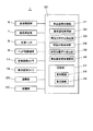
- 発光部が設けられた発光部品を装着ヘッドにより保持して基板に装着する発光部品実装装置であって、
前記発光部を発光させて発光部の輝度分布を測定し、この測定結果から前記発光部における輝度分布中心の位置を検出する輝度分布測定部と、
前記装着ヘッドを移動させるヘッド移動機構と、
前記検出された前記輝度分布中心の位置に基づいて前記ヘッド移動機構を制御する制御部と、を備える、発光部品実装装置。 - 前記輝度分布測定部は、
前記発光部品に通電を行う通電部と、
前記発光部品を上方から撮像する第1の撮像部と、
前記第1の撮像部による撮像結果を認識処理することにより前記輝度分布中心の位置を求める輝度分布中心検出部と、を備える、請求項1に記載の発光部品実装装置。 - 前記第1の撮像部による撮像結果を認識処理することにより前記発光部品の外形を検出する部品外形検出部と、をさらに備え、
前記制御部は、前記部品外形検出部の検出結果を加味して前記ヘッド移動機構を制御する、請求項2に記載の発光部品実装装置。 - 前記通電部は、
前記発光部品が載置される測定ステージと、
前記測定ステージの上面に形成され前記発光部品へ通電する通電端子とを備え、
前記第1の撮像部は、前記測定ステージに載置された前記発光部品を撮像することを特徴とする請求項2または3に記載の発光部品実装装置。 - 前記測定ステージは前記発光部品を吸着する吸着部を備えた、請求項4に記載の発光部品実装装置。
- 前記装着ヘッドに保持された前記発光部品を下方から撮像する第2の撮像部と、前記第2の撮像部による撮像結果を認識処理することにより前記発光部品の前記装着ヘッドにおける位置ずれを検出する部品位置ずれ検出部とをさらに備え、
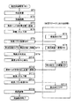
前記制御部は、前記部品位置ずれ検出部の検出結果を加味して前記ヘッド移動機構を制御する、請求項1から5のいずれかに記載の発光部品実装装置。 - 発光部が設けられた発光部品を装着ヘッドにより保持して基板に装着する発光部品実装方法であって、
前記発光部を発光させて発光部の輝度分布を測定し、この測定結果から前記発光部における輝度分布中心の位置を検出する輝度分布測定工程と、
前記発光部品を保持した装着ヘッドを移動させるヘッド移動工程と、
前記ヘッド移動工程において、前記検出された前記輝度分布中心の位置に基づいて前記装着ヘッドを移動させる、発光部品実装方法。
Priority Applications (4)
| Application Number | Priority Date | Filing Date | Title |
|---|---|---|---|
| JP2018019714A JP7178541B2 (ja) | 2018-02-07 | 2018-02-07 | 発光部品実装装置および発光部品実装方法 |
| US16/247,748 US11293626B2 (en) | 2018-02-07 | 2019-01-15 | Light emitting component mounting method |
| CN201910102817.2A CN110121255B (zh) | 2018-02-07 | 2019-01-31 | 发光部件安装装置以及发光部件安装方法 |
| DE102019201289.2A DE102019201289A1 (de) | 2018-02-07 | 2019-02-01 | Halter für ein lichtemittierendes Bauteil und Verfahren zur Befestigung eines lichtemittierenden Bauteils |
Applications Claiming Priority (1)
| Application Number | Priority Date | Filing Date | Title |
|---|---|---|---|
| JP2018019714A JP7178541B2 (ja) | 2018-02-07 | 2018-02-07 | 発光部品実装装置および発光部品実装方法 |
Publications (3)
| Publication Number | Publication Date |
|---|---|
| JP2019140160A true JP2019140160A (ja) | 2019-08-22 |
| JP2019140160A5 JP2019140160A5 (ja) | 2021-05-20 |
| JP7178541B2 JP7178541B2 (ja) | 2022-11-28 |
Family
ID=67309003
Family Applications (1)
| Application Number | Title | Priority Date | Filing Date |
|---|---|---|---|
| JP2018019714A Active JP7178541B2 (ja) | 2018-02-07 | 2018-02-07 | 発光部品実装装置および発光部品実装方法 |
Country Status (4)
| Country | Link |
|---|---|
| US (1) | US11293626B2 (ja) |
| JP (1) | JP7178541B2 (ja) |
| CN (1) | CN110121255B (ja) |
| DE (1) | DE102019201289A1 (ja) |
Cited By (1)
| Publication number | Priority date | Publication date | Assignee | Title |
|---|---|---|---|---|
| JP2021072305A (ja) * | 2019-10-29 | 2021-05-06 | パナソニックIpマネジメント株式会社 | 部品実装装置および実装基板の製造方法 |
Families Citing this family (1)
| Publication number | Priority date | Publication date | Assignee | Title |
|---|---|---|---|---|
| CN113242688B (zh) * | 2021-06-15 | 2022-09-20 | 重庆睿博光电股份有限公司 | 内饰小灯全自动装配线 |
Citations (6)
| Publication number | Priority date | Publication date | Assignee | Title |
|---|---|---|---|---|
| JPH0818164A (ja) * | 1994-06-27 | 1996-01-19 | Sony Corp | 発光デバイスの組立装置 |
| JP2000286452A (ja) * | 1999-03-29 | 2000-10-13 | Fuji Photo Film Co Ltd | 発光素子の発光中心検出方法 |
| JP2015159285A (ja) * | 2014-02-14 | 2015-09-03 | エーエスエム・アセンブリー・システムズ・ゲーエムベーハー・ウント・コ・カーゲー | 対向面に存在する構造的特徴を有する部品の光学的測定 |
| JP2015233121A (ja) * | 2014-06-09 | 2015-12-24 | 三星電子株式会社Samsung Electronics Co.,Ltd. | 光源モジュールの不良検査方法及び光源モジュールの製造方法 |
| JP2016100379A (ja) * | 2014-11-19 | 2016-05-30 | パナソニックIpマネジメント株式会社 | 部品搭載装置および部品搭載方法ならびに部品搭載システム |
| JP2017139388A (ja) * | 2016-02-04 | 2017-08-10 | 富士機械製造株式会社 | 実装装置 |
Family Cites Families (14)
| Publication number | Priority date | Publication date | Assignee | Title |
|---|---|---|---|---|
| JP2983804B2 (ja) * | 1993-08-02 | 1999-11-29 | シャープ株式会社 | 発光素子の発光点検出方法および位置決め装置 |
| JP2000150970A (ja) * | 1998-11-18 | 2000-05-30 | Fuji Photo Film Co Ltd | 発光素子のボンディング方法および装置 |
| US6208419B1 (en) | 1998-11-18 | 2001-03-27 | Fuji Photo Film Co., Ltd. | Method of and apparatus for bonding light-emitting element |
| WO2004016064A1 (en) * | 2002-08-08 | 2004-02-19 | Matsushita Electric Industrial Co., Ltd. | Device and method for detecting whether or not component holder is good, and apparatus and method for mounting electronic component |
| JP2005003385A (ja) * | 2003-06-09 | 2005-01-06 | Mitsutoyo Corp | 画像測定方法、および画像測定装置 |
| JP2007065414A (ja) * | 2005-08-31 | 2007-03-15 | Sharp Corp | バックライト製造方法 |
| US7967652B2 (en) * | 2009-02-19 | 2011-06-28 | Cree, Inc. | Methods for combining light emitting devices in a package and packages including combined light emitting devices |
| JP5338773B2 (ja) * | 2010-08-26 | 2013-11-13 | パナソニック株式会社 | 部品実装用装置および撮像用の照明装置ならびに照明方法 |
| JP2013152207A (ja) * | 2011-12-31 | 2013-08-08 | Shibaura Mechatronics Corp | 検査装置及び検査方法 |
| JP6259274B2 (ja) * | 2012-12-11 | 2018-01-10 | ヤマハ発動機株式会社 | 部品装着装置 |
| JP6450923B2 (ja) | 2013-12-20 | 2019-01-16 | パナソニックIpマネジメント株式会社 | 電子部品実装システムおよび電子部品実装方法ならびに電子部品実装装置 |
| CN106537615B (zh) * | 2014-08-04 | 2019-08-20 | 株式会社富士 | 安装装置 |
| JP6398082B2 (ja) * | 2015-02-26 | 2018-10-03 | パナソニックIpマネジメント株式会社 | 部品実装方法および部品実装装置 |
| KR102240592B1 (ko) * | 2016-12-07 | 2021-04-15 | 야마하하쓰도키 가부시키가이샤 | 표면 실장기, 부품 인식 장치, 부품 인식 방법 |
-
2018
- 2018-02-07 JP JP2018019714A patent/JP7178541B2/ja active Active
-
2019
- 2019-01-15 US US16/247,748 patent/US11293626B2/en active Active
- 2019-01-31 CN CN201910102817.2A patent/CN110121255B/zh active Active
- 2019-02-01 DE DE102019201289.2A patent/DE102019201289A1/de active Pending
Patent Citations (6)
| Publication number | Priority date | Publication date | Assignee | Title |
|---|---|---|---|---|
| JPH0818164A (ja) * | 1994-06-27 | 1996-01-19 | Sony Corp | 発光デバイスの組立装置 |
| JP2000286452A (ja) * | 1999-03-29 | 2000-10-13 | Fuji Photo Film Co Ltd | 発光素子の発光中心検出方法 |
| JP2015159285A (ja) * | 2014-02-14 | 2015-09-03 | エーエスエム・アセンブリー・システムズ・ゲーエムベーハー・ウント・コ・カーゲー | 対向面に存在する構造的特徴を有する部品の光学的測定 |
| JP2015233121A (ja) * | 2014-06-09 | 2015-12-24 | 三星電子株式会社Samsung Electronics Co.,Ltd. | 光源モジュールの不良検査方法及び光源モジュールの製造方法 |
| JP2016100379A (ja) * | 2014-11-19 | 2016-05-30 | パナソニックIpマネジメント株式会社 | 部品搭載装置および部品搭載方法ならびに部品搭載システム |
| JP2017139388A (ja) * | 2016-02-04 | 2017-08-10 | 富士機械製造株式会社 | 実装装置 |
Cited By (2)
| Publication number | Priority date | Publication date | Assignee | Title |
|---|---|---|---|---|
| JP2021072305A (ja) * | 2019-10-29 | 2021-05-06 | パナソニックIpマネジメント株式会社 | 部品実装装置および実装基板の製造方法 |
| JP7426555B2 (ja) | 2019-10-29 | 2024-02-02 | パナソニックIpマネジメント株式会社 | 部品実装装置および実装基板の製造方法 |
Also Published As
| Publication number | Publication date |
|---|---|
| DE102019201289A1 (de) | 2019-08-08 |
| US20190242558A1 (en) | 2019-08-08 |
| US11293626B2 (en) | 2022-04-05 |
| CN110121255B (zh) | 2022-03-15 |
| CN110121255A (zh) | 2019-08-13 |
| JP7178541B2 (ja) | 2022-11-28 |
Similar Documents
| Publication | Publication Date | Title |
|---|---|---|
| CN103609209B (zh) | 元件安装机 | |
| CN106663636A (zh) | 接合装置以及接合方法 | |
| JP2015211187A (ja) | 電子部品装着装置 | |
| CN103493615A (zh) | 元件安装机 | |
| CN105934145A (zh) | 部件安装方法以及部件安装装置 | |
| CN107873140B (zh) | 用于位置精确地装配电路承载件的方法 | |
| JP7178541B2 (ja) | 発光部品実装装置および発光部品実装方法 | |
| JP2017139388A (ja) | 実装装置 | |
| CN105934146A (zh) | 带式馈送器 | |
| JP2010087040A (ja) | 表面実装機のノズル交換ユニット検査方法及び装置 | |
| KR102488231B1 (ko) | 전자 부품 실장 장치 | |
| JP6088838B2 (ja) | 電子部品実装装置および電子部品実装方法 | |
| EP4027765B1 (en) | Method for manufacturing mounting substrate, and component mounting device | |
| JP2012248717A (ja) | 位置認識用カメラ及び位置認識装置 | |
| JP2000307298A (ja) | 部品装着方法 | |
| JP4309221B2 (ja) | 電子部品実装装置 | |
| JP7426555B2 (ja) | 部品実装装置および実装基板の製造方法 | |
| JPWO2015166543A1 (ja) | 位置出し穴付き基板の製造方法および製造装置 | |
| JP7266945B2 (ja) | ワーク吸着装置 | |
| JP4704218B2 (ja) | 部品認識方法、同装置および表面実装機 | |
| WO2024004074A1 (ja) | 実装機 | |
| TWI757982B (zh) | 光學辨識吸嘴系統 | |
| WO2020065698A1 (ja) | 部品データ、部品データ作成システム、部品実装機及び部品実装ラインの生産最適化システム | |
| JP2005101263A (ja) | 電子部品実装装置 | |
| CN113966650B (zh) | 照明单元 |
Legal Events
| Date | Code | Title | Description |
|---|---|---|---|
| RD01 | Notification of change of attorney |
Free format text: JAPANESE INTERMEDIATE CODE: A7421 Effective date: 20190123 |
|
| A621 | Written request for application examination |
Free format text: JAPANESE INTERMEDIATE CODE: A621 Effective date: 20201208 |
|
| A521 | Request for written amendment filed |
Free format text: JAPANESE INTERMEDIATE CODE: A523 Effective date: 20210407 |
|
| A977 | Report on retrieval |
Free format text: JAPANESE INTERMEDIATE CODE: A971007 Effective date: 20211027 |
|
| A131 | Notification of reasons for refusal |
Free format text: JAPANESE INTERMEDIATE CODE: A131 Effective date: 20211109 |
|
| A521 | Request for written amendment filed |
Free format text: JAPANESE INTERMEDIATE CODE: A523 Effective date: 20211216 |
|
| A131 | Notification of reasons for refusal |
Free format text: JAPANESE INTERMEDIATE CODE: A131 Effective date: 20220510 |
|
| A521 | Request for written amendment filed |
Free format text: JAPANESE INTERMEDIATE CODE: A523 Effective date: 20220704 |
|
| TRDD | Decision of grant or rejection written | ||
| A01 | Written decision to grant a patent or to grant a registration (utility model) |
Free format text: JAPANESE INTERMEDIATE CODE: A01 Effective date: 20221004 |
|
| A61 | First payment of annual fees (during grant procedure) |
Free format text: JAPANESE INTERMEDIATE CODE: A61 Effective date: 20221017 |
|
| R151 | Written notification of patent or utility model registration |
Ref document number: 7178541 Country of ref document: JP Free format text: JAPANESE INTERMEDIATE CODE: R151 |