JP2019145708A - Semiconductor device - Google Patents
Semiconductor device Download PDFInfo
- Publication number
- JP2019145708A JP2019145708A JP2018029695A JP2018029695A JP2019145708A JP 2019145708 A JP2019145708 A JP 2019145708A JP 2018029695 A JP2018029695 A JP 2018029695A JP 2018029695 A JP2018029695 A JP 2018029695A JP 2019145708 A JP2019145708 A JP 2019145708A
- Authority
- JP
- Japan
- Prior art keywords
- semiconductor region
- region
- semiconductor
- conductivity type
- type
- Prior art date
- Legal status (The legal status is an assumption and is not a legal conclusion. Google has not performed a legal analysis and makes no representation as to the accuracy of the status listed.)
- Pending
Links
Images




Classifications
-
- H—ELECTRICITY
- H10—SEMICONDUCTOR DEVICES; ELECTRIC SOLID-STATE DEVICES NOT OTHERWISE PROVIDED FOR
- H10D—INORGANIC ELECTRIC SEMICONDUCTOR DEVICES
- H10D84/00—Integrated devices formed in or on semiconductor substrates that comprise only semiconducting layers, e.g. on Si wafers or on GaAs-on-Si wafers
- H10D84/60—Integrated devices formed in or on semiconductor substrates that comprise only semiconducting layers, e.g. on Si wafers or on GaAs-on-Si wafers characterised by the integration of at least one component covered by groups H10D10/00 or H10D18/00, e.g. integration of BJTs
- H10D84/611—Combinations of BJTs and one or more of diodes, resistors or capacitors
- H10D84/613—Combinations of vertical BJTs and one or more of diodes, resistors or capacitors
- H10D84/617—Combinations of vertical BJTs and only diodes
-
- H—ELECTRICITY
- H10—SEMICONDUCTOR DEVICES; ELECTRIC SOLID-STATE DEVICES NOT OTHERWISE PROVIDED FOR
- H10D—INORGANIC ELECTRIC SEMICONDUCTOR DEVICES
- H10D12/00—Bipolar devices controlled by the field effect, e.g. insulated-gate bipolar transistors [IGBT]
- H10D12/411—Insulated-gate bipolar transistors [IGBT]
- H10D12/441—Vertical IGBTs
- H10D12/461—Vertical IGBTs having non-planar surfaces, e.g. having trenches, recesses or pillars in the surfaces of the emitter, base or collector regions
- H10D12/481—Vertical IGBTs having non-planar surfaces, e.g. having trenches, recesses or pillars in the surfaces of the emitter, base or collector regions having gate structures on slanted surfaces, on vertical surfaces, or in grooves, e.g. trench gate IGBTs
-
- H—ELECTRICITY
- H10—SEMICONDUCTOR DEVICES; ELECTRIC SOLID-STATE DEVICES NOT OTHERWISE PROVIDED FOR
- H10D—INORGANIC ELECTRIC SEMICONDUCTOR DEVICES
- H10D62/00—Semiconductor bodies, or regions thereof, of devices having potential barriers
- H10D62/10—Shapes, relative sizes or dispositions of the regions of the semiconductor bodies; Shapes of the semiconductor bodies
- H10D62/102—Constructional design considerations for preventing surface leakage or controlling electric field concentration
- H10D62/103—Constructional design considerations for preventing surface leakage or controlling electric field concentration for increasing or controlling the breakdown voltage of reverse-biased devices
- H10D62/105—Constructional design considerations for preventing surface leakage or controlling electric field concentration for increasing or controlling the breakdown voltage of reverse-biased devices by having particular doping profiles, shapes or arrangements of PN junctions; by having supplementary regions, e.g. junction termination extension [JTE]
-
- H—ELECTRICITY
- H10—SEMICONDUCTOR DEVICES; ELECTRIC SOLID-STATE DEVICES NOT OTHERWISE PROVIDED FOR
- H10D—INORGANIC ELECTRIC SEMICONDUCTOR DEVICES
- H10D62/00—Semiconductor bodies, or regions thereof, of devices having potential barriers
- H10D62/10—Shapes, relative sizes or dispositions of the regions of the semiconductor bodies; Shapes of the semiconductor bodies
- H10D62/102—Constructional design considerations for preventing surface leakage or controlling electric field concentration
- H10D62/103—Constructional design considerations for preventing surface leakage or controlling electric field concentration for increasing or controlling the breakdown voltage of reverse-biased devices
- H10D62/105—Constructional design considerations for preventing surface leakage or controlling electric field concentration for increasing or controlling the breakdown voltage of reverse-biased devices by having particular doping profiles, shapes or arrangements of PN junctions; by having supplementary regions, e.g. junction termination extension [JTE]
- H10D62/106—Constructional design considerations for preventing surface leakage or controlling electric field concentration for increasing or controlling the breakdown voltage of reverse-biased devices by having particular doping profiles, shapes or arrangements of PN junctions; by having supplementary regions, e.g. junction termination extension [JTE] having supplementary regions doped oppositely to or in rectifying contact with regions of the semiconductor bodies, e.g. guard rings with PN or Schottky junctions
-
- H—ELECTRICITY
- H10—SEMICONDUCTOR DEVICES; ELECTRIC SOLID-STATE DEVICES NOT OTHERWISE PROVIDED FOR
- H10D—INORGANIC ELECTRIC SEMICONDUCTOR DEVICES
- H10D62/00—Semiconductor bodies, or regions thereof, of devices having potential barriers
- H10D62/10—Shapes, relative sizes or dispositions of the regions of the semiconductor bodies; Shapes of the semiconductor bodies
- H10D62/102—Constructional design considerations for preventing surface leakage or controlling electric field concentration
- H10D62/103—Constructional design considerations for preventing surface leakage or controlling electric field concentration for increasing or controlling the breakdown voltage of reverse-biased devices
- H10D62/105—Constructional design considerations for preventing surface leakage or controlling electric field concentration for increasing or controlling the breakdown voltage of reverse-biased devices by having particular doping profiles, shapes or arrangements of PN junctions; by having supplementary regions, e.g. junction termination extension [JTE]
- H10D62/106—Constructional design considerations for preventing surface leakage or controlling electric field concentration for increasing or controlling the breakdown voltage of reverse-biased devices by having particular doping profiles, shapes or arrangements of PN junctions; by having supplementary regions, e.g. junction termination extension [JTE] having supplementary regions doped oppositely to or in rectifying contact with regions of the semiconductor bodies, e.g. guard rings with PN or Schottky junctions
- H10D62/107—Buried supplementary regions, e.g. buried guard rings
-
- H—ELECTRICITY
- H10—SEMICONDUCTOR DEVICES; ELECTRIC SOLID-STATE DEVICES NOT OTHERWISE PROVIDED FOR
- H10D—INORGANIC ELECTRIC SEMICONDUCTOR DEVICES
- H10D62/00—Semiconductor bodies, or regions thereof, of devices having potential barriers
- H10D62/10—Shapes, relative sizes or dispositions of the regions of the semiconductor bodies; Shapes of the semiconductor bodies
- H10D62/124—Shapes, relative sizes or dispositions of the regions of semiconductor bodies or of junctions between the regions
- H10D62/126—Top-view geometrical layouts of the regions or the junctions
- H10D62/127—Top-view geometrical layouts of the regions or the junctions of cellular field-effect devices, e.g. multicellular DMOS transistors or IGBTs
-
- H—ELECTRICITY
- H10—SEMICONDUCTOR DEVICES; ELECTRIC SOLID-STATE DEVICES NOT OTHERWISE PROVIDED FOR
- H10D—INORGANIC ELECTRIC SEMICONDUCTOR DEVICES
- H10D62/00—Semiconductor bodies, or regions thereof, of devices having potential barriers
- H10D62/10—Shapes, relative sizes or dispositions of the regions of the semiconductor bodies; Shapes of the semiconductor bodies
- H10D62/13—Semiconductor regions connected to electrodes carrying current to be rectified, amplified or switched, e.g. source or drain regions
- H10D62/141—Anode or cathode regions of thyristors; Collector or emitter regions of gated bipolar-mode devices, e.g. of IGBTs
- H10D62/142—Anode regions of thyristors or collector regions of gated bipolar-mode devices
-
- H—ELECTRICITY
- H10—SEMICONDUCTOR DEVICES; ELECTRIC SOLID-STATE DEVICES NOT OTHERWISE PROVIDED FOR
- H10D—INORGANIC ELECTRIC SEMICONDUCTOR DEVICES
- H10D62/00—Semiconductor bodies, or regions thereof, of devices having potential barriers
- H10D62/10—Shapes, relative sizes or dispositions of the regions of the semiconductor bodies; Shapes of the semiconductor bodies
- H10D62/17—Semiconductor regions connected to electrodes not carrying current to be rectified, amplified or switched, e.g. channel regions
- H10D62/393—Body regions of DMOS transistors or IGBTs
-
- H—ELECTRICITY
- H10—SEMICONDUCTOR DEVICES; ELECTRIC SOLID-STATE DEVICES NOT OTHERWISE PROVIDED FOR
- H10D—INORGANIC ELECTRIC SEMICONDUCTOR DEVICES
- H10D64/00—Electrodes of devices having potential barriers
- H10D64/20—Electrodes characterised by their shapes, relative sizes or dispositions
- H10D64/27—Electrodes not carrying the current to be rectified, amplified, oscillated or switched, e.g. gates
- H10D64/311—Gate electrodes for field-effect devices
- H10D64/411—Gate electrodes for field-effect devices for FETs
- H10D64/511—Gate electrodes for field-effect devices for FETs for IGFETs
- H10D64/512—Disposition of the gate electrodes, e.g. buried gates
- H10D64/513—Disposition of the gate electrodes, e.g. buried gates within recesses in the substrate, e.g. trench gates, groove gates or buried gates
-
- H—ELECTRICITY
- H10—SEMICONDUCTOR DEVICES; ELECTRIC SOLID-STATE DEVICES NOT OTHERWISE PROVIDED FOR
- H10D—INORGANIC ELECTRIC SEMICONDUCTOR DEVICES
- H10D8/00—Diodes
- H10D8/422—PN diodes having the PN junctions in mesas
-
- H—ELECTRICITY
- H10—SEMICONDUCTOR DEVICES; ELECTRIC SOLID-STATE DEVICES NOT OTHERWISE PROVIDED FOR
- H10D—INORGANIC ELECTRIC SEMICONDUCTOR DEVICES
- H10D84/00—Integrated devices formed in or on semiconductor substrates that comprise only semiconducting layers, e.g. on Si wafers or on GaAs-on-Si wafers
- H10D84/80—Integrated devices formed in or on semiconductor substrates that comprise only semiconducting layers, e.g. on Si wafers or on GaAs-on-Si wafers characterised by the integration of at least one component covered by groups H10D12/00 or H10D30/00, e.g. integration of IGFETs
- H10D84/811—Combinations of field-effect devices and one or more diodes, capacitors or resistors
-
- H—ELECTRICITY
- H10—SEMICONDUCTOR DEVICES; ELECTRIC SOLID-STATE DEVICES NOT OTHERWISE PROVIDED FOR
- H10D—INORGANIC ELECTRIC SEMICONDUCTOR DEVICES
- H10D89/00—Aspects of integrated devices not covered by groups H10D84/00 - H10D88/00
- H10D89/60—Integrated devices comprising arrangements for electrical or thermal protection, e.g. protection circuits against electrostatic discharge [ESD]
-
- H—ELECTRICITY
- H10—SEMICONDUCTOR DEVICES; ELECTRIC SOLID-STATE DEVICES NOT OTHERWISE PROVIDED FOR
- H10D—INORGANIC ELECTRIC SEMICONDUCTOR DEVICES
- H10D64/00—Electrodes of devices having potential barriers
- H10D64/111—Field plates
- H10D64/117—Recessed field plates, e.g. trench field plates or buried field plates
Landscapes
- Metal-Oxide And Bipolar Metal-Oxide Semiconductor Integrated Circuits (AREA)
- Insulated Gate Type Field-Effect Transistor (AREA)
Abstract
【課題】破壊が生じ難い半導体装置を提供する。【解決手段】実施形態に係る半導体装置は、第1導電形の第1半導体領域と、第2導電形の第2半導体領域と、第2導電形の第3半導体領域と、第1導電形の第4半導体領域と、ゲート電極と、第1導電形の第5半導体領域と、第2導電形の第6半導体領域と、第2導電形の第7半導体領域と、第2導電形の第8半導体領域と、を備える。第1半導体領域は、第1部分と、第2部分と、第1方向において第1部分と第2部分との間に位置する第3部分と、を有する。第2半導体領域は、第1部分の下に設けられている。第3半導体領域は、第1部分の上に設けられている。第4半導体領域は、第3半導体領域の上に設けられている。第5半導体領域は、第2部分の下に設けられている。第6半導体領域は、第2部分の上に設けられている。第7半導体領域は、第3部分の上に設けられている。第8半導体領域は、第1領域及び第2領域を有する。第2領域の下端は第1領域の下端よりも上方に位置する。【選択図】図1Provided is a semiconductor device which is less likely to break down. A semiconductor device according to an embodiment includes a first semiconductor region of a first conductivity type, a second semiconductor region of a second conductivity type, a third semiconductor region of a second conductivity type, and a first conductivity type. A fourth semiconductor region; a gate electrode; a fifth semiconductor region of a first conductivity type; a sixth semiconductor region of a second conductivity type; a seventh semiconductor region of a second conductivity type; and an eighth of a second conductivity type. A semiconductor region. The first semiconductor region includes a first part, a second part, and a third part located between the first part and the second part in the first direction. The second semiconductor region is provided below the first portion. The third semiconductor region is provided on the first portion. The fourth semiconductor region is provided on the third semiconductor region. The fifth semiconductor region is provided below the second portion. The sixth semiconductor region is provided on the second portion. The seventh semiconductor region is provided on the third portion. The eighth semiconductor region has a first region and a second region. The lower end of the second region is located above the lower end of the first region. [Selection] Figure 1
Description
本発明の実施形態は、半導体装置に関する。 Embodiments described herein relate generally to a semiconductor device.
IGBT(Insulated Gate Bipolar Transistor)としての機能と、FWD(Free Wheel Diode)としての機能と、を備えたRC(Reverse Conducting)−IGBTがある。この半導体装置において、破壊が生じ難いことが望まれている。 There is an RC (Reverse Conducting) -IGBT having a function as an IGBT (Insulated Gate Bipolar Transistor) and a function as an FWD (Free Wheel Diode). In this semiconductor device, it is desired that the semiconductor device is not easily broken.
本発明が解決しようとする課題は、破壊が生じ難い半導体装置を提供することである。 The problem to be solved by the present invention is to provide a semiconductor device which is not easily destroyed.
実施形態に係る半導体装置は、第1導電形の第1半導体領域と、第2導電形の第2半導体領域と、第2導電形の第3半導体領域と、第1導電形の第4半導体領域と、ゲート電極と、第1導電形の第5半導体領域と、第2導電形の第6半導体領域と、第2導電形の第7半導体領域と、第2導電形の第8半導体領域と、を備える。前記第1半導体領域は、第1部分と、第2部分と、第1方向において前記第1部分と前記第2部分との間に位置する第3部分と、を有する。前記第2半導体領域は、前記第1部分の下に設けられている。前記第3半導体領域は、前記第1部分の上に設けられている。前記第2半導体領域から前記第3半導体領域に向かう第2方向は、前記第1方向に対して垂直である。前記第4半導体領域は、前記第3半導体領域の上に設けられている。前記ゲート電極は、前記第1方向において、前記第1半導体領域の一部、前記第3半導体領域、及び前記第4半導体領域の少なくとも一部とゲート絶縁層を介して対向する。前記第5半導体領域は、前記第2部分の下に設けられている。前記第6半導体領域は、前記第2部分の上に設けられている。前記第7半導体領域は、前記第3部分の上に設けられている。前記第8半導体領域は、 前記第3半導体領域、前記第6半導体領域、及び前記第7半導体領域を囲む。前記第8半導体領域は、前記第1方向及び前記第2方向に垂直な第3方向において、一部が前記第3半導体領域と並ぶ第1領域と、前記第3方向において、一部が前記第7半導体領域と並ぶ第2領域と、を有する。前記第2領域の下端は前記第1領域の下端よりも上方に位置する。 A semiconductor device according to an embodiment includes a first conductivity type first semiconductor region, a second conductivity type second semiconductor region, a second conductivity type third semiconductor region, and a first conductivity type fourth semiconductor region. A gate electrode, a fifth semiconductor region of a first conductivity type, a sixth semiconductor region of a second conductivity type, a seventh semiconductor region of a second conductivity type, an eighth semiconductor region of a second conductivity type, Is provided. The first semiconductor region includes a first part, a second part, and a third part located between the first part and the second part in the first direction. The second semiconductor region is provided under the first portion. The third semiconductor region is provided on the first portion. A second direction from the second semiconductor region toward the third semiconductor region is perpendicular to the first direction. The fourth semiconductor region is provided on the third semiconductor region. The gate electrode opposes at least a part of the first semiconductor region, the third semiconductor region, and the fourth semiconductor region through a gate insulating layer in the first direction. The fifth semiconductor region is provided under the second portion. The sixth semiconductor region is provided on the second portion. The seventh semiconductor region is provided on the third portion. The eighth semiconductor region surrounds the third semiconductor region, the sixth semiconductor region, and the seventh semiconductor region. The eighth semiconductor region includes a first region partially aligned with the third semiconductor region in a third direction perpendicular to the first direction and the second direction, and a part in the third direction. And a second region aligned with the seven semiconductor regions. The lower end of the second region is located above the lower end of the first region.
以下に、本発明の各実施形態について図面を参照しつつ説明する。
なお、図面は模式的または概念的なものであり、各部分の厚みと幅との関係、部分間の大きさの比率などは、必ずしも現実のものと同一とは限らない。また、同じ部分を表す場合であっても、図面により互いの寸法や比率が異なって表される場合もある。
また、本願明細書と各図において、既に説明したものと同様の要素には同一の符号を付して詳細な説明は適宜省略する。
以下の説明及び図面において、n+、n、n−及びp+、p、p−の表記は、各導電形における不純物濃度の相対的な高低を表す。すなわち、「+」が付されている表記は、「+」及び「−」のいずれも付されていない表記よりも不純物濃度が相対的に高く、「−」が付されている表記は、いずれも付されていない表記よりも不純物濃度が相対的に低いことを示す。また、これらの表記は、それぞれの領域にp形不純物とn形不純物の両方が含まれている場合には、それらの不純物が補償しあった後の正味の不純物濃度の相対的な高低を表す。
以下で説明する各実施形態について、各半導体領域のp形とn形を反転させて各実施形態を実施してもよい。
Embodiments of the present invention will be described below with reference to the drawings.
The drawings are schematic or conceptual, and the relationship between the thickness and width of each part, the size ratio between the parts, and the like are not necessarily the same as actual ones. Further, even when the same part is represented, the dimensions and ratios may be represented differently depending on the drawings.
In the present specification and each drawing, the same elements as those already described are denoted by the same reference numerals, and detailed description thereof is omitted as appropriate.
In the following description and drawings, the notation of n + , n, n − and p + , p, p − represents the relative level of the impurity concentration in each conductivity type. That is, the notation marked with “+” has a relatively higher impurity concentration than the notation marked with neither “+” nor “−”, and the notation marked with “−” It shows that the impurity concentration is relatively lower than the notation. In addition, when these regions contain both p-type impurities and n-type impurities, these notations represent the relative levels of the net impurity concentration after compensation of those impurities. .
About each embodiment described below, each embodiment may be implemented by inverting the p-type and n-type of each semiconductor region.
(第1実施形態)
図1は、第1実施形態に係る半導体装置を表す平面図である。
図2は、図1の部分Aを拡大した斜視断面図である。
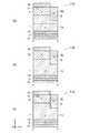
図3(a)〜図3(c)は、それぞれ、図2のA−A’断面図、B−B’断面図、及びC−C’断面図である。
図4は、図1のD−D’断面図である。
(First embodiment)
FIG. 1 is a plan view illustrating the semiconductor device according to the first embodiment.
FIG. 2 is an enlarged perspective sectional view of a portion A in FIG.
FIG. 3A to FIG. 3C are an AA ′ sectional view, a BB ′ sectional view, and a CC ′ sectional view, respectively, in FIG. 2.
4 is a cross-sectional view taken along the line DD ′ of FIG.
半導体装置100は、RC−IGBTである。図1に表したように、半導体装置100は、少なくとも1つのIGBT領域R1及び少なくとも1つのダイオード領域R2を有する。例えば、ダイオード領域R2は、IGBT領域R1同士の間に位置する。IGBT領域R1は、IGBTとして機能し、半導体装置100がオン状態のときに電流を流す。ダイオード領域R2は、例えば、半導体装置100がオフ状態のときに、フリーホイールダイオードとして機能する。
The
半導体装置100の上面には、例えば、エミッタ電極32(第2電極)、ゲートパッド33、及びゲート配線34が設けられている。エミッタ電極32は、IGBT領域R1及びダイオード領域R2の上に設けられている。ゲートパッド33及びゲート配線34は、エミッタ電極32と離間している。ゲート配線34は、ゲートパッド33と接続され、エミッタ電極32の周りに設けられている。
On the upper surface of the
図2に表したように、半導体装置100は、n−形(第1導電形)ドリフト領域1(第1半導体領域)、p+形(第2導電形)コレクタ領域2(第2半導体領域)、p形ベース領域3(第3半導体領域)、n+形エミッタ領域4(第4半導体領域)、n+形カソード領域5(第5半導体領域)、p−形アノード領域6(第6半導体領域)、p形半導体領域7a(第7半導体領域の一例)、p−形半導体領域7b(第7半導体領域の別の一例)、p+形ガードリング領域8(第8半導体領域)、p+形コンタクト領域11、p+形アノード領域12、n形バッファ領域13、ゲート電極20、ゲート絶縁層21、第1導電部24、第1絶縁層25、第2導電部28、第2絶縁層29、及びコレクタ電極31(第1電極)をさらに有する。
As shown in FIG. 2, the
実施形態の説明では、XYZ直交座標系を用いる。p+形コレクタ領域2からp形ベース領域3に向かう方向をZ方向(第2方向)とする。Z方向に対して垂直であり、相互に直交する2方向をX方向(第1方向)及びY方向(第3方向)とする。また、説明のために、p+形コレクタ領域2からp形ベース領域3に向かう方向を「上」と言い、その反対方向を「下」と言う。これらの方向は、p+形コレクタ領域2とp形ベース領域3との相対的な位置関係に基づき、重力の方向とは無関係である。
In the description of the embodiment, an XYZ orthogonal coordinate system is used. A direction from the p + -type collector region 2 to the p-
n−形ドリフト領域1は、第1部分1a、第2部分1b、及び第3部分1cを有する。第3部分1cは、X方向において第1部分1aと第2部分1bとの間に位置する。p+形コレクタ領域2は、第1部分1aの下及び第3部分1cの一部の下に設けられている。n+形カソード領域5は、第2部分1bの下及び第3部分1cの別の一部の下に設けられている。
The n − -
n−形ドリフト領域1とp+形コレクタ領域2との間及びn−形ドリフト領域1とn+形カソード領域5との間には、例えば、n形バッファ領域13が設けられている。コレクタ電極31は、p+形コレクタ領域2及びn+形カソード領域5の下に設けられ、p+形コレクタ領域2及びn+形カソード領域5と電気的に接続されている。
For example, an n-
p形ベース領域3及びゲート電極20は、第1部分1aの上に設けられている。n+形エミッタ領域4及びp+形コンタクト領域11は、p形ベース領域3の上に設けられている。ゲート電極20は、X方向において、n−形ドリフト領域1の一部、p形ベース領域3、及びn+形エミッタ領域4の少なくとも一部と、ゲート絶縁層21を介して対向している。
The p-
p−形アノード領域6及び第2導電部28は、第2部分1bの上に設けられている。p+形アノード領域12は、p−形アノード領域6の上に選択的に設けられている。第2導電部28は、X方向において、n−形ドリフト領域1の一部及びp−形アノード領域6と、第2絶縁層29を介して対向している。
The p − -
p形半導体領域7a及びp−形半導体領域7bは、第3部分1cの上に設けられている。例えば、p形半導体領域7aはp+形コレクタ領域2の直上に位置し、p−形半導体領域7bはn+形カソード領域5の直上に位置している。p+形アノード領域12が、p−形半導体領域7bの上に設けられていても良い。第1導電部24は、X方向においてp形半導体領域7a及びp−形半導体領域7bとの間に位置し、これらの半導体領域と第1絶縁層25を介して対向している。p形半導体領域7aは、X方向においてゲート電極20と第1導電部24との間に位置し、Y方向に延びている。p−形半導体領域7bは、X方向において第1導電部24と第2導電部28との間に位置し、Y方向に延びている。
The p-
エミッタ電極32は、p形ベース領域3、n+形エミッタ領域4、p+形コンタクト領域11、p形半導体領域7a、p−形半導体領域7b、p−形アノード領域6、p+形アノード領域12、p+形ガードリング領域8、第1導電部24、及び第2導電部28の上に設けられ、これらと電気的に接続されている。ゲート電極20は、ゲート配線34を介してゲートパッド33と電気的に接続されている。ゲート電極20は、エミッタ電極32と電気的に分離されている。
The
p形ベース領域3、n+形エミッタ領域4、p+形コンタクト領域11、p−形アノード領域6、ゲート電極20、第1導電部24、及び第2導電部28のそれぞれは、例えば、X方向において複数設けられ、Y方向に延びている。p+形アノード領域12は、例えば、それぞれのp−形アノード領域6の上において、Y方向に複数設けられている。p形半導体領域7a及びp−形半導体領域7bは、Y方向に延びている。
Each of the p-
図1では、p+形ガードリング領域8の外縁を破線で表している。p+形ガードリング領域8は、複数のp形ベース領域3、複数のp−形アノード領域6、p形半導体領域7a、及びp−形半導体領域7bを囲んでいる。p+形ガードリング領域8は、図2に表したように、第1領域8a、第2領域8b、及び第3領域8cを有する。
In FIG. 1, the outer edge of the p + -type
図3(a)に表したように、第1領域8aの一部は、Y方向においてp形ベース領域3と並んでいる。図3(b)に表したように、第2領域8bの一部は、Y方向においてp形半導体領域7aと並んでいる。第2領域8bの別の一部は、Y方向においてp−形半導体領域7bと並んでいる。図3(c)に表したように、第3領域8cの一部は、Y方向においてp−形アノード領域6と並んでいる。
As shown in FIG. 3A, a part of the
第2領域8bの下端は、第1領域8aの下端及び第3領域8cの下端よりも上方に位置する。すなわち、第2領域8bとn−形ドリフト領域1とのpn接合面は、第1領域8aとn−形ドリフト領域1とのpn接合面及び第3領域8cとn−形ドリフト領域1とのpn接合面よりも上方に位置する。
The lower end of the
p+形ガードリング領域8の下端の位置は、例えば図4(a)に表したように、連続的に変化している。または、p+形ガードリング領域8の下端の位置は、図4(b)に表したように、ステップ状に変化していても良い。例えば、第1領域8aの最も深い深さ(最も長いZ方向における長さ)D1は、ゲート絶縁層21、第1絶縁層25、または第2絶縁層29の深さD(図2に表す)の、1.0倍以上2.0倍以下であることが望ましい。深さDは、換言すると、これらの絶縁層の下端とソース電極32との間のZ方向における距離である。第2領域8bの最も浅い深さ(最も短いZ方向における長さ)D2は、Dより大きく、D1未満である。第3領域8cの下端は、例えば、第2領域8bの下端よりも下方に位置する。または、第3領域8cの下端は、第2領域8bの下端と同じ位置にあっても良い。
The position of the lower end of the p + -type
半導体装置100の動作を説明する。
コレクタ電極31に、エミッタ電極32に対して正の電圧が印加された状態で、ゲート電極20に閾値以上の電圧が印加されると、半導体装置100がオン状態となる。このとき、p形ベース領域3のゲート絶縁層21近傍の領域にチャネル(反転層)が形成される。電子は、このチャネルを通ってn+形エミッタ領域4からn−形ドリフト領域1に注入され、正孔は、p+形コレクタ領域2からn−形ドリフト領域1に注入される。これにより、IGBT領域R1に電流が流れる。その後、ゲート電極20に印加される電圧が閾値よりも低くなると、p形ベース領域3におけるチャネルが消滅し、半導体装置100がオフ状態になる。
The operation of the
When a positive voltage is applied to the
例えば、複数の半導体装置100によってブリッジ回路が構成されている場合、1つの半導体装置100がオン状態からオフ状態に切り替わると、ブリッジ回路のインダクタンス成分により、別の半導体装置100のエミッタ電極32に誘導起電力が加わる。これにより、この別の半導体装置100において、ダイオード領域R2が動作し、p−形アノード領域6(p+形アノード領域12)からn−形ドリフト領域1へ正孔が注入され、n+形カソード領域5からn−形ドリフト領域1へ電子が注入される。
For example, when a bridge circuit is configured by a plurality of
半導体装置100の各構成要素の材料の一例を説明する。
n−形ドリフト領域1、p+形コレクタ領域2、p形ベース領域3、n+形エミッタ領域4、n+形カソード領域5、p−形アノード領域6、p形半導体領域7a、p−形半導体領域7b、p+形ガードリング領域8、p+形コンタクト領域11、p+形アノード領域12、及びn形バッファ領域13は、半導体材料として、シリコン、炭化シリコン、窒化ガリウム、またはガリウムヒ素を含む。半導体材料としてシリコンが用いられる場合、n形不純物として、ヒ素、リン、またはアンチモンを用いることができる。p形不純物として、ボロンを用いることができる。
ゲート電極20、第1導電部24、及び第2導電部28は、ポリシリコンなどの導電材料を含む。
ゲート絶縁層21、第1絶縁層25、及び第2絶縁層29は、酸化シリコンなどの絶縁材料を含む。
コレクタ電極31、エミッタ電極32、ゲートパッド33、及びゲート配線34は、アルミニウムなどの金属を含む。
An example of the material of each component of the
n − -
The
The
The
第1実施形態の効果を説明する。
半導体装置100がオン状態からオフ状態に切り替わると、半導体装置100が接続された電気回路のインダクタンス成分により、コレクタ電極31に誘導起電力が加わる場合がある。コレクタ電極31に誘導起電力が加わると、IGBT領域R1内部において、アバランシェ降伏が生じる。一般的に、アバランシェ降伏は、IGBT領域R1において局所的に発生し、これにより、IGBT領域R1を流れる電流フィラメントが発生する。電流フィラメントが発生すると、その箇所の温度が上昇する。従って、同じ箇所で電流フィラメントが発生し続けると、最終的に熱暴走によって半導体装置100が破壊されてしまう。
The effect of the first embodiment will be described.
When the
発明者は、RC−IGBTにおいて、電流フィラメントによる破壊が、IGBT領域R1とダイオード領域R2との境界の近傍であり、且つp+形ガードリング領域8近傍の部分において、特に発生しやすいことを発見した。発明者は、この知見に基づき検討を行ったところ、当該部分における電界を、IGBT領域R1のp+形ガードリング領域8近傍の電界よりも低くすることで、電流フィラメントによる破壊が発生し難くなることを発見した。
The inventor found that in the RC-IGBT, the breakdown due to the current filament is particularly likely to occur near the boundary between the IGBT region R1 and the diode region R2 and in the vicinity of the p + -type
半導体装置100では、n−形ドリフト領域1は、IGBT領域R1に含まれる第1部分1aと、ダイオード領域R2に含まれる第2部分1bと、の間に位置する第3部分1cを有する。第3部分1cの上には、p形半導体領域7a及びp−形半導体領域7bが設けられ、p+形ガードリング領域8の第2領域8bの一部は、p形半導体領域7a及びp−形半導体領域7bとY方向において並んでいる。この第2領域8bの下端は、p形ベース領域3とY方向において並ぶ第1領域8aの下端よりも上方に位置する。この構成によれば、従来の半導体装置において電流フィラメントによる破壊が生じ易い箇所の電界を低減でき、当該箇所で破壊が発生する可能性を低減できる。
In
(変形例)
図5は、第1実施形態の変形例に係る半導体装置の一部を表す断面図である。
図6は、第1実施形態の変形例に係る半導体装置の特性を表すグラフである。
(Modification)
FIG. 5 is a cross-sectional view illustrating a part of a semiconductor device according to a modification of the first embodiment.
FIG. 6 is a graph showing characteristics of the semiconductor device according to the modification of the first embodiment.
変形例に係る半導体装置110は、半導体装置100と、p+形ガードリング領域8の構造が異なる。図5(a)〜図5(c)は、それぞれ、図2のA−A’断面図、B−B’断面図、及びC−C’断面図に対応する。図5(a)〜図5(c)に表したように、半導体装置110では、第1領域8a〜第3領域8cのそれぞれの下端が同じ位置にある。
The
図6の横軸は、X方向における位置Pを表し、縦軸は、p+形ガードリング領域8の各点のp形不純物濃度C[atoms/cm3]を表す。図6に表したように、第2領域8bにおけるp形不純物濃度は、第1領域8aにおけるp形不純物濃度よりも低い。例えば、第1領域8aにおけるピークのp形不純物濃度C1は、第2領域8bにおける最も低いp形不純物濃度C2の、1.1倍以上、10倍以下であることが望ましい。
The horizontal axis in FIG. 6 represents the position P in the X direction, and the vertical axis represents the p-type impurity concentration C [atoms / cm 3 ] at each point of the p + -type
第3領域8cにおけるp形不純物濃度は、例えば、第2領域8bにおけるp形不純物濃度よりも高い。または、第3領域8cにおけるp形不純物濃度は、第2領域8bにおけるp形不純物濃度と同じでも良い。
For example, the p-type impurity concentration in the
第2領域8bにおけるp形不純物濃度が第1領域8aにおけるp形不純物濃度よりも低いことで、半導体装置100と同様に、第2領域8b近傍における電界強度を、第1領域8a近傍における電界強度よりも低減できる。これにより、半導体装置100と同様に、電流フィラメントによる破壊が発生する可能性を低減できる。
Since the p-type impurity concentration in the
なお、半導体装置110において、半導体装置100と同様に、第2領域8bの下端を、第1領域8aの下端よりも上方に位置させても良い。これにより、第2領域8b近傍における電界強度をより低減できる。
In the
(第2実施形態)
図7は、第2実施形態に係る半導体装置を表す斜視断面図である。
第2実施形態に係る半導体装置200は、ゲート電極20の構造について、半導体装置100と差異を有する。
(Second Embodiment)
FIG. 7 is a perspective sectional view showing a semiconductor device according to the second embodiment.
The
半導体装置200では、第1絶縁層25の下端及び第2絶縁層29の下端が、ゲート絶縁層21の下端よりも上方に位置している。すなわち、第1導電部24の下端及び第2導電部28の下端が、ゲート電極20の下端よりも上方に位置している。第1導電部24及び第2導電部28のそれぞれのZ方向における長さは、ゲート電極20のZ方向における長さよりも短い。
In the
複数のゲート電極20は、ゲート電極20a、20b、及び20cを含む。ゲート電極20bの下端の位置は、ゲート電極20aの下端の位置よりも上方に位置し、ゲート電極20cの下端の位置よりも下方に位置している。ゲート電極20cは、X方向において、p形ベース領域3とp形半導体領域7aとの間及びゲート電極20bと第1導電部24との間に位置している。ゲート電極20bは、ゲート電極20aよりもp形半導体領域7a側に位置している。換言すると、ゲート電極20の下端の位置は、p形半導体領域7a(ダイオード領域R2)に近づくほど、より上方に位置している。
The plurality of
IGBT領域R1とダイオード領域R2との境界近傍に設けられたゲート電極20cの下端の位置を、IGBT領域R1の中心側に設けられたゲート電極20a及び20bの下端の位置よりも上方に位置させることで、境界近傍の電界強度を低減できる。これにより、第2領域8b近傍における電界強度も低減され、電流フィラメントによる破壊が発生する可能性を低減できる。
The position of the lower end of the
望ましくは、ゲート電極20bの下端の位置は、ゲート電極20aの下端の位置よりも情報に位置する。このように、IGBT領域R1内において、ダイオード領域R2に近づくほど、ゲート電極20の下端の位置を上方に位置させることで、IGBT領域R1とダイオード領域R2との境界近傍における電界強度をより一層低減できる。
Desirably, the position of the lower end of the
(第3実施形態)
図8は、第3実施形態に係る半導体装置を表す斜視断面図である。
第3実施形態に係る半導体装置300は、n形バリア領域9(第9半導体領域)をさらに有する。n形バリア領域9は、X方向において複数設けられている。複数のn形バリア領域9は、それぞれ、Z方向において、第1部分1aと複数のp形ベース領域3との間に設けられている。
(Third embodiment)
FIG. 8 is a perspective sectional view showing a semiconductor device according to the third embodiment.
The
複数のn形バリア領域9は、n形バリア領域9a及びn形バリア領域9bを含む。n形バリア領域9bのn形不純物濃度は、n形バリア領域9aのn形不純物濃度よりも低い。n形バリア領域9bのX方向における位置は、p形半導体領域7aのX方向における位置と、n形バリア領域9aのX方向における位置と、の間にある。すなわち、p形半導体領域7a(ダイオード領域R2)に近づくほど、n形バリア領域9のn形不純物濃度が低い。
The plurality of n-
IGBT領域R1とダイオード領域R2との境界近傍に設けられたn形バリア領域9bのn形不純物濃度を、IGBT領域R1の中心側に設けられたn形バリア領域9aのn形不純物濃度よりも低くすることで、境界近傍の電界強度を低減できる。これにより、第2領域8b近傍における電界強度も低減され、電流フィラメントによる破壊が発生する可能性を低減できる。
The n-type impurity concentration of the n-type barrier region 9b provided in the vicinity of the boundary between the IGBT region R1 and the diode region R2 is lower than the n-type impurity concentration of the n-
望ましくは、n形バリア領域9aのn形不純物濃度は、n形バリア領域9aよりもIGBT領域R1の中心側に設けられた、別のn形バリア領域9のn形不純物濃度よりも低い。このように、IGBT領域R1内において、ダイオード領域R2に近づくほど、n形バリア領域9の濃度を低下させることで、IGBT領域R1とダイオード領域R2との境界近傍における電界強度をより一層低減できる。
Desirably, the n-type impurity concentration of n-
なお、本実施形態におけるn形バリア領域9同士の間のn形不純物濃度の高低について、n形バリア領域9にp形不純物とn形不純物の両方が含まれている場合には、それらの不純物が補償しあった後の正味の不純物濃度の相対的な高低が、上述した関係にあれば良い。
In addition, regarding the level of n-type impurity concentration between the n-
(第4実施形態)
図9は、第4実施形態に係る半導体装置を表す斜視断面図である。
図9に表したように、複数のゲート電極20は、ゲート電極20a、ゲート電極20b、及びゲート電極20cを含む。複数のゲート絶縁層21は、ゲート絶縁層21a、ゲート絶縁層21b、及びゲート絶縁層21cを含む。
(Fourth embodiment)
FIG. 9 is a perspective sectional view showing a semiconductor device according to the fourth embodiment.
As shown in FIG. 9, the plurality of
第4実施形態に係る半導体装置400では、第1絶縁層25と、第1絶縁層25とX方向において隣り合うゲート絶縁層21cと、の間の距離D3が、X方向において隣り合うゲート絶縁層21bとゲート絶縁層21cとの間の距離D4よりも短い。これに伴い、第1導電部24と、第1導電部24とX方向において隣り合うゲート電極20cと、の間の距離D6が、X方向において隣り合うゲート電極20bとゲート電極20cとの間の距離D7よりも短い。
In the
また、距離D4は、ゲート絶縁層21aとゲート絶縁層21bとの間のX方向における距離D5よりも短い。これに伴い、距離D7は、ゲート電極20aとゲート電極20bとの間のX方向における距離D8よりも短い。
The distance D4 is shorter than the distance D5 in the X direction between the
また、上記の構成に伴い、p形半導体領域7aのX方向における長さL1は、p形半導体領域7aに隣り合うp形ベース領域3bのX方向における長さL2よりも短い。p形ベース領域3bの長さL2は、p形ベース領域3aのX方向における長さL3よりも短い。
With the above configuration, the length L1 of the p-
この構成によれば、他の実施形態と同様に、境界近傍の電界強度を低減できる。これにより、第2領域8b近傍における電界強度を低減でき、電流フィラメントによる破壊が発生する可能性を低減できる。
According to this configuration, the electric field strength in the vicinity of the boundary can be reduced as in the other embodiments. Thereby, the electric field strength in the vicinity of the
望ましくは、距離D5は、よりIGBT領域R1の中心側に設けられた、隣り合うゲート絶縁層21同士の間のX方向における距離よりも短い。距離D8は、よりIGBT領域R1の中心側に設けられた、隣り合うゲート電極20同士の間のX方向における距離よりも短い。長さL3は、よりIGBT領域R1の中心側に設けられた、別のp形ベース領域3のX方向における長さよりも短い。このような構成によれば、IGBT領域R1とダイオード領域R2との境界近傍における電界強度をより一層低減できる。
Desirably, the distance D5 is shorter than the distance in the X direction between adjacent
以上で説明した各実施形態における、各半導体領域の間の不純物濃度の相対的な高低については、例えば、SCM(走査型静電容量顕微鏡)を用いて確認することが可能である。なお、各半導体領域におけるキャリア濃度は、各半導体領域において活性化している不純物濃度と等しいものとみなすことができる。従って、各半導体領域の間のキャリア濃度の相対的な高低についても、SCMを用いて確認することができる。
また、各半導体領域における不純物濃度については、例えば、SIMS(二次イオン質量分析法)により測定することが可能である。
The relative level of the impurity concentration between the semiconductor regions in each of the embodiments described above can be confirmed using, for example, an SCM (scanning capacitance microscope). The carrier concentration in each semiconductor region can be regarded as being equal to the impurity concentration activated in each semiconductor region. Therefore, the relative level of the carrier concentration between the semiconductor regions can also be confirmed using the SCM.
The impurity concentration in each semiconductor region can be measured by, for example, SIMS (secondary ion mass spectrometry).
以上、本発明のいくつかの実施形態を例示したが、これらの実施形態は、例として提示したものであり、発明の範囲を限定することは意図していない。これら新規な実施形態は、その他の様々な形態で実施されることが可能であり、発明の要旨を逸脱しない範囲で、種々の省略、置き換え、変更などを行うことができる。これら実施形態やその変形例は、発明の範囲や要旨に含まれるとともに、特許請求の範囲に記載された発明とその均等の範囲に含まれる。また、前述の各実施形態は、相互に組み合わせて実施することができる。 As mentioned above, although several embodiment of this invention was illustrated, these embodiment is shown as an example and is not intending limiting the range of invention. These novel embodiments can be implemented in various other forms, and various omissions, replacements, changes, and the like can be made without departing from the spirit of the invention. These embodiments and modifications thereof are included in the scope and gist of the invention, and are included in the invention described in the claims and equivalents thereof. Further, the above-described embodiments can be implemented in combination with each other.
1 n−形ドリフト領域、 1a 第1部分、 1b 第2部分、 1c 第3部分、 2 p+形コレクタ領域、 3、3a、3b p形ベース領域、 4 n+形エミッタ領域、 5 n+形カソード領域、 6 p−形アノード領域、 7a p形半導体領域、 7b p−形半導体領域、 8 p+形ガードリング領域、 8a 第1領域、 8b 第2領域、 8c 第3領域、 9、9a、9b n形バリア領域、 11 p+形コンタクト領域、 12 p+形アノード領域、 13 n形バッファ領域、 20、20a、20b、20c ゲート電極、 21、21a、21b、21c ゲート絶縁層、 24 第1導電部、 25 第1絶縁層、 28 第2導電部、 29 第2絶縁層、 31 コレクタ電極、 32 エミッタ電極、 33 ゲートパッド、 34 ゲート配線、 100、110、200、300、400 半導体装置、 R1 IGBT領域、 R2 ダイオード領域 1 n − type drift region, 1a first part, 1b second part, 1c third part, 2 p + type collector region, 3, 3a, 3b p type base region, 4 n + type emitter region, 5 n + type Cathode region, 6 p − type anode region, 7a p type semiconductor region, 7b p − type semiconductor region, 8 p + type guard ring region, 8a first region, 8b second region, 8c third region, 9, 9a, 9b n-type barrier region, 11 p + type contact region, 12 p + type anode region, 13 n type buffer region, 20, 20a, 20b, 20c gate electrode, 21, 21a, 21b, 21c gate insulating layer, 24 1st Conductive portion, 25 First insulating layer, 28 Second conductive portion, 29 Second insulating layer, 31 Collector electrode, 32 Emitter electrode, 33 Gate pad, 34 Gate wiring, 100, 11 0, 200, 300, 400 Semiconductor device, R1 IGBT region, R2 diode region
Claims (11)
前記第1部分の下に設けられた第2導電形の第2半導体領域と、
前記第1部分の上に設けられた第2導電形の第3半導体領域であって、前記第2半導体領域から前記第3半導体領域に向かう第2方向は前記第1方向に対して垂直である、前記第3半導体領域と、
前記第3半導体領域の上に設けられた第1導電形の第4半導体領域と、
前記第1方向において、前記第1半導体領域の一部、前記第3半導体領域、及び前記第4半導体領域の少なくとも一部とゲート絶縁層を介して対向するゲート電極と、
前記第2部分の下に設けられた第1導電形の第5半導体領域と、
前記第2部分の上に設けられた第2導電形の第6半導体領域と、
前記第3部分の上に設けられた第2導電形の第7半導体領域と、
前記第3半導体領域、前記第6半導体領域、及び前記第7半導体領域を囲む第2導電形の第8半導体領域であって、前記第8半導体領域は、
前記第1方向及び前記第2方向に垂直な第3方向において、一部が前記第3半導体領域と並ぶ第1領域と、
前記第3方向において、一部が前記第7半導体領域と並ぶ第2領域と、
を有し、前記第2領域の下端は前記第1領域の下端よりも上方に位置する、前記第8半導体領域と、
を備えた半導体装置。 A first conductivity type first semiconductor region having a first portion, a second portion, and a third portion located between the first portion and the second portion in the first direction;
A second semiconductor region of a second conductivity type provided under the first portion;
A second semiconductor region of a second conductivity type provided on the first portion, wherein a second direction from the second semiconductor region toward the third semiconductor region is perpendicular to the first direction; The third semiconductor region;
A fourth semiconductor region of a first conductivity type provided on the third semiconductor region;
A gate electrode opposed to at least a part of the first semiconductor region, the third semiconductor region, and the fourth semiconductor region via a gate insulating layer in the first direction;
A fifth semiconductor region of a first conductivity type provided under the second portion;
A sixth semiconductor region of a second conductivity type provided on the second portion;
A seventh semiconductor region of a second conductivity type provided on the third portion;
An eighth semiconductor region of a second conductivity type surrounding the third semiconductor region, the sixth semiconductor region, and the seventh semiconductor region, wherein the eighth semiconductor region is:
A first region partially aligned with the third semiconductor region in a third direction perpendicular to the first direction and the second direction;
A second region partially aligned with the seventh semiconductor region in the third direction;
And the lower end of the second region is located above the lower end of the first region, the eighth semiconductor region,
A semiconductor device comprising:
複数の前記ゲート電極の1つは、前記第1方向において、前記第7半導体領域と前記複数のゲート電極の別の1つとの間に位置し、
前記複数のゲート電極の前記1つの下端は、前記複数のゲート電極の前記別の1つの下端よりも上方に位置している請求項1または2に記載の半導体装置。 A plurality of the gate electrodes;
One of the plurality of gate electrodes is located between the seventh semiconductor region and another one of the plurality of gate electrodes in the first direction;
3. The semiconductor device according to claim 1, wherein the lower end of the plurality of gate electrodes is located above the lower end of the other one of the plurality of gate electrodes.
前記第1導電部の下端は、前記複数のゲート電極のそれぞれの下端よりも上方に位置している請求項3記載の半導体装置。 A first conductive portion facing the seventh semiconductor region in the first direction through a first insulating layer and electrically connected to the second electrode;
4. The semiconductor device according to claim 3, wherein a lower end of the first conductive portion is located above a lower end of each of the plurality of gate electrodes.
第1導電形の複数の第9半導体領域と、
を備え、
前記複数の第9半導体領域は、それぞれ、前記複数の第3半導体領域と前記第1部分との間に設けられ、
前記複数の第9半導体領域のそれぞれにおける第1導電形の不純物濃度は、前記第1半導体領域における第1導電形の不純物濃度よりも高く、
前記複数の第9半導体領域の1つの前記第1方向における位置は、前記第7半導体領域の前記第1方向における位置と、前記複数の第3半導体領域の別の1つの前記第1方向における位置と、の間にあり、
前記複数の第9半導体領域の前記1つにおける第1導電形の不純物濃度は、前記複数の第9半導体領域の前記別の1つにおける第1導電形の不純物濃度よりも低い請求項1〜6のいずれか1つに記載の半導体装置。 A plurality of the third semiconductor regions;
A plurality of ninth semiconductor regions of the first conductivity type;
With
The plurality of ninth semiconductor regions are provided between the plurality of third semiconductor regions and the first portion, respectively.
The impurity concentration of the first conductivity type in each of the plurality of ninth semiconductor regions is higher than the impurity concentration of the first conductivity type in the first semiconductor region,
The position of one of the plurality of ninth semiconductor regions in the first direction is the position of the seventh semiconductor region in the first direction and the position of another one of the plurality of third semiconductor regions in the first direction. And between
The impurity concentration of the first conductivity type in the one of the plurality of ninth semiconductor regions is lower than the impurity concentration of the first conductivity type in the another one of the plurality of ninth semiconductor regions. The semiconductor device according to any one of the above.
前記第1部分の下に設けられた第2導電形の第2半導体領域と、
前記第1部分の上に設けられた第2導電形の第3半導体領域であって、前記第2半導体領域から前記第3半導体領域に向かう第2方向は前記第1方向に対して垂直である、前記第3半導体領域と、
前記第3半導体領域の上に設けられた第1導電形の第4半導体領域と、
前記第1方向において、前記第1半導体領域の一部、前記第3半導体領域、及び前記第4半導体領域の少なくとも一部とゲート絶縁層を介して対向するゲート電極と、
前記第2部分の下に設けられた第1導電形の第5半導体領域と、
前記第2部分の上に設けられた第2導電形の第6半導体領域と、
前記第3部分の上に設けられた第2導電形の第7半導体領域と、
前記第3半導体領域、前記第6半導体領域、及び前記第7半導体領域を囲む第2導電形の第8半導体領域であって、前記第8半導体領域は、
前記第1方向及び前記第2方向に垂直な第3方向において、一部が前記第3半導体領域と並ぶ第1領域と、
前記第3方向において、一部が前記第7半導体領域と並ぶ第2領域と、
を有し、前記第2領域における第2導電形の不純物濃度は、前記第1領域における第2導電形の不純物濃度よりも高い、前記第8半導体領域と、
を備えた半導体装置。 A first conductivity type first semiconductor region having a first portion, a second portion, and a third portion located between the first portion and the second portion in the first direction;
A second semiconductor region of a second conductivity type provided under the first portion;
A second semiconductor region of a second conductivity type provided on the first portion, wherein a second direction from the second semiconductor region toward the third semiconductor region is perpendicular to the first direction; The third semiconductor region;
A fourth semiconductor region of a first conductivity type provided on the third semiconductor region;
A gate electrode opposed to at least a part of the first semiconductor region, the third semiconductor region, and the fourth semiconductor region via a gate insulating layer in the first direction;
A fifth semiconductor region of a first conductivity type provided under the second portion;
A sixth semiconductor region of a second conductivity type provided on the second portion;
A seventh semiconductor region of a second conductivity type provided on the third portion;
An eighth semiconductor region of a second conductivity type surrounding the third semiconductor region, the sixth semiconductor region, and the seventh semiconductor region, wherein the eighth semiconductor region is:
A first region partially aligned with the third semiconductor region in a third direction perpendicular to the first direction and the second direction;
A second region partially aligned with the seventh semiconductor region in the third direction;
An impurity concentration of the second conductivity type in the second region is higher than an impurity concentration of the second conductivity type in the first region; and
A semiconductor device comprising:
前記第1部分の下に設けられた第2導電形の第2半導体領域と、
前記第1部分の上に設けられた第2導電形の複数の第3半導体領域であって、前記第2半導体領域から前記複数の第3半導体領域に向かう第2方向は前記第1方向に対して垂直である、前記複数の第3半導体領域と、
前記複数の第3半導体領域の1つの上に設けられた第1導電形の第4半導体領域と、
前記第1方向において、前記第1半導体領域の一部、前記複数の第3半導体領域の前記1つ、及び前記第4半導体領域の少なくとも一部とゲート絶縁層を介して対向するゲート電極と、
前記第2部分の下に設けられた第1導電形の第5半導体領域と、
前記第2部分の上に設けられた第2導電形の第6半導体領域と、
前記第3部分の上に設けられた第2導電形の第7半導体領域と、
前記複数の第3半導体領域、前記第6半導体領域、及び前記第7半導体領域を囲む第2導電形の第8半導体領域と、
複数の第9半導体領域であって、前記複数の第9半導体領域はそれぞれ前記複数の第3半導体領域と前記第1部分との間に設けられ、前記複数の第9半導体領域のそれぞれにおける第1導電形の不純物濃度は、前記第1半導体領域における第1導電形の不純物濃度よりも高く、前記複数の第9半導体領域の1つの前記第1方向における位置は、前記第7半導体領域の前記第1方向における位置と、前記複数の第3半導体領域の別の1つの前記第1方向における位置と、の間にあり、前記複数の第9半導体領域の前記1つにおける第1導電形の不純物濃度は、前記複数の第9半導体領域の前記別の1つにおける第1導電形の不純物濃度よりも低い、前記複数の第9半導体領域と、
を備えた半導体装置。 A first conductivity type first semiconductor region having a first portion, a second portion, and a third portion located between the first portion and the second portion in the first direction;
A second semiconductor region of a second conductivity type provided under the first portion;
A plurality of third semiconductor regions of a second conductivity type provided on the first portion, wherein a second direction from the second semiconductor region toward the plurality of third semiconductor regions is relative to the first direction; A plurality of third semiconductor regions that are perpendicular to each other;
A fourth semiconductor region of a first conductivity type provided on one of the plurality of third semiconductor regions;
A gate electrode facing a part of the first semiconductor region, the one of the plurality of third semiconductor regions, and at least a part of the fourth semiconductor region through a gate insulating layer in the first direction;
A fifth semiconductor region of a first conductivity type provided under the second portion;
A sixth semiconductor region of a second conductivity type provided on the second portion;
A seventh semiconductor region of a second conductivity type provided on the third portion;
An eighth semiconductor region of a second conductivity type surrounding the plurality of third semiconductor regions, the sixth semiconductor region, and the seventh semiconductor region;
A plurality of ninth semiconductor regions, wherein the plurality of ninth semiconductor regions are provided between the plurality of third semiconductor regions and the first portion, respectively, and the first in each of the plurality of ninth semiconductor regions. The impurity concentration of the conductivity type is higher than the impurity concentration of the first conductivity type in the first semiconductor region, and the position of one of the plurality of ninth semiconductor regions in the first direction is the first concentration of the seventh semiconductor region. An impurity concentration of the first conductivity type in the one of the plurality of ninth semiconductor regions, which is between a position in one direction and a position in another one of the plurality of third semiconductor regions in the first direction The plurality of ninth semiconductor regions having a lower impurity concentration of the first conductivity type in the other one of the plurality of ninth semiconductor regions;
A semiconductor device comprising:
前記第1部分の下に設けられた第2導電形の第2半導体領域と、
前記第1部分の上に設けられた第2導電形の第3半導体領域であって、前記第2半導体領域から前記第3半導体領域に向かう第2方向は前記第1方向に対して垂直である、前記第3半導体領域と、
前記第3半導体領域の上に設けられた第1導電形の第4半導体領域と、
前記第1方向において、前記第1半導体領域の一部、前記第3半導体領域、及び前記第4半導体領域の少なくとも一部とゲート絶縁層を介して対向するゲート電極と、
前記第2部分の下に設けられた第1導電形の第5半導体領域と、
前記第2部分の上に設けられた第2導電形の第6半導体領域と、
前記第3部分の上に設けられた第2導電形の第7半導体領域と、
前記第1方向において、前記第7半導体領域と第1絶縁層を介して対向する第1導電部であって、前記第1導電部の下端は前記ゲート電極の下端よりも上方に位置する、前記第1導電部と、
前記第3半導体領域、前記第6半導体領域、及び前記第7半導体領域を囲む第2導電形の第8半導体領域と、
を備えた半導体装置。 A first conductivity type first semiconductor region having a first portion, a second portion, and a third portion located between the first portion and the second portion in the first direction;
A second semiconductor region of a second conductivity type provided under the first portion;
A second semiconductor region of a second conductivity type provided on the first portion, wherein a second direction from the second semiconductor region toward the third semiconductor region is perpendicular to the first direction; The third semiconductor region;
A fourth semiconductor region of a first conductivity type provided on the third semiconductor region;
A gate electrode opposed to at least a part of the first semiconductor region, the third semiconductor region, and the fourth semiconductor region via a gate insulating layer in the first direction;
A fifth semiconductor region of a first conductivity type provided under the second portion;
A sixth semiconductor region of a second conductivity type provided on the second portion;
A seventh semiconductor region of a second conductivity type provided on the third portion;
A first conductive portion facing the seventh semiconductor region via a first insulating layer in the first direction, wherein a lower end of the first conductive portion is located above a lower end of the gate electrode; A first conductive part;
An eighth semiconductor region of a second conductivity type surrounding the third semiconductor region, the sixth semiconductor region, and the seventh semiconductor region;
A semiconductor device comprising:
前記第1部分の下に設けられた第2導電形の第2半導体領域と、
前記第1部分の上に設けられた第2導電形の第3半導体領域であって、前記第2半導体領域から前記第3半導体領域に向かう第2方向は前記第1方向に対して垂直である、前記第3半導体領域と、
前記第3半導体領域の上に設けられた第1導電形の第4半導体領域と、
複数のゲート電極であって、前記複数のゲート電極の1つは、前記第1方向において、前記第1半導体領域の一部、前記第3半導体領域、及び前記第4半導体領域の少なくとも一部とゲート絶縁層を介して対向する、前記複数のゲート電極と、
前記第2部分の下に設けられた第1導電形の第5半導体領域と、
前記第2部分の上に設けられた第2導電形の第6半導体領域と、
前記第3部分の上に設けられた第2導電形の第7半導体領域と、
前記第1方向において前記第7半導体領域と第1絶縁層を介して対向する第1導電部であって、前記第1導電部と、前記第1方向において前記第1導電部と隣り合う前記複数のゲート電極の1つと、の間の距離は、前記第1方向において隣り合う前記ゲート電極同士の間の距離よりも短い、前記第1導電部と、
前記第3半導体領域、前記第6半導体領域、及び前記第7半導体領域を囲む第2導電形の第8半導体領域と、
を備えた半導体装置。 A first conductivity type first semiconductor region having a first portion, a second portion, and a third portion located between the first portion and the second portion in the first direction;
A second semiconductor region of a second conductivity type provided under the first portion;
A second semiconductor region of a second conductivity type provided on the first portion, wherein a second direction from the second semiconductor region toward the third semiconductor region is perpendicular to the first direction; The third semiconductor region;
A fourth semiconductor region of a first conductivity type provided on the third semiconductor region;
A plurality of gate electrodes, wherein one of the plurality of gate electrodes includes, in the first direction, at least a part of the first semiconductor region, the third semiconductor region, and the fourth semiconductor region; A plurality of the gate electrodes facing each other through a gate insulating layer;
A fifth semiconductor region of a first conductivity type provided under the second portion;
A sixth semiconductor region of a second conductivity type provided on the second portion;
A seventh semiconductor region of a second conductivity type provided on the third portion;
A first conductive portion facing the seventh semiconductor region via a first insulating layer in the first direction, the plurality of the first conductive portions being adjacent to the first conductive portion in the first direction. A distance between one of the gate electrodes is shorter than a distance between the gate electrodes adjacent to each other in the first direction;
An eighth semiconductor region of a second conductivity type surrounding the third semiconductor region, the sixth semiconductor region, and the seventh semiconductor region;
A semiconductor device comprising:
Priority Applications (3)
| Application Number | Priority Date | Filing Date | Title |
|---|---|---|---|
| JP2018029695A JP2019145708A (en) | 2018-02-22 | 2018-02-22 | Semiconductor device |
| US16/029,799 US10727225B2 (en) | 2018-02-22 | 2018-07-09 | IGBT semiconductor device |
| CN201810767250.6A CN110190053A (en) | 2018-02-22 | 2018-07-13 | Semiconductor device |
Applications Claiming Priority (1)
| Application Number | Priority Date | Filing Date | Title |
|---|---|---|---|
| JP2018029695A JP2019145708A (en) | 2018-02-22 | 2018-02-22 | Semiconductor device |
Publications (2)
| Publication Number | Publication Date |
|---|---|
| JP2019145708A true JP2019145708A (en) | 2019-08-29 |
| JP2019145708A5 JP2019145708A5 (en) | 2020-03-19 |
Family
ID=67618164
Family Applications (1)
| Application Number | Title | Priority Date | Filing Date |
|---|---|---|---|
| JP2018029695A Pending JP2019145708A (en) | 2018-02-22 | 2018-02-22 | Semiconductor device |
Country Status (3)
| Country | Link |
|---|---|
| US (1) | US10727225B2 (en) |
| JP (1) | JP2019145708A (en) |
| CN (1) | CN110190053A (en) |
Cited By (1)
| Publication number | Priority date | Publication date | Assignee | Title |
|---|---|---|---|---|
| US11575001B2 (en) | 2020-10-01 | 2023-02-07 | Mitsubishi Electric Corporation | Semiconductor device |
Families Citing this family (8)
| Publication number | Priority date | Publication date | Assignee | Title |
|---|---|---|---|---|
| US9171843B2 (en) | 2013-08-02 | 2015-10-27 | Taiwan Semiconductor Manufacturing Company, Ltd. | Semiconductor device and fabricating the same |
| CN109979935B (en) * | 2017-12-28 | 2025-04-22 | 富士电机株式会社 | Semiconductor device and method for manufacturing semiconductor device |
| JP6935351B2 (en) * | 2018-03-20 | 2021-09-15 | 株式会社東芝 | Semiconductor device |
| JP7250473B2 (en) * | 2018-10-18 | 2023-04-03 | 三菱電機株式会社 | semiconductor equipment |
| JP7101593B2 (en) * | 2018-10-30 | 2022-07-15 | 三菱電機株式会社 | Semiconductor equipment |
| DE102019133030B4 (en) * | 2019-12-04 | 2023-05-04 | Infineon Technologies Austria Ag | INSULATED GATE BIPOLAR TRANSISTOR INCLUDING SEMICONDUCTOR DEVICE AND METHOD OF MANUFACTURE |
| JP7403401B2 (en) * | 2020-07-10 | 2023-12-22 | 三菱電機株式会社 | semiconductor equipment |
| JP7488778B2 (en) * | 2021-01-29 | 2024-05-22 | 株式会社東芝 | Semiconductor Device |
Citations (3)
| Publication number | Priority date | Publication date | Assignee | Title |
|---|---|---|---|---|
| JP2009021557A (en) * | 2007-06-14 | 2009-01-29 | Denso Corp | Semiconductor device |
| JP2017098359A (en) * | 2015-11-20 | 2017-06-01 | トヨタ自動車株式会社 | Reverse conducting IGBT |
| JP2017224685A (en) * | 2016-06-14 | 2017-12-21 | 株式会社デンソー | Semiconductor device |
Family Cites Families (12)
| Publication number | Priority date | Publication date | Assignee | Title |
|---|---|---|---|---|
| US8716746B2 (en) * | 2010-08-17 | 2014-05-06 | Denso Corporation | Semiconductor device |
| JP5664029B2 (en) | 2010-09-01 | 2015-02-04 | 株式会社デンソー | Semiconductor device |
| JP5321669B2 (en) * | 2010-11-25 | 2013-10-23 | 株式会社デンソー | Semiconductor device |
| WO2012169053A1 (en) | 2011-06-09 | 2012-12-13 | トヨタ自動車株式会社 | Semiconductor device and method for producing semiconductor device |
| JP5787853B2 (en) * | 2012-09-12 | 2015-09-30 | 株式会社東芝 | Power semiconductor device |
| KR20140038750A (en) * | 2012-09-21 | 2014-03-31 | 삼성전자주식회사 | Semiconductor device and fabricating method thereof |
| JP2013145903A (en) * | 2013-02-28 | 2013-07-25 | Toshiba Corp | Semiconductor device |
| JP2015176927A (en) * | 2014-03-13 | 2015-10-05 | 株式会社東芝 | Semiconductor device and insulated-gate bipolar transistor |
| JP2016058654A (en) | 2014-09-11 | 2016-04-21 | 株式会社東芝 | Semiconductor device |
| JP6597102B2 (en) * | 2015-09-16 | 2019-10-30 | 富士電機株式会社 | Semiconductor device |
| JP7325167B2 (en) * | 2017-03-16 | 2023-08-14 | 富士電機株式会社 | Semiconductor device manufacturing method |
| JP2018182254A (en) * | 2017-04-21 | 2018-11-15 | ルネサスエレクトロニクス株式会社 | Semiconductor device and method of manufacturing the same |
-
2018
- 2018-02-22 JP JP2018029695A patent/JP2019145708A/en active Pending
- 2018-07-09 US US16/029,799 patent/US10727225B2/en not_active Expired - Fee Related
- 2018-07-13 CN CN201810767250.6A patent/CN110190053A/en active Pending
Patent Citations (3)
| Publication number | Priority date | Publication date | Assignee | Title |
|---|---|---|---|---|
| JP2009021557A (en) * | 2007-06-14 | 2009-01-29 | Denso Corp | Semiconductor device |
| JP2017098359A (en) * | 2015-11-20 | 2017-06-01 | トヨタ自動車株式会社 | Reverse conducting IGBT |
| JP2017224685A (en) * | 2016-06-14 | 2017-12-21 | 株式会社デンソー | Semiconductor device |
Cited By (1)
| Publication number | Priority date | Publication date | Assignee | Title |
|---|---|---|---|---|
| US11575001B2 (en) | 2020-10-01 | 2023-02-07 | Mitsubishi Electric Corporation | Semiconductor device |
Also Published As
| Publication number | Publication date |
|---|---|
| US10727225B2 (en) | 2020-07-28 |
| US20190259747A1 (en) | 2019-08-22 |
| CN110190053A (en) | 2019-08-30 |
Similar Documents
| Publication | Publication Date | Title |
|---|---|---|
| JP2019145708A (en) | Semiconductor device | |
| CN108417614B (en) | Semiconductor device with a plurality of semiconductor chips | |
| CN110462838B (en) | Semiconductor device | |
| JP6392133B2 (en) | Semiconductor device | |
| CN110310990B (en) | Semiconductor device with a plurality of semiconductor chips | |
| JP2019169597A (en) | Semiconductor device | |
| JP7204544B2 (en) | semiconductor equipment | |
| JP5768028B2 (en) | Semiconductor device | |
| JP2019004060A (en) | Semiconductor device and manufacturing method of semiconductor device | |
| JP2018049908A (en) | Semiconductor device and manufacturing method thereof | |
| JP2018049866A (en) | Semiconductor device | |
| JP6526579B2 (en) | Semiconductor device | |
| CN116845084A (en) | Semiconductor device | |
| US11322585B2 (en) | Semiconductor device | |
| JP2019145646A (en) | Semiconductor device | |
| JP7591950B2 (en) | Semiconductor Device | |
| JP2017050421A (en) | Semiconductor device | |
| JP2019134149A (en) | Semiconductor device | |
| JP2017157673A (en) | Semiconductor device | |
| WO2021049351A1 (en) | Semiconductor device | |
| JP2017037965A (en) | Semiconductor device | |
| JP2024136000A (en) | Semiconductor Device | |
| JP6445990B2 (en) | Semiconductor device | |
| JP7779813B2 (en) | Semiconductor Devices | |
| JP7756607B2 (en) | Semiconductor device and manufacturing method thereof |
Legal Events
| Date | Code | Title | Description |
|---|---|---|---|
| A521 | Request for written amendment filed |
Free format text: JAPANESE INTERMEDIATE CODE: A523 Effective date: 20200206 |
|
| A621 | Written request for application examination |
Free format text: JAPANESE INTERMEDIATE CODE: A621 Effective date: 20200206 |
|
| A977 | Report on retrieval |
Free format text: JAPANESE INTERMEDIATE CODE: A971007 Effective date: 20201222 |
|
| A131 | Notification of reasons for refusal |
Free format text: JAPANESE INTERMEDIATE CODE: A131 Effective date: 20201224 |
|
| A02 | Decision of refusal |
Free format text: JAPANESE INTERMEDIATE CODE: A02 Effective date: 20210624 |