JP2019192806A - Flexible printed wiring board, manufacturing method of the flexible printed wiring board, and electron member - Google Patents
Flexible printed wiring board, manufacturing method of the flexible printed wiring board, and electron member Download PDFInfo
- Publication number
- JP2019192806A JP2019192806A JP2018084714A JP2018084714A JP2019192806A JP 2019192806 A JP2019192806 A JP 2019192806A JP 2018084714 A JP2018084714 A JP 2018084714A JP 2018084714 A JP2018084714 A JP 2018084714A JP 2019192806 A JP2019192806 A JP 2019192806A
- Authority
- JP
- Japan
- Prior art keywords
- layer
- wiring board
- shield
- shield film
- flexible printed
- Prior art date
- Legal status (The legal status is an assumption and is not a legal conclusion. Google has not performed a legal analysis and makes no representation as to the accuracy of the status listed.)
- Granted
Links
Images




Landscapes
- Shielding Devices Or Components To Electric Or Magnetic Fields (AREA)
- Structure Of Printed Boards (AREA)
Abstract
【課題】放射ノイズを抑制することができるフレキシブルプリント配線板を提供する。【解決手段】本発明に係るフレキシブルプリント配線板1は、積層配線板100と、絶縁性の絶縁被覆層52の片面に導電性のシールド層51が形成され、積層配線板100の上面及び下面を、シールド層51側で覆うとともに、積層配線板100の両端面の少なくとも一部を、シールド層51側で覆うシールドフィルム200と、を備える。積層配線板100は、導電層11と、導電層11上に設けられた絶縁層21と、絶縁層21上に設けられた信号回路30と、絶縁層21及び信号回路30上に設けられた絶縁層22と、絶縁層22上に設けられた導電層12と、を含む。シールド層51は、導電層12と接続されている。【選択図】図1PROBLEM TO BE SOLVED: To provide a flexible printed wiring board capable of suppressing radiation noise. A flexible printed wiring board (1) according to the present invention has a laminated wiring board (100) and a conductive shield layer (51) formed on one surface of an insulating insulation coating layer (52), and has an upper surface and a lower surface of the laminated wiring board (100). The shield film 200 covers the shield layer 51 side and covers at least a part of both end surfaces of the laminated wiring board 100 on the shield layer 51 side. The laminated wiring board 100 includes a conductive layer 11, an insulating layer 21 provided on the conductive layer 11, a signal circuit 30 provided on the insulating layer 21, an insulating layer 21 and insulation provided on the signal circuit 30. The layer 22 and the conductive layer 12 provided on the insulating layer 22 are included. The shield layer 51 is connected to the conductive layer 12. [Selection diagram] Figure 1
Description
本発明はフレキシブルプリント配線板、フレキシブルプリント配線板の製造方法及び電子部材に関し、特に、電磁波をシールドするシールドフィルムを有するフレキシブルプリント配線板、フレキシブルプリント配線板の製造方法及び電子部材に関する。 The present invention relates to a flexible printed wiring board, a method for manufacturing a flexible printed wiring board, and an electronic member, and more particularly, to a flexible printed wiring board having a shield film that shields electromagnetic waves, a method for manufacturing a flexible printed wiring board, and an electronic member.
フレキシブルプリント配線板(Flexible Printed Circuits:FPC)は、フレキシブルな絶縁性のフィルムに信号回路等を形成させたプリント配線板である。このため、フレキシブルプリント配線板は、折り曲げることが可能であり、近年のOA機器、通信機器、携帯電話などのさらなる高性能化、小型化に伴い、その狭く複雑な構造からなる筐体内部に電子回路を組み込むために多用されている。近年、電子機器のダウンサイズ化による電子部品の高密度実装と、通信の情報量増大による信号の高周波化に伴い、フレキシブルプリント配線板から発生する不要な放射ノイズの対策がますます重要となってきている。 A flexible printed circuit board (Flexible Printed Circuits: FPC) is a printed circuit board in which a signal circuit or the like is formed on a flexible insulating film. For this reason, the flexible printed wiring board can be bent, and as the OA equipment, communication equipment, mobile phone, etc. in recent years become more high-performance and downsized, the inside of the casing having its narrow and complicated structure is electronic. Often used to incorporate circuits. In recent years, with the high-density mounting of electronic components due to downsizing of electronic devices and the high frequency of signals due to the increase in the amount of communication information, countermeasures against unnecessary radiation noise generated from flexible printed wiring boards have become increasingly important. ing.
シールドフィルムは、フレキシブルプリント配線板の上面及び下面から挟むように貼り付けられ、フレキシブルプリント配線板から漏れだす放射ノイズを低減させている。 The shield film is affixed so as to be sandwiched from the upper surface and the lower surface of the flexible printed wiring board to reduce radiation noise leaking from the flexible printed wiring board.
特許文献1には、従来のフレキシブルプリント配線板が開示されている。図10に示すように、従来例のフレキシブルプリント配線板1001は、絶縁層1002上に信号回路1003及びグランド回路1004が設けられている。そして、信号回路1003及びグランド回路1004を覆うように絶縁層1005及び1006が設けられている。さらに、1006の上面、並びに、絶縁層1002の下面に、導電層1007及び絶縁被覆層1008を含むシールドフィルム1009をそれぞれ貼り付けた積層構造とされている。シールドフィルム1009における導電層1007は、絶縁層1005及び1006に形成されたスルーホール1010内のビア1011を介して、グランド回路1004と接続されている。
図10に示すような電磁波のシールドフィルム1009の貼り付け方では、特に高周波信号を流した場合に、フレキシブルプリント配線板1001の両側の端面から、放射ノイズ1012の漏れが発生する。外部に漏れた放射ノイズ1012は周辺機器へ悪影響を及ぼすため、信号回路1003を三次元的にシールドする必要性が増している。
In the method of attaching the electromagnetic
特許文献2には、電磁波吸収材で覆われたフレキシブルフラットケーブルが開示されている。図11に示すように、デジタルカメラに使用されるフレキシブルフラットケーブル1021は、上下両面を、磁性金属粉末とゴム等で構成される電気的絶縁体の薄いシート状の電磁波吸収材1022で覆われている。電磁波吸収材1022は、極めて薄い熱硬化接着剤1023を使用して、上下方向から接着してフレキシブルフラットケーブル1021を覆っている。特許文献2では、フレキシブルフラットケーブル1021から直接放射される高周波電磁ノイズを、シート状の電磁波吸収材に吸収させ、高周波電磁ノイズを熱損失させている。しかしながら、電磁波吸収材1022では、高周波電磁ノイズの吸収が不十分の場合がある。
本発明は、このような問題を解決するためになされたものであり、高周波信号を流した際にも放射ノイズを抑制することができるフレキシブルプリント配線板、フレキシブルプリント配線板の製造方法及び電子部材を提供する。 The present invention has been made to solve such problems, and a flexible printed wiring board capable of suppressing radiation noise even when a high-frequency signal is passed, a method for manufacturing a flexible printed wiring board, and an electronic member I will provide a.
本発明に係るフレキシブルプリント配線板は、一方向に延びた積層配線板と、絶縁性の絶縁被覆層の片面に導電性のシールド層が形成されたシールドフィルムであって、前記積層配線板の上面及び下面を、前記シールド層側で覆うとともに、前記積層配線板の、前記上面に平行な面内における前記一方向に直交する他方向の両端面の少なくとも一部を、前記シールド層側で覆う前記シールドフィルムと、を備え、前記積層配線板は、第1導電層と、前記第1導電層上に設けられた第1絶縁層と、前記第1絶縁層上に設けられ、前記一方向に延びた部分を有する信号回路と、前記第1絶縁層及び前記信号回路上に設けられた第2絶縁層と、前記第2絶縁層上に設けられた第2導電層と、を含み、前記シールド層は、前記第2導電層と接続される。 A flexible printed wiring board according to the present invention is a laminated wiring board extending in one direction and a shield film in which a conductive shield layer is formed on one side of an insulating insulating coating layer, the upper surface of the laminated wiring board. And the lower surface is covered with the shield layer side, and at least a part of both end faces in the other direction perpendicular to the one direction in the plane parallel to the upper surface of the laminated wiring board is covered with the shield layer side. The laminated wiring board is provided with a first conductive layer, a first insulating layer provided on the first conductive layer, and provided on the first insulating layer and extending in the one direction. A signal circuit having a portion, a first insulating layer, a second insulating layer provided on the signal circuit, and a second conductive layer provided on the second insulating layer, and the shield layer Is connected to the second conductive layer
本発明に係るフレキシブルプリント配線板の製造方法は、第1導電層と、前記第1導電層上に設けられた第1絶縁層と、前記第1絶縁層上に設けられ、一方向に延びた部分を有する信号回路と、前記第1絶縁層及び前記信号回路上に設けられた第2絶縁層と、前記第2絶縁層上に設けられた第2導電層と、を含む積層配線板を準備する工程と、絶縁性の絶縁被覆層の片面に導電性のシールド層が形成されたシールドフィルムを準備する工程と、前記積層配線板の下面を、前記シールドフィルムの前記シールド層側で覆い、前記積層配線板の上面を、前記シールドフィルムの前記シールド層側で覆うとともに、前記積層配線板の、前記上面に平行な面内における前記一方向に直交する他方向の両端面の少なくとも一部を前記シールドフィルムの前記シールド層側で覆う工程と、前記積層配線板及び前記積層配線板を覆う前記シールドフィルムを上下方向にプレスする工程と、を備える。 The method for manufacturing a flexible printed wiring board according to the present invention includes a first conductive layer, a first insulating layer provided on the first conductive layer, and provided on the first insulating layer and extending in one direction. A laminated wiring board including a signal circuit having a portion, a first insulating layer, a second insulating layer provided on the signal circuit, and a second conductive layer provided on the second insulating layer is prepared. Covering the lower surface of the laminated wiring board with the shield layer side of the shield film, the step of preparing, a step of preparing a shield film having a conductive shield layer formed on one side of the insulating insulating coating layer, The upper surface of the laminated wiring board is covered with the shield layer side of the shield film, and at least a part of both end faces in the other direction orthogonal to the one direction in a plane parallel to the upper surface of the laminated wiring board Shield film Serial and a step of covering with a shield layer side, and a step of pressing the shield film covering the laminated wiring board and the laminated wiring board in the vertical direction.
本発明に係る電子部材は、前記フレキシブルプリント配線板が接続されたものである。 The electronic member according to the present invention is one in which the flexible printed wiring board is connected.
本発明によれば、高周波信号を流した場合にも放射ノイズを抑制することができるフレキシブルプリント配線板、フレキシブルプリント配線板の製造方法及び電子部材を提供することができる。 ADVANTAGE OF THE INVENTION According to this invention, even when a high frequency signal is sent, the flexible printed wiring board which can suppress radiation noise, the manufacturing method of a flexible printed wiring board, and an electronic member can be provided.
(実施形態1)
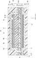
実施形態1に係るフレキシブルプリント配線板を説明する。まず、フレキシブルプリント配線板の構成を説明する。図1は、実施形態1に係るフレキシブルプリント配線板を例示した断面図である。図1に示すように、フレキシブルプリント配線板1は、積層配線板100、シールドフィルム部201、シールドフィルム部202、カバー層301、カバー層302を備えている。フレキシブルプリント配線板1は、フィルム状の部材、厚さが薄い部材、可撓性の部材等を含むため、フレキシブル性を有する。フレキシブルプリント配線板1は、平らにした状態で一方向に延びている。
(Embodiment 1)
A flexible printed wiring board according to Embodiment 1 will be described. First, the configuration of the flexible printed wiring board will be described. FIG. 1 is a cross-sectional view illustrating a flexible printed wiring board according to the first embodiment. As shown in FIG. 1, the flexible printed
ここで、フレキシブルプリント配線板1の説明の便宜上、XYZ直交座標系を導入する。フレキシブルプリント配線板1を平らにした状態で、フレキシブルプリント配線板1が延びる方向をX軸方向とする。フレキシブルプリント配線板1の上面に直交する方向をZ軸方向とする。よって、フレキシブルプリント配線板1の厚さ方向はZ軸方向である。Y軸方向には、フレキシブルプリント配線板1の両端面が向いている。
Here, for convenience of explanation of the flexible printed
積層配線板100は、一方向、すなわち、X軸方向に延びている。積層配線板100は、例えば、フレキシブル性を有する配線板である。積層配線板100は、導電層11、導電層12、絶縁層21、絶縁層22、絶縁層23、信号回路30及びグランド回路40を含んでいる。積層配線板100は、下方から、導電層11、絶縁層21、絶縁層22、絶縁層23及び導電層12の順で積層されている。絶縁層21と絶縁層22との間に、信号回路30及びグランド回路40が設けられている。なお、積層配線板100において、各層の間に他の導電層または絶縁層が挿入されてもよい。積層配線板100の上面102に平行な面内における一方向に直交する他方向、すなわち、Y軸方向において、両端面は対向している。
The laminated
導電層11は、例えば、積層配線板100の下面101に渡って形成されている。絶縁層21は、導電層11上に設けられている。信号回路30は、絶縁層21上に設けられている。信号回路30は、絶縁層21上において、X軸方向に延びた部分を有している。信号回路30は、複数本設けられてもよい。信号回路30は、例えば、信号回路31及び信号回路32を有してもよい。例えば、信号回路31は、信号回路32の−Y軸方向側に配置されている。
The
グランド回路40は、絶縁層21上に設けられている。グランド回路40は、絶縁層21上において、X軸方向に延びた部分を有している。グランド回路40は、信号回路30と距離を空けて設けられている。グランド回路40は、信号回路30に沿ってX軸方向に延びた部分を有している。グランド回路40は、複数本設けられてもよい。グランド回路40は、例えば、グランド回路41及びグランド回路42を有してもよい。例えば、グランド回路41は、信号回路31の−Y軸方向側に配置されている。グランド回路42は、信号回路32の+Y軸方向側に配置されている。グランド回路41及びグランド回路42は、信号回路31及び32を+Y軸方向側及び−Y軸方向側の両側から挟むように設けられている。よって、信号回路30は、グランド回路41とグランド回路42との間に配置されている。
The
絶縁層22は、絶縁層21、信号回路30及びグランド回路40上に設けられている。絶縁層22は、信号回路30及びグランド回路40を上方から覆うように、絶縁層21上に設けられている。絶縁層23は、絶縁層22上に設けられている。導電層12は、絶縁層23上に設けられている。
The insulating
積層配線板100は、例えば、両面フレキシブル銅張積層板(以下、両面FCCLという。)及び片面フレキシブル銅張積層板(以下、片面FCCLという。)を用いて形成されてもよい。両面FCCLは、フィルム状の絶縁性基材層の両面に銅箔が形成されたものでる。片面FCCLは、フィルム状の絶縁性基材層の片面に銅箔が形成されたものでる。
The
両面FCCLの一方の面の銅箔は、導電層11として用いられ、絶縁性基材層は、絶縁層21として用いられる。他方の面の銅箔は、パターニングされて、信号回路30及びグランド回路40として用いられる。また、片面FCCLの一方の面の銅箔は、導電層12として用いられ、絶縁性基材層は、絶縁層23として用いられる。両面FCCL及び片面FCCLを用いる場合には、以下のようにして、積層配線板100を形成する。すなわち、両面FCCLにおける他方の面をパターニングすることにより、信号回路30及びグランド回路40を形成する。次に、両面FCCLのパターニングされた面に、片面FCCLの絶縁性基材層側を接着する。これにより、積層配線板100が形成される。接着の際に用いられる絶縁性接着剤は、絶縁層22となる。
The copper foil on one side of the double-sided FCCL is used as the
両面及び片面FCCLの絶縁性基材層は、ポリエステル、ポリカーボネート、ポリイミド、ポリフェニレンサルファイド、液晶ポリマーが好ましく、液晶ポリマーおよびポリイミドがより好ましい。これらの中でも高周波の信号を伝送するフレキシブルプリント配線板の用途を考慮すると、比誘電率および誘電正接が低い液晶ポリマーがさらに好ましい。これらのような絶縁性基材を備えることで、フレキシブルプリント配線板1は、高い耐熱性が得られる。
The double-sided and single-sided FCCL insulating substrate layers are preferably polyester, polycarbonate, polyimide, polyphenylene sulfide, and liquid crystal polymer, and more preferably liquid crystal polymer and polyimide. Among these, a liquid crystal polymer having a low relative dielectric constant and dielectric loss tangent is more preferable in consideration of the use of a flexible printed wiring board that transmits a high-frequency signal. By providing such an insulating base material, the flexible printed
信号回路30は、フレキシブルプリント配線板1を介して接続された電子部材に電気信号を送る。グランド回路40は、アースを取るための接地電位に設定される。導電層11、導電層12、信号回路30及びグランド回路40に用いられる材料は、導電性であれば、銅箔に限らない。また、積層配線板100は、両面FCCL及び片面FCCLを用いて形成されたものに限らない。例えば、導電層11、絶縁層21、信号回路30及びグランド回路40、絶縁層22、絶縁層23、並びに、導電層12を順に積層することにより形成してもよい。
The
導電層11、導電層12、信号回路30及びグランド回路40の厚さは、例えば、18[μm]である。絶縁層21及び絶縁層23の厚さは、例えば、50[μm]である。絶縁層22の厚さは、例えば、35[μm]である。なお、積層配線板100に含まれた各層の厚さは、積層配線板100がフレキシブルであれば、上述の厚さに限らず、1〜200[μm]程度でもよい。
The thicknesses of the
絶縁性のカバー層301は、積層配線板100の下方に設けられている。絶縁性のカバー層302は、積層配線板100の上方に設けられている。カバー層301及び302は、積層配線板100を覆い、外部環境から保護する絶縁材料である。導電層11及び12は、積層配線板100の下面101及び上面102に渡って露出されているので、カバー層301及び302は、導電層11及び12を覆う。カバー層301及び302は、例えば、カバーレイ61及び絶縁性接着剤層62を含んでいる。カバーレイ61は、例えば、材料として、ポリイミド等の樹脂を含んでいる。絶縁性接着剤層62は、例えば、絶縁性の接着剤である。なお、カバー層301及び302は、カバーレイ61及び絶縁性接着剤層62を含む構成に限らず、熱硬化型もしくは紫外線硬化型のソルダーレジスト、感光性カバーレイフィルム、微細加工に適した感光性カバーレイフィルム等でもよく、熱硬化性接着剤等でもよい。カバー層301及び302の厚さは、例えば、10〜100[μm]であり、好ましくは、例えば、60[μm]である。カバーレイ61の厚さは、例えば、25[μm]であり、絶縁性接着剤層62の厚さは、例えば、35[μm]である。
The insulating
カバー層301及び302は、絶縁性接着剤層62側を積層配線板100に接着させている。カバー層301及び302には、貫通孔63が形成されている。貫通孔63は、カバーレイ61及び絶縁性接着剤層62を貫通している。貫通孔63の内部には、アースビア64が形成されている。よって、アースビア64は、カバー層301及び302を貫通する。
The cover layers 301 and 302 have the insulating
シールドフィルム部201及び202は、絶縁性の絶縁被覆層52及び導電性のシールド層51を含んでいる。シールドフィルム部201及び202は、絶縁被覆層52の片面に、シールド層51が形成されたものである。シールドフィルム部201及び202をまとめて、シールドフィルム200ともいう。よって、シールドフィルム200は、積層配線板100の下面101を覆うシールドフィルム部201と、上面102を覆うシールドフィルム部202と、を含んでいる。シールドフィルム200は、積層配線板100をシールドする。
The
シールド層51は、例えば、シールドフィルム200の導電性接着剤が硬化したものである。したがって、シールドフィルム200は、フレキシブルプリント配線板1においては、シールド層51と絶縁被覆層52とを含み、フレキシブルプリント配線板1の部材となる前の単体では、導電性接着剤層と絶縁被覆層52とを含んでいる。なお、シールドフィルム200のシールド層51は、導電性を有していれば、導電性接着剤が硬化したものに限らない。
For example, the
また、図12に示すように、シールドフィルム200は、絶縁被覆層52と、シールド層51との間に形成された金属層53を含んでもよい。すなわち、シールドフィルム200は、フレキシブルプリント配線板1においては、導電性接着剤が硬化したシールド層51と、絶縁被覆層52と、両者の間の金属層53と、から構成され、フレキシブルプリント配線板1の部材となる前の単体では、導電性接着剤層、金属層53及び絶縁被覆層52が積層されたものでもよい。金属層53は、例えば、銅箔である。
As shown in FIG. 12, the
ここで、シールドフィルム200における導電性接着剤層及び絶縁被覆層52を説明する。
Here, the conductive adhesive layer and the insulating
<<導電性接着剤層>>
導電性接着剤層は、等方導電性接着剤層または異方導電性接着剤層から適宜選択できる。等方導電性接着剤層は、シールドフィルム200を水平に置いた状態で、上下方向および水平方向に導電性を有する。また、異方導電性接着剤層は、シールドフィルム200を水平に置いた状態で、上下方向のみに導電性を有する。導電性接着剤層は、等方導電性あるいは異方導電性のいずれでもよく、等方導電性の場合、アースビア64での接続信頼性が向上するため好ましい。また、フレキシブルプリント配線板1の端面103及び104からのノイズ漏洩の低減にも効果的である。導電性接着剤層は、導電性接着剤を使用して形成できる。導電性接着剤は、熱硬化性樹脂、硬化剤、および導電性微粒子を含む従来公知のものを任意に用いることが可能である。以下で、熱硬化性樹脂、硬化剤、及び、導電性微粒子を説明する。
<< Conductive adhesive layer >>
The conductive adhesive layer can be appropriately selected from an isotropic conductive adhesive layer or an anisotropic conductive adhesive layer. The isotropic conductive adhesive layer has conductivity in the vertical direction and the horizontal direction with the
<熱硬化性樹脂>
熱硬化性樹脂は、硬化剤と反応可能な官能基を複数有する樹脂である。官能基は、例えば、水酸基、フェノール性水酸基、メトキシメチル基、カルボキシル基、アミノ基、エポキシ基、オキセタニル基、オキサゾリン基、オキサジン基、アジリジン基、チオール基、イソシアネート基、ブロック化イソシアネート基、ブロック化カルボキシル基、シラノール基等が挙げられる。熱硬化性樹脂は、例えば、アクリル樹脂、マレイン酸樹脂、ポリブタジエン系樹脂、ポリエステル樹脂、ポリウレタン樹脂、ポリウレタンウレア樹脂、エポキシ樹脂、オキセタン樹脂、フェノキシ樹脂、ポリイミド樹脂、ポリアミド樹脂、ポリアミドイミド樹脂、フェノール系樹脂、アルキド樹脂、アミノ樹脂、ポリ乳酸樹脂、オキサゾリン樹脂、ベンゾオキサジン樹脂、シリコーン樹脂、フッ素樹脂等の公知の樹脂が挙げられる。
<Thermosetting resin>
A thermosetting resin is a resin having a plurality of functional groups capable of reacting with a curing agent. Functional groups include, for example, hydroxyl group, phenolic hydroxyl group, methoxymethyl group, carboxyl group, amino group, epoxy group, oxetanyl group, oxazoline group, oxazine group, aziridine group, thiol group, isocyanate group, blocked isocyanate group, blocked A carboxyl group, a silanol group, etc. are mentioned. Thermosetting resins include, for example, acrylic resins, maleic resins, polybutadiene resins, polyester resins, polyurethane resins, polyurethane urea resins, epoxy resins, oxetane resins, phenoxy resins, polyimide resins, polyamide resins, polyamideimide resins, phenolic resins. Known resins such as resins, alkyd resins, amino resins, polylactic acid resins, oxazoline resins, benzoxazine resins, silicone resins, and fluorine resins can be used.
熱硬化性樹脂は、単独または2種類以上併用できる。これらの中でも屈曲性の点から、ポリウレタン樹脂、ポリウレタンウレア樹脂、エポキシ樹脂、フェノキシ樹脂、ポリイミド樹脂、ポリアミド樹脂、ポリアミドイミド樹脂が好ましい。熱硬化性樹脂の酸価は、1〜50mgKOH/gが好ましく、3〜30mgKOH/gがより好ましい。熱硬化性樹脂の重量平均分子量は、20000〜100000が好ましい。熱硬化性樹脂は、導電性接着剤層の固形分中の含有量が、5〜99重量%配合することが好ましく、7〜80重量%がより好ましく、10〜60重量%がさらに好ましい。 Thermosetting resins can be used alone or in combination of two or more. Among these, polyurethane resin, polyurethane urea resin, epoxy resin, phenoxy resin, polyimide resin, polyamide resin, and polyamideimide resin are preferable from the viewpoint of flexibility. 1-50 mgKOH / g is preferable and, as for the acid value of a thermosetting resin, 3-30 mgKOH / g is more preferable. The weight average molecular weight of the thermosetting resin is preferably 20,000 to 100,000. The content of the thermosetting resin in the solid content of the conductive adhesive layer is preferably 5 to 99% by weight, more preferably 7 to 80% by weight, and still more preferably 10 to 60% by weight.
<硬化剤>
硬化剤は、熱硬化性樹脂の官能基と反応可能な官能基を複数有している。硬化剤は、例えば、エポキシ化合物、酸無水物基含有化合物、イソシアネート化合物、アジリジン化合物、アミン化合物、フェノール化合物、有機金属化合物等の公知の化合物が挙げられる。硬化剤は、単独または2種類以上併用できる。硬化剤は、熱硬化性樹脂100重量部に対して各種1〜50重量部含むことが好ましく、3〜30重量部がより好ましく、3〜20重量部がさらに好ましい。
<Curing agent>
The curing agent has a plurality of functional groups that can react with the functional groups of the thermosetting resin. Examples of the curing agent include known compounds such as an epoxy compound, an acid anhydride group-containing compound, an isocyanate compound, an aziridine compound, an amine compound, a phenol compound, and an organometallic compound. A hardening | curing agent can be used individually or in combination with 2 or more types. It is preferable that 1-50 weight part of various hardening | curing agents are included with respect to 100 weight part of thermosetting resins, 3-30 weight part is more preferable, and 3-20 weight part is further more preferable.
<導電性微粒子>
導電性微粒子は、導電性接着剤層に導電性を付与する機能を有する。導電性微粒子は、素材としては、例えば金、白金、銀、銅およびニッケル等の導電性金属およびその合金、ならびに導電性ポリマーの微粒子が好ましく、価格と導電性の面からは、銀または銅がより好ましい。
<Conductive fine particles>
The conductive fine particles have a function of imparting conductivity to the conductive adhesive layer. The conductive fine particles are preferably, for example, conductive metals such as gold, platinum, silver, copper and nickel, and alloys thereof, and conductive polymer fine particles. From the viewpoint of price and conductivity, silver or copper is preferable. More preferred.
また単一素材の微粒子ではなく金属や樹脂を核体とし、核体の表面を被覆した被覆層を有する複合微粒子もコストダウンの観点から好ましい。ここで核体は、価格が安いニッケル、シリカ、銅およびその合金、ならびに樹脂から適宜選択することが好ましい。被覆層は、導電性金属または導電性ポリマーが好ましい。導電性金属は、例えば、金、白金、銀、ニッケル、マンガン、およびインジウム等、ならびにその合金が挙げられる。また導電性ポリマーは、ポリアニリン、ポリアセチレン等が挙げられる。これらの中でも価格と導電性の面から銀または銅が好ましい。 In addition, composite fine particles having a coating layer in which a metal or a resin is used as a core and the surface of the core is covered, are preferable from the viewpoint of cost reduction. Here, the core is preferably selected appropriately from inexpensive nickel, silica, copper and alloys thereof, and resins. The coating layer is preferably a conductive metal or a conductive polymer. Examples of the conductive metal include gold, platinum, silver, nickel, manganese, indium, and alloys thereof. Examples of the conductive polymer include polyaniline and polyacetylene. Among these, silver or copper is preferable from the viewpoints of price and conductivity.
導電性微粒子の形状は、所望の導電性が得られればよく形状は限定されない。具体的には、例えば、球状、フレーク状、葉状、樹枝状、プレート状、針状、棒状、ブドウ状が好ましい。また、これらの異なる形状の導電性微粒子を2種類混合しても良い。
導電性微粒子は、単独または2種類以上併用できる。
The shape of the conductive fine particles is not limited as long as desired conductivity is obtained. Specifically, for example, a spherical shape, a flake shape, a leaf shape, a dendritic shape, a plate shape, a needle shape, a rod shape, and a grape shape are preferable. Moreover, you may mix two types of electroconductive fine particles of these different shapes.
The conductive fine particles can be used alone or in combination of two or more.
導電性微粒子の平均粒子径は、D50平均粒子径であり、導電性を充分に確保する観点から、2μm以上が好ましく、5μm以上がより好ましく、7μm以上とすることが更に好ましい。一方、導電性接着剤層の薄さと両立させる観点からは、30μm以下が好ましく、20μm以下がより好ましく、15μm以下とすることが更に好ましい。D50平均粒子径は、レーザー回折・散乱法粒度分布測定装置等により求めることができる。 The average particle diameter of the conductive fine particles is a D50 average particle diameter, and is preferably 2 μm or more, more preferably 5 μm or more, and further preferably 7 μm or more from the viewpoint of sufficiently ensuring conductivity. On the other hand, from the viewpoint of making the conductive adhesive layer thin, 30 μm or less is preferable, 20 μm or less is more preferable, and 15 μm or less is even more preferable. The D50 average particle diameter can be determined by a laser diffraction / scattering particle size distribution measuring apparatus or the like.
導電性微粒子は、導電性接着剤層の固形分中の含有量が、1〜95重量%配合することが好ましく、20〜93重量%がより好ましく、40〜90重量%がさらに好ましい。100重量部に対して、10〜700重量部を配合することが好ましく、20〜500重量部がより好ましい。含有量が20〜500重量部であることにより、電磁波シールド性がより良好なシールドフィルム200とすることができる。
The content of the conductive fine particles in the solid content of the conductive adhesive layer is preferably 1 to 95% by weight, more preferably 20 to 93% by weight, and still more preferably 40 to 90% by weight. It is preferable to mix | blend 10-700 weight part with respect to 100 weight part, and 20-500 weight part is more preferable. When content is 20-500 weight part, it can be set as the
導電性接着剤は、他に任意成分としてシランカップリング剤、防錆剤、還元剤、酸化防止剤、顔料、染料、粘着付与樹脂、可塑剤、紫外線吸収剤、消泡剤、レベリング調整剤、充填剤、難燃剤などを配合できる。 Conductive adhesives include silane coupling agents, rust inhibitors, reducing agents, antioxidants, pigments, dyes, tackifying resins, plasticizers, UV absorbers, antifoaming agents, leveling regulators as optional components. Fillers and flame retardants can be blended.
導電性接着剤は、これまで説明した材料を混合し攪拌して得ることができる。攪拌は、例えばディスパーマット、ホモジナイザー等に公知の攪拌装置を使用できる。 The conductive adhesive can be obtained by mixing and stirring the materials described so far. For the stirring, for example, a known stirring device can be used for a disperse mat, a homogenizer or the like.
導電性接着剤層の作製は、公知の方法を使用できる。例えば、導電性接着剤を剥離性シート上に塗工して乾燥することで導電層を形成する方法、または、Tダイのような押出成形機を使用して導電性接着剤をシート状に押し出すことで形成することもできる。 A known method can be used for producing the conductive adhesive layer. For example, a method of forming a conductive layer by applying a conductive adhesive on a peelable sheet and drying, or extruding the conductive adhesive into a sheet using an extruder such as a T-die It can also be formed.
塗工方法は、例えば、グラビアコート方式、キスコート方式、ダイコート方式、リップコート方式、コンマコート方式、ブレード方式、ロールコート方式、ナイフコート方式、スプレーコート方式、バーコート方式、スピンコート方式、ディップコート方式等の公知の塗工方法を使用できる。塗工に際して、乾燥工程を行うことが好ましい。乾燥工程は、例えば、熱風乾燥機、赤外線ヒーター等の公知の乾燥装置を使用できる。 Coating methods include, for example, gravure coating method, kiss coating method, die coating method, lip coating method, comma coating method, blade method, roll coating method, knife coating method, spray coating method, bar coating method, spin coating method, dip coating. A known coating method such as a method can be used. In coating, it is preferable to perform a drying step. In the drying step, for example, a known drying device such as a hot air dryer or an infrared heater can be used.
導電性接着剤層の厚みは、2〜100μmが好ましく、4〜50μmがより好ましく、6〜30μmがさらに好ましい。厚みが2〜100μmの範囲にあることで電磁波シールド性と屈曲性とのバランスを取り易くなる。 2-100 micrometers is preferable, as for the thickness of a conductive adhesive layer, 4-50 micrometers is more preferable, and 6-30 micrometers is further more preferable. When the thickness is in the range of 2 to 100 μm, it becomes easy to balance the electromagnetic shielding properties and the flexibility.
<<絶縁被覆層>>
絶縁被覆層は、従来公知の絶縁性樹脂組成物を使用して形成できる。絶縁性樹脂組成物は、導電性接着剤で説明した熱硬化性樹脂および硬化剤を必要に応じて任意成分を含むことができる。なお、絶縁層および導電性接着剤層に使用する熱硬化性樹脂、硬化剤は、同一、または異なっていてもよい。絶縁性樹脂組成物は、導電性接着剤と同様の方法で得ることが出来る。また、絶縁層は、ポリエステル、ポリカーボネート、ポリイミド、ポリフェニレンサルファイド等の絶縁性樹脂を成形したフィルムを使用することもできる。絶縁層の厚みは、通常2〜20μm程度である。
<< Insulation coating layer >>
The insulating coating layer can be formed using a conventionally known insulating resin composition. The insulating resin composition can contain an optional component as necessary for the thermosetting resin and the curing agent described in the conductive adhesive. The thermosetting resin and the curing agent used for the insulating layer and the conductive adhesive layer may be the same or different. The insulating resin composition can be obtained by the same method as that for the conductive adhesive. The insulating layer may be a film formed of an insulating resin such as polyester, polycarbonate, polyimide, polyphenylene sulfide or the like. The thickness of the insulating layer is usually about 2 to 20 μm.
シールドフィルム部201は、積層配線板100の下面101をシールド層51側で覆う。したがって、シールド層51側の面が積層配線板100側の下面101に向いている。シールドフィルム部201は、積層配線板100を覆い、カバー層301に接触している。よって、カバー層301は、積層配線板100の下面101と、下面101を覆うシールドフィルム部201との間に設けられている。シールドフィルム部201は、積層配線板100の下面101をシールド層51側で覆うとともに、積層配線板100の、Y軸方向の両端面の少なくとも一部を、シールド層51側で覆う。例えば、シールドフィルム部201は、積層配線板100の導電層11、絶縁層21及び絶縁層22の両端面を覆う。したがって、シールドフィルム部201は、導電層11の両端面と接触する。また、シールドフィルム部201は、カバー層301の両端面を覆う。
The
シールドフィルム部202は、積層配線板100の上面102をシールド層51側で覆う。したがって、シールド層51側の面が積層配線板100側の上面102に向いている。シールドフィルム部202は、積層配線板100を覆い、カバー層302に接触している。よって、カバー層302は、積層配線板100の上面102と、上面102を覆うシールドフィルム部202との間に設けられている。シールドフィルム部202は、積層配線板100の上面102をシールド層51側で覆うとともに、積層配線板100の、Y軸方向の両端面の少なくとも一部を、シールド層51側で覆う。例えば、シールドフィルム部202は、積層配線板100の導電層12、絶縁層23及び絶縁層22の両端面を覆う。したがって、シールドフィルム部202は、導電層12の両端面と接触する。また、シールドフィルム部202は、カバー層302の両端面を覆う。
The
積層配線板100の両端面、すなわち、端面103及び104は、導電層11から導電層12に渡って、シールド層51に覆われている。積層配線板100の両端面は、全面に渡って、シールドフィルム部201及びシールドフィルム部202のシールド層51に覆われている。
Both end surfaces of the
なお、シールドフィルム部201及び202が、積層配線板100のY軸方向における両端面を覆う境界は、絶縁層22の両端面に限らない。例えば、シールドフィルム部201は、カバー層301及び導電層11の両端面を覆い、シールドフィルム部202は、カバー層302、導電層12、絶縁層23、絶縁層22、及び、絶縁層21の両端面を覆うというように、シールドフィルム部201及び202の両端面における境界は、両端面のどこでもよい。
The boundary where
シールドフィルム部201及び202のシールド層51は、信号回路30に沿ってX軸方向に延びるように両端面を覆ってもよい。また、シールド層51は、信号回路30に沿って両端面の全面を覆ってもよい。シールドフィルム部201及び202のシールド層51は、積層配線板100の両端面から外側のY軸方向に延びる部分を有してもよい。シールド層51は、−Y軸方向側の端面103から−Y軸方向に延びる部分と、+Y軸方向側の端面104から+Y軸方向に延びる部分と、を有してもよい。
The shield layers 51 of the
カバー層301及び302を貫通するアースビア64は、シールド層51に含まれた導電性材料と同じ材料を含んでもよい。例えば、シールド層51の一部が、貫通孔63の内部に充填されることにより、アースビア64は、シールド層51に含まれた導電性材料と同じ材料を含んでもよい。シールド層51は、アースビア64を介して導電層11及び導電層12と接続されている。カバー層301及び302を貫通するアースビア64は、グランド回路40の直上に配置されてもよい。
The ground via 64 that penetrates the cover layers 301 and 302 may include the same material as the conductive material included in the
次に、実施形態1に係るフレキシブルプリント配線板1の製造方法を説明する。図2は、実施形態1に係るフレキシブルプリント配線板1の製造方法を例示したフローチャート図である。
Next, a method for manufacturing the flexible printed
図2のステップS11に示すように、まず、積層配線板100を準備する。積層配線板100は、導電層11と、導電層11上に設けられた絶縁層21と、絶縁層21上に設けられ、X軸方向に延びた部分を有する信号回路30と、絶縁層21及び信号回路30上に設けられた絶縁層22及び23と、絶縁層23上に設けられた導電層12と、を含んでいる。
As shown in step S11 of FIG. 2, first, the
次に、ステップS12に示すように、シールドフィルム200を準備する。具体的には、絶縁性の絶縁被覆層52の片面に導電性のシールド層51が形成されたシールドフィルム部201及び202を準備する。なお、ステップS11とステップS12は順序が逆になってもよいし、同時でもよい。
Next, as shown in step S12, the
次に、ステップS13に示すように、シールドフィルム200で積層配線板100を覆う。具体的には、積層配線板100の下面101を、絶縁性のカバー層301を介して、シールドフィルム部201のシールド層51側で覆い、積層配線板100の上面102を、絶縁性のカバー層302を介して、シールドフィルム部202のシールド層51側で覆う。また、それとともに、積層配線板100のY軸方向の両端面の少なくとも一部を、シールドフィルム部201及び202のシールド層51側で覆う。なお、カバー層302には、貫通孔63が設けられている。また、カバー層301にも、貫通孔63が設けられていることが望ましい。
Next, as shown in step S <b> 13, the
次に、ステップS14に示すように、プレスする。例えば、熱を加えて熱プレスする。具体的には、積層配線板100及び積層配線板100を覆うシールドフィルム201及び202を上下方向にプレスする。例えば、熱プレスは、温度150〜190[℃]程度、圧力1〜3[MPa]程度、時間1〜60[min]程度が好ましい。これにより、積層配線板100、カバー層301及び302、並びに、シールドフィルム部201及び202を圧着させる。この際に、貫通孔63にシールド層51の一部を充填させる。このようにして、フレキシブルプリント配線板1を製造することができる。
Next, as shown in step S14, pressing is performed. For example, heat pressing is performed by applying heat. Specifically, the
次に、本実施形態の効果を説明する前に、比較例を説明する。その後、比較例と対比させて、本実施形態の効果を説明する。図3は、比較例に係るフレキシブルプリント配線板1110を例示した断面図である。図3に示すように、フレキシブルプリント配線板1110において、積層配線板100の両端面は、シールドフィルム200で覆われていない。よって、積層配線板100の両端面からの放射ノイズ1012の漏れを抑制することができない。
Next, a comparative example will be described before describing the effects of the present embodiment. Then, the effect of this embodiment is demonstrated compared with a comparative example. FIG. 3 is a cross-sectional view illustrating a flexible printed
図4は、実施形態1に係るフレキシブルプリント配線板1の要部を例示した断面図である。図4に示すように、本実施形態のフレキシブルプリント配線板1は、積層配線板100の上面102及び下面101だけでなく、積層配線板100の両端面、すなわち、−Y軸方向側の端面103及び+Y軸方向側の端面104をシールド層51で覆っている。よって、積層配線板100の両端面からの放射ノイズの漏れを抑制することができる。
FIG. 4 is a cross-sectional view illustrating the main part of the flexible printed
また、高周波信号が流れる信号回路30を、グランド回路40で挟むように配置させている。これにより、放射ノイズのシールド性を向上させることができる。
Further, the
信号回路30の下方には、導電層11及びシールド層51が配置され、信号回路30の上方には、導電層12及びシールド層51が配置されている。このように、2重にシールドされているので、シールド性を向上させることができる。
The
信号回路30の下方において、導電層11とシールド層51とがアースビア64によって接続されている。これにより、導電層11とシールド層51とを確実に同電位とすることができる。また、信号回路30の上方において、導電層12とシールド層51とがアースビア64によって接続されている。これにより、導電層12とシールド層51とを確実に同電位とすることができる。よって、放射ノイズのシールド性を向上させることができる。
Below the
アースビア64は、導電層11及び12まで貫通し、グランド回路40まで貫通していない。アースビア64は、カバー層301及び302に形成された貫通孔63に形成される。よって、アースビア64を導電層11及び12に貫通させなくてもよいので、製造を容易にし、コストを低減させることができる。また、導電層11及び導電層12が、導電性接着剤層から形成されておらず、FCCLの銅箔等の金属層から形成されている場合には、導電性接着剤層から形成されたものに比べて、シールド性を向上させることができる。このことは、図12に示すように、シールドフィルム200において、シールド層51と絶縁被覆層52との間に金属層53が配置されている場合にもあてはまる。すなわち、シールドフィルム200の金属層53は、シールド性を向上させることができる。
The earth via 64 penetrates to the
また、導電層11及び12が金属層であることは、シールド性の効果の他、高周波領域での伝送特性に優れているという効果をもたらす。これにより、信号の高周波化、しいては、データ処理の高速化に対応させることができる。このようなメリット、すなわち、シールド性が高いこと、及び、伝送特性に優れることにより、フレキシブルプリント配線板1(FPC)を伝搬する信号を、外部ノイズや伝搬時の信号劣化から守ることができ、従来性能的に使用できなかった箇所にも使用することができる。
Further, the fact that the
さらに、シールドフィルム200のシールド層51は、導電性接着剤層から形成されているので、積層配線板100への密着性を向上させることができる。
Furthermore, since the
アースビア64は、グランド回路40の直上または直下に形成されている。よって、導電層11と導電層12との間の空間電位、導電層11とシールド層51との間の空間電位、及び、導電層12とシールド層51との間の空間電位を同等にすることができ、シールド性を向上させることができる。
The earth via 64 is formed immediately above or directly below the
シールドフィルム部201及びシールドフィルム部202のシールド層51は、積層配線板100の両端面から外側のY軸方向に延びる部分を有している。これにより、積層配線板100の両端面からの放射ノイズの漏れを抑制することができる。
The
(実施形態2)
次に、実施形態2に係るフレキシブルプリント配線板を説明する。図5は、実施形態2に係るフレキシブルプリント配線板を例示した断面図である。図5に示すように、フレキシブルプリント配線板2は、フレキシブルプリント配線板1と比べて、シールドフィルム200の構成が異なっている。すなわち、フレキシブルプリント配線板2は、実施形態1のシールドフィルム部201及び202の代わりに、1枚のシールドフィルム203を備えている。積層配線板100、カバー層301及びカバー層302の構成は、実施形態1と同様であるので説明を省略する。
(Embodiment 2)
Next, a flexible printed wiring board according to the second embodiment will be described. FIG. 5 is a cross-sectional view illustrating a flexible printed wiring board according to the second embodiment. As shown in FIG. 5, the flexible printed
フレキシブルプリント配線板2では、1枚のシールドフィルム203によって、積層配線板100を覆っている。シールドフィルム203は、例えば、積層配線板100の下面101の中央部分から覆い始めている。覆い始めの部分を始点部203aという。シールドフィルム203は、始点部203aから、積層配線板100の端面103、上面102、端面104を順に覆い、積層配線板100の下面101の中央部分で、始点部203aに重なっている。始点部203aに重なって巻き終えた部分を終点部203bという。
In the flexible printed
積層配線板100の下面101の中央部分において、始点部203aに、終点部203bが重なっている。よって、重なった部分では、始点部203aの絶縁被覆層52上に、終点部203bのシールド層51が重なっている。このように、フレキシブルプリント配線板2において、シールドフィルム203は、重なることにより、シールド層51とシールド層51との間に絶縁被覆層52が挟まれた部分を有している。
In the central portion of the
また、シールドフィルム203のシールド層51は、積層配線板100のY軸方向の両端面から外側のY軸方向に延びる部分を有している。シールド層51は、−Y軸方向側の端面103から−Y軸方向に延びる部分と、+Y軸方向側の端面104から+Y軸方向に延びる部分と、を有している。例えば、積層配線板100及び積層配線板100を覆うシールドフィルム203を上下方向に熱プレスする際に、シールド層51を、積層配線板100のY軸方向の両端面から外側のY軸方向に延びるようにすることができる。
Further, the
次に、実施形態2に係るフレキシブルプリント配線板2の製造方法を説明する。本実施形態のフレキシブルプリント配線板2の製造方法は、実施形態1の製造方法に比べて、シールドフィルム200を準備する工程と、シールドフィルム200で積層配線板100を覆う工程とが異なっている。
Next, a method for manufacturing the flexible printed
実施形態2では、シールドフィルム200を準備する工程において、シールドフィルム部201及び202を準備する代わりに、1枚のシールドフィルム203を準備する。シールドフィルム203は、絶縁性の絶縁被覆層52の片面に導電性のシールド層51が形成されたものである。
In the second embodiment, in the step of preparing the
また、シールドフィルム203で積層配線板100を覆う工程において、シールドフィルム203を、積層配線板100の下面101から、−Y軸方向側の端面103、上面102、+Y軸方向側の端面104の順に、積層配線板100の周囲を巻くように覆う。そして、シールドフィルム203を重ねることにより、シールド層51とシールド層51との間に絶縁被覆層52が挟まれた部分を有するようにする。このようにして、フレキシブルプリント配線板2を製造することができる。
Further, in the step of covering the
本実施形態のフレキシブルプリント配線板2によれば、シールドフィルム203は、積層配線板100の周囲を巻くように覆っている。よって、放射ノイズの漏れを抑制することができる。また、シールドフィルム203の接合部分は、始点部203aと終点部203bとが重なっている。これにより、接合部分からの放射ノイズの漏れを抑制することができる。これ以外の構成及び効果は、実施形態1の記載に含まれている。
According to the flexible printed
(実施形態3)
次に、実施形態3に係るフレキシブルプリント配線板3を説明する。図6は、実施形態3に係るフレキシブルプリント配線板を例示した断面図である。
(Embodiment 3)
Next, the flexible printed
図6に示すように、フレキシブルプリント配線板3は、導電層11からY軸方向に延びた延在導電層71と、絶縁層21からY軸方向に延びた延在絶縁層72と、を含む延在部70をさらに備えている。よって、延在部70は、積層配線板100の端面103から−Y軸方向側、及び、端面104から+Y軸方向側に設けられている。延在部70は、絶縁層22、絶縁層23及び導電層12の両端面よりもY軸方向の外側に延びている。また、両面FCCLを用いて導電層11及び絶縁層21を形成した際に、延在部70は、両面FCCLにおける信号回路30及びグランド回路40のパターニングで残存した導電層を含んでもよい。
As shown in FIG. 6, the flexible printed
複数の接続ビア74は、延在部70を貫通している。複数の接続ビア74は、延在部70において、X軸方向に沿って配列している。複数の接続ビア74は、シールド層51に含まれた材料と同じ材料を含んでもよい。また、複数の接続ビア74は、延在部70を貫通する貫通孔73の内面にメッキされた導電材料を含んでもよい。
The plurality of connection vias 74 penetrate through the extending
シールドフィルム200は、積層配線板100の下面101を覆うシールドフィルム部201と、上面102を覆うシールドフィルム部202と、を含んでいる。シールドフィルム部201は、カバー層301のY軸方向における両端面を覆っている。また、シールドフィルム部201は、延在部70の下面を覆っている。シールドフィルム部202は、絶縁層22、絶縁層23、導電層12、カバー層302のY軸方向における両端面を覆っている。また、シールドフィルム部202は、延在部70の上面を覆っている。したがって、シールドフィルム部201及びシールドフィルム部202のシールド層51は、積層配線板100のY軸方向における両端面から外側のY軸方向に延びる部分を有している。また、シールドフィルム部202は、延在部70を貫通する複数の接続ビア74を介して、シールドフィルム部201に接続されている。
The
次に、実施形態3に係るフレキシブルプリント配線板3の製造方法を説明する。本実施形態の製造方法は、実施形態1の製造方法に比べて、積層配線板100を準備する工程、シールドフィルム200で積層配線板100を覆う工程、及び、プレスする工程が異なっている。
Next, a method for manufacturing the flexible printed
実施形態3の製造方法では、積層配線板100を準備する工程において、導電層11からY軸方向に延びた延在導電層71と、絶縁層21からY軸方向に延びた延在絶縁層72と、を含む延在部70も準備する。延在部70には、複数の貫通孔73を形成する。複数の貫通孔73の内面を導電材料でメッキしてもよい。また、複数の貫通孔73の内部を導電ペーストで充填してもよい。
In the manufacturing method of the third embodiment, in the step of preparing the
シールドフィルム200で積層配線板100を覆う工程において、積層配線板100の下面101を、シールドフィルム部201のシールド層51側で覆う。それとともに、カバー層301のY軸方向における両端面、及び、延在部70の下面をシールドフィルム部201のシールド層51側で覆う。また、積層配線板100の上面102を、シールドフィルム部202のシールド層51側で覆う。それとともに、絶縁層22、絶縁層23、導電層12及びカバー層302のY軸方向における両端面、並びに、延在部70の上面をシールドフィルム部202のシールド層51側で覆う。
In the step of covering the
プレスする工程において、貫通孔73にシールド層51の一部を充填させる。なお、複数の貫通孔73の内面を導電材料でメッキした場合には、貫通孔73にシールド層51の一部を充填させなくてもよい。
In the pressing step, the through
本実施形態のフレキシブルプリント配線板3によれば、延在部70を有しているので、ハンドリングを容易にすることができる。また、シールドフィルム部201及び202の貼付を容易にすることができる。これ以外の構成及び効果は、実施形態1及び2の記載に含まれている。
According to the flexible printed
(変形例)
次に、実施形態3の変形例を説明する。図7は、実施形態3の変形例1に係るフレキシブルプリント配線板を例示した断面図であり、図8は、実施形態3の変形例2に係るフレキシブルプリント配線板を例示した断面図であり、図9は、実施形態3の変形例3に係るフレキシブルプリント配線板を例示した断面図である。
(Modification)
Next, a modification of the third embodiment will be described. 7 is a cross-sectional view illustrating a flexible printed wiring board according to
図7に示すように、フレキシブルプリント配線板3aにおいて、積層配線板100aは、導電層11、絶縁層21a、絶縁層22a、導電層12を含んでいる。絶縁層21aと絶縁層22aとの間に信号回路30及びグランド回路が設けられている。絶縁層21a及び絶縁層22aは、液晶ポリマーを材料に含んでいる。
As shown in FIG. 7, in the flexible printed
積層配線板100aは、例えば、両面FCCL及び片面FCCLを用いて形成されてもよい。両面FCCL及び片面FCCLの絶縁性基材層は、液晶ポリマーを材料に含んでいる。両面FCCLの一方の面の銅箔は、導電層11として用いられ、絶縁性基材層は、絶縁層21aとして用いられる。他方の面の銅箔は、パターニングされて、信号回路30及びグランド回路40として用いられる。また、片面FCCLの一方の面の銅箔は、導電層12として用いられ、絶縁性基材層は、絶縁層22aとして用いられる。両面FCCL及び片面FCCLを用いる場合には、以下のようにして積層配線板100aを形成する。すなわち、両面FCCLにおける他方の面をパターニングすることにより、信号回路30及びグランド回路40を形成する。次に、両面FCCLのパターニングされた面に、片面FCCLの絶縁性基材層側を接着する。これにより、積層配線板100aが形成される。
The
フレキシブルプリント配線板3aにおいて、延在部70は、延在導電層71及び延在絶縁層72aを含んでいる。延在導電層71及び延在絶縁層72aは、導電層11及び絶縁層21aと同じ材料を含んでいる。両面FCCLを用いて導電層11及び絶縁層21aを形成した際に、延在部70は、両面FCCLにおける信号回路30及びグランド回路40のパターニングで残存した導電層を含んでもよい。
In the flexible printed
積層配線板100aの下面101には、カバー層301の代わりに、レジスト層303が形成されている。また、積層配線板100aの上面102には、カバー層302の代わりに、レジスト層304が形成されている。レジスト層304には、貫通孔63が形成されている。貫通孔63の内部にアースビア64が形成されている。シールドフィルム部201及び202におけるシールド層51は、積層配線板100aを、レジスト層303及び304を介して覆っている。
Instead of the
図8に示すフレキシブルプリント配線板3bのように、レジスト層303及び304を省いてもよい。この場合には、シールドフィルム部201及び202におけるシールド層51は、積層配線板100aを、カバー層301及び302、または、レジスト層303及び304を介さずに直接覆っている。よって、導電層11及び12の表面は、導電性接着剤層から形成されたシールド層51で覆われているので、密着性を向上させることができる。また、導電層11及び12は、FCCLの銅箔等の金属層から形成されているので、前述したように、シールド性の効果及び伝送特性の効果を向上させることができる。これ以外の構成及び効果は、実施形態1〜3の記載に含まれている。
The resist layers 303 and 304 may be omitted as in the flexible printed
図9に示すフレキシブルプリント配線板3cのように、実施形態1に係るフレキシブルプリント配線板1のカバー層301及び302を省いてもよい。すなわち、フレキシブルプリント配線板3cは、X軸方向に延びた積層配線板100と、絶縁性の絶縁被覆層52の片面に導電性のシールド層51が形成されたシールドフィルム200であって、積層配線板100の上面102及び下面101を、シールド層51側で覆うとともに、積層配線板100のY軸方向の両端面の少なくとも一部を、シールド層51側で覆うシールドフィルム200と、を備えている。ここで、積層配線板100は、導電層11と、導電層11上に設けられた絶縁層21と、絶縁層21上に設けられ、X軸方向に延びた部分を有する信号回路30と、絶縁層21及び信号回路30上に設けられた絶縁層22と、絶縁層22上に設けられた導電層12と、を含んでいる。そして、シールド層51は導電層11及び導電層12と接続されている。
Like the flexible printed
このような構成でも、導電層11及び12の表面は、導電性接着剤層から形成されたシールド層51で覆われているので、密着性を向上させることができる。また、導電層11及び12は、FCCLの銅箔等の金属層から形成されているので、シールド性を向上させることができる。これ以外の構成及び効果は、実施形態1〜3の記載に含まれている。
Even in such a configuration, the surfaces of the
<実施例>
以下、実施例を示して本発明を更に具体的に説明するが、本発明はこれらによって限定されるものではない。まず、測定試料の作製方法を説明する。
<Example>
EXAMPLES Hereinafter, the present invention will be described more specifically with reference to examples, but the present invention is not limited thereto. First, a method for producing a measurement sample will be described.
[測定試料作製]
(実施例1)
積層配線板100を、両面FCCL及び片面FCCLを用いて作製する。両面FCCLは、厚さ50[μm]のポリイミドフィルムの両面に、厚さ12[μm]の圧延銅箔を積層させたものである。両面FCCLにおける一方の圧延銅箔に信号回路31及び32、並びに、グランド回路41及び42を形成する。信号回路31及び32、並びに、グランド回路41及び42のX軸方向の長さは、例えば、10[cm]である。グランド回路41及び42は、信号回路31及び32の両側の外側に、信号回路31及び32に平行に形成する。なお、回路の外観、公差の検査仕様は、JPCA規格(JPCA−DG02)とする。両面FCCLにおける他方の圧延銅箔は、導電層11となる。両面FCCLにおけるポリイミドフィルムは、絶縁層21となる。
[Measurement sample preparation]
(Example 1)
The
片面FCCLは、厚さ12.5[μm]のポリイミドフィルムの片面に、厚さ12[μm]の圧延銅箔を積層させたものである。片面FCCLにおける圧延銅箔は、導電層12である。片面FCCLにおけるポリイミドフィルムは、絶縁層23である。
Single-sided FCCL is obtained by laminating a rolled copper foil with a thickness of 12 [μm] on one side of a polyimide film with a thickness of 12.5 [μm]. The rolled copper foil in the single-sided FCCL is the
次に、片面FCCLのポリイミドフィルム側と、両面FCCLの回路形成面側とを、絶縁性接着剤を介して積層させる。そして、150[℃]の温度及び2.0[MPa]の圧力において、30[min]の条件で圧着する。絶縁接着剤は、厚さ35[μm]の絶縁層22となる。
Next, the polyimide film side of the single-sided FCCL and the circuit forming surface side of the double-sided FCCL are laminated via an insulating adhesive. Then, pressure bonding is performed under a condition of 30 [min] at a temperature of 150 [° C.] and a pressure of 2.0 [MPa]. The insulating adhesive becomes the insulating
そして、図示しない直径0.1[mm]のスルーホールを設け、次いで、無電解メッキ処理を行った後に、電解メッキ処理を行うことにより、導電層11及び12、並びに、グランド回路41及び42の導通を確保する。
Then, a through hole having a diameter of 0.1 [mm] (not shown) is provided, and then the electroless plating process is performed, and then the electroplating process is performed to thereby form the
さらに、導電層11及び12の外側面に、導電層11及び12を覆うように、カバー層301及び302を貼りつけ、150[℃]の温度及び2.0[MPa]の圧力において30[min]の条件で圧着する。カバー層301及び302は、厚さ12.5[μm]のポリイミドフィルムと、厚さ15[μm]の絶縁性接着剤層とで構成されている。カバー層301及び302には、貫通孔63が設けられている。その後、貫通孔63に露出した回路形成面、並びに、導電層11及び12にニッケルメッキ(不図示)を行い、次いで、金メッキ(不図示)処理を行う。そして、グランド回路41から−Y軸方向側に300[μm]、グランド回路42から+Y軸方向側に300[μm]の位置で裁断する。これにより、積層配線板100が形成される。
Further, cover layers 301 and 302 are attached to the outer surfaces of the
次に、図13に示すシールドフィルム200を、種類Aについて2枚用意し、積層配線板100のY軸方向の両端面103及び104を覆うように、其々のシールド層51を内側として、150[℃]の温度及び2.0[MPa]の圧力において、30[min]の条件で圧着する。そして、積層配線板100の両端面から+Y軸方向及び−Y軸方向側に1000[μm]の位置でシールドフィルム200を裁断する。これにより、シールドフィルム200のY軸方向の両端部にシールドフィルム200のみ重なった部分を1000[μm]の幅有するようにする。このようにして、フレキシブルプリント配線板1を得る。
Next, two types of
なお、図13に示すように、種類Aのシールドフィルム200において、絶縁被覆層52の厚さは、15[μm]であり、絶縁性接着剤層からなるシールド層51の厚さは、7[μm]である。絶縁性接着剤層の導電フィラー比率は、80[wt%]である。種類Aのシールドフィルム200は、金属層53を含んでいない。一方、種類Bのシールドフィルム200において、絶縁被覆層52の厚さは、15[μm]であり、シールド層51は、絶縁性接着剤層及び金属層53を含んでいる。絶縁性接着剤層の厚さは7[μm]である。絶縁性接着剤層の導電フィラー比率は、80[wt%]である。金属層53の厚さは、3[μm]である。金属層53は、例えば、電解銅箔を含んでいる。
As shown in FIG. 13, in the type
(実施例2〜9、比較例1及び2)
図14は、実施例1〜10の構成及び測定結果を例示した図である。図14に示すように、実施例1のフレキシブル配線板(FPC)の構成、シールドフィルムの種類、及び、シールドフィルム200被着後の裁断位置によって決まるシールドフィルムのみ重なった部分の幅を変更した以外は、実施例1と同様の試料作製を行うことで、実施例2〜9、比較例1、2のフレキシブルプリント配線板を得る。
(Examples 2 to 9, Comparative Examples 1 and 2)
FIG. 14 is a diagram illustrating the configuration and measurement results of Examples 1 to 10. As shown in FIG. 14, except for changing the width of the overlapping portion of only the shield film determined by the configuration of the flexible wiring board (FPC) of Example 1, the type of the shield film, and the cutting position after the
実施例2は、実施例1に対して、シールドフィルム200のY軸方向の裁断位置が異なり、積層配線板100の両端面から5000[μm]で裁断されている。よって、実施例2の特徴は、積層配線板100の両端面から延びたシールドフィルム200のみ重なった部分の幅が5000[μm]となっている点である。これ以外の構成は、実施例1と同様である。
Example 2 differs from Example 1 in the cutting position of the
実施例3は、実施例1に対して、シールドフィルム200のY軸方向の裁断位置が異なり、積層配線板100の両端面から200[μm]で裁断されている。よって、実施例3の特徴は、積層配線板100の両端面から延びたシールドフィルム200のみ重なった部分の幅が200[μm]となっている点である。これ以外の構成は、実施例1と同様である。
Example 3 differs from Example 1 in the cutting position of the
実施例4は、実施例1に対して、シールドフィルム200のY軸方向の裁断位置が異なり、積層配線板100の両端面から100[μm]で裁断されている。よって、実施例4の特徴は、積層配線板100の両端面から延びたシールドフィルム200のみ重なった部分の幅が100[μm]となっている点である。これ以外の構成は、実施例1と同様である。
Example 4 differs from Example 1 in the cutting position of the
実施例5は、実施例1に対して、シールドフィルム200の種類が異なり、種類Bのシールドフィルム200が用いられている。よって、実施例5の特徴は、種類Bのシールドフィルム200が用いられている点である。これ以外の構成は、実施例1と同様である。
Example 5 differs from Example 1 in the type of
実施例6は、実施例1に対して、図6に示すように、積層配線板100に延在部70が設けられている点が異なっている。よって、実施例6の特徴は、図6に示す延在部70である。これ以外の構成は、実施例1と同様である。
The sixth embodiment is different from the first embodiment in that an extending
実施例7は、実施例6に対して、図7に示すように、絶縁層21a及び絶縁層22aが液晶ポリマーを材料として含んでいる点が異なっている。また、カバー層301及び302の代わりに、レジスト層303及び304が用いられている点が異なっている。よって、実施例7の特徴は、図7に示す絶縁層21a及び絶縁層22a、並びに、レジスト層303及び304である。これ以外の構成は、実施例6と同様である。
Example 7 is different from Example 6 in that the insulating
実施例8は、実施例7に対して、図8に示すように、レジスト層303及び304が省かれている点が異なっている。よって、実施例8の特徴は、図8の構成である。これ以外の構成は、実施例7と同様である。
Example 8 is different from Example 7 in that resist
実施例9は、実施例1に対して、図9に示すように、フレキシブル配線板1のカバー層301及び302が省かれている点が異なっている。よって、実施例9の特徴は、図9の構成である。これ以外の構成は、実施例1と同様である。
Example 9 is different from Example 1 in that the cover layers 301 and 302 of the
比較例1は、図10に示すフレキシブルプリント配線板1001を覆うシールドフィルムのみ重なった部分の幅が0[μm]、すなわち、シールドフィルムと積層配線板のY軸方向の断面は同じ場合である。
In Comparative Example 1, the width of the overlapping portion of only the shield film that covers the flexible printed
比較例2は、図3に示すフレキシブルプリント配線板の場合であり、シールドフィルムで覆われていない。 Comparative Example 2 is a case of the flexible printed wiring board shown in FIG. 3 and is not covered with a shield film.
(実施例10)
1枚のシールドフィルム203を積層配線板100の周囲を巻くように覆い、シールドフィルム203の始点部203aと終点部203bとが重なっている。シールドフィルム203及び積層配線板100を上下方向に熱プレスする際に、積層配線板100の両端面に、シールドフィルム203のみ重なった部分の幅が、1000[μm]となるようにしている。
(Example 10)
One
実施例10は、実施例1に対して、図5に示すように、始点部203aと終点部203bを有することが特徴である。これ以外の構成は、実施例1と同様である。
The tenth embodiment is characterized by having a
[放射ノイズ評価]
得られたフレキシブルプリント配線板に、ネットワークアナライザを用いて、1MHzから20GHzの範囲の信号を送り、近磁界プローブを介した放射ノイズを測定する。測定時のプローブ位置は、X軸方向がフレキシブルプリント配線板上の高周波測定器との接続点から+20[mm]の位置であり、Y軸方向がシールドフィルムを裁断した断面部であり、Z軸方向がフレキシブルプリント配線板の上部から+100[μm]の位置である。尚、実施例1〜10および比較例1〜2は、信号回路31及び32の幅を70[μm]とし、信号回路31及び32同士の間隔を100[μm]とし、グランド回路41及び42の幅を100[μm]とし、グランド回路41と信号回路31との間の距離を400[μm]としている。
[Evaluation of radiation noise]
A signal in the range of 1 MHz to 20 GHz is sent to the obtained flexible printed wiring board using a network analyzer, and radiation noise via the near magnetic field probe is measured. As for the probe position at the time of measurement, the X-axis direction is a position +20 [mm] from the connection point with the high-frequency measuring device on the flexible printed wiring board, the Y-axis direction is a cross-sectional portion obtained by cutting the shield film, and the Z-axis direction. The direction is a position of +100 [μm] from the upper part of the flexible printed wiring board. In Examples 1 to 10 and Comparative Examples 1 and 2, the width of the
高周波測定器からフレキシブルプリント配線板への出力信号と、その信号がフレキシブルプリント配線板から放射され、近磁界プローブを介して高周波測定器へ入力された入力信号とから、どれだけ減衰したかをシールド効果[dB]として測定する。この減衰、すなわち、シールド効果[dB]が大きいほど、放射ノイズを遮蔽できていることを意味する。よって、シールド効果[dB]が大きいほど、良好なシールド性を有し、0[dB]に近いほど、放射ノイズが多く、シールド性の劣るフレキシブルプリント配線板となる。なお、放射ノイズ測定は、温度25℃、相対湿度50%の雰囲気で、300kHz〜20GHzの周波数範囲で測定を行う。 Shields how much the output signal from the high frequency measuring instrument to the flexible printed wiring board and how much the signal is radiated from the flexible printed wiring board and input to the high frequency measuring instrument via the near-field probe is attenuated. Measured as effect [dB]. The larger this attenuation, that is, the shielding effect [dB], means that the radiation noise can be shielded. Therefore, the larger the shielding effect [dB], the better the shielding property, and the closer to 0 [dB], the more the radiation noise and the lower the shielding property of the flexible printed wiring board. In addition, the radiation noise measurement is performed in a frequency range of 300 kHz to 20 GHz in an atmosphere having a temperature of 25 ° C. and a relative humidity of 50%.
図14に示すように、実施例1において、1[GHz]、2[Ghz]及び3[GHz]におけるシールド効果は、それぞれ、93[dB]、84[dB]及び78[dB]である。実施例2において、1[GHz]、2[Ghz]及び3[GHz]におけるシールド効果は、それぞれ、93[dB]、84[dB]及び78[dB]である。実施例3において、1[GHz]、2[Ghz]及び3[GHz]におけるシールド効果は、それぞれ、93[dB]、84[dB]及び78[dB]である。 As shown in FIG. 14, in Example 1, the shielding effects at 1 [GHz], 2 [Ghz], and 3 [GHz] are 93 [dB], 84 [dB], and 78 [dB], respectively. In Example 2, the shielding effects at 1 [GHz], 2 [Ghz], and 3 [GHz] are 93 [dB], 84 [dB], and 78 [dB], respectively. In Example 3, the shielding effects at 1 [GHz], 2 [Ghz], and 3 [GHz] are 93 [dB], 84 [dB], and 78 [dB], respectively.
実施例4において、1[GHz]、2[Ghz]及び3[GHz]におけるシールド効果は、それぞれ、88[dB]、81[dB]及び76[dB]である。実施例5において、1[GHz]、2[Ghz]及び3[GHz]におけるシールド効果は、それぞれ、96[dB]、89[dB]及び87[dB]である。実施例6において、1[GHz]、2[Ghz]及び3[GHz]におけるシールド効果は、それぞれ、84[dB]、77[dB]及び73[dB]である。 In Example 4, the shielding effects at 1 [GHz], 2 [Ghz], and 3 [GHz] are 88 [dB], 81 [dB], and 76 [dB], respectively. In Example 5, the shielding effects at 1 [GHz], 2 [Ghz], and 3 [GHz] are 96 [dB], 89 [dB], and 87 [dB], respectively. In Example 6, the shielding effects at 1 [GHz], 2 [Ghz], and 3 [GHz] are 84 [dB], 77 [dB], and 73 [dB], respectively.
実施例7において、1[GHz]、2[Ghz]及び3[GHz]におけるシールド効果は、それぞれ、83[dB]、77[dB]及び73[dB]である。実施例8において、1[GHz]、2[Ghz]及び3[GHz]におけるシールド効果は、それぞれ、83[dB]、77[dB]及び73[dB]である。実施例9において、1[GHz]、2[Ghz]及び3[GHz]におけるシールド効果は、それぞれ、83[dB]、77[dB]及び73[dB]である。 In Example 7, the shielding effects at 1 [GHz], 2 [Ghz], and 3 [GHz] are 83 [dB], 77 [dB], and 73 [dB], respectively. In Example 8, the shielding effects at 1 [GHz], 2 [Ghz], and 3 [GHz] are 83 [dB], 77 [dB], and 73 [dB], respectively. In Example 9, the shielding effects at 1 [GHz], 2 [Ghz], and 3 [GHz] are 83 [dB], 77 [dB], and 73 [dB], respectively.
実施例10において、1[GHz]、2[Ghz]及び3[GHz]におけるシールド効果は、それぞれ、94[dB]、85[dB]及び78[dB]である。比較例1において、1[GHz]、2[Ghz]及び3[GHz]におけるシールド効果は、それぞれ、73[dB]、69[dB]及び66[dB]である。比較例2において、1[GHz]、2[Ghz]及び3[GHz]におけるシールド効果は、それぞれ、73[dB]、70[dB]及び76[dB]である。 In Example 10, the shielding effects at 1 [GHz], 2 [Ghz], and 3 [GHz] are 94 [dB], 85 [dB], and 78 [dB], respectively. In Comparative Example 1, the shielding effects at 1 [GHz], 2 [Ghz], and 3 [GHz] are 73 [dB], 69 [dB], and 66 [dB], respectively. In Comparative Example 2, the shielding effects at 1 [GHz], 2 [Ghz], and 3 [GHz] are 73 [dB], 70 [dB], and 76 [dB], respectively.
図15は、実施例1〜10の測定結果を例示したグラフであり、横軸は、実施例を示し、縦軸は、シールド効果を示す。図14及び図15に示すように、実施例1〜10は、一般的な比較例1及び2と比較して、放射ノイズが低減されている。以下、FPCの構成、シールドフィルムの種類、シールドフィルムのみ重なった幅の観点について、説明する。 FIG. 15 is a graph illustrating the measurement results of Examples 1 to 10, in which the horizontal axis indicates the example and the vertical axis indicates the shielding effect. As shown in FIG.14 and FIG.15, compared with the comparative examples 1 and 2 of Examples 1-10, radiation noise is reduced. Hereinafter, the viewpoint of the structure of the FPC, the type of the shield film, and the width where only the shield films overlap will be described.
<FPCの構成>
図14及び図15に示すように、フレキシブル配線板における積層配線板100は、延在部70を有していない方が、シールド効果は大きい。しかしながら、延在部70を有していても、比較例よりは、シールド効果は大きい。また、1枚のシールドフィルム203で巻いた実施例10の場合には、2枚のシールドシート200を用いた場合よりも、1〜2[GHz]の範囲において、シールド効果が大きい。
<Configuration of FPC>
As shown in FIGS. 14 and 15, the
<シールドフィルムの種類>
実施例1及び実施例5に示すように、種類Bのシールドフィルムを用いた場合のシールド効果は、種類Aのシールドフィルムを用いた場合よりも大きい。また、種類Bのシールドフィルムを用いた場合には、1〜3[GHz]の範囲にわたって、シールド効果は大きい。
<Types of shield film>
As shown in Example 1 and Example 5, the shielding effect when the type B shield film is used is larger than that when the type A shield film is used. Further, when the type B shield film is used, the shielding effect is large over a range of 1 to 3 [GHz].
<シールドフィルムのみ重なった幅>
シールドフィルムのみ重なった部分の幅が200[μm]以上の場合は、100[μm]の場合よりもシールド効果は大きい。シールドフィルムのみ重なった部分の幅が200〜1000[μm]では、1〜3[GHz]の範囲において、シールド効果に有意な差はない。
<Width where only shield films overlap>
When the width of the part where only the shield films overlap is 200 [μm] or more, the shielding effect is larger than the case of 100 [μm]. When the width of the part where only the shield films overlap is 200 to 1000 [μm], there is no significant difference in the shielding effect in the range of 1 to 3 [GHz].
[ハンドリング性評価]
得られたフレキシブルプリント配線板を、長さ30mm程度に切断して試料片を作成した後、試料片を10個容器に密閉し、振盪器にてストローク40[mm]、速度120[回/min]で、10[min]振盪したときのフレキシブルプリント配線板の耐性を評価する。傷、破損なしの場合を優良(◎)で示し、傷は見られるものの、破損なしの場合を良好(○)で示し、10個中、破損が1〜2個の場合を良(△)で示す。
[Handling evaluation]
The obtained flexible printed wiring board was cut to a length of about 30 mm to prepare a sample piece, and then the sample piece was sealed in 10 containers, and the stroke was 40 [mm] and the speed was 120 [times / min. ] To evaluate the resistance of the flexible printed wiring board when shaken for 10 [min]. Excellent (◎) indicates no damage or damage, and scratches are observed, but no damage is indicated (Good), and 10 out of 10 damages are good (△) Show.
図14に示すように、実施例6〜9のフレキシブル配線板は、ハンドリング性は優良である。一方、実施例2のフレキシブル配線板は、ハンドリング性が低く良である。それ以外は、良好である。 As shown in FIG. 14, the flexible wiring boards of Examples 6 to 9 have excellent handling properties. On the other hand, the flexible wiring board of Example 2 has good handling properties and is good. Other than that, it is good.
なお、本発明は上記実施の形態に限られたものではなく、趣旨を逸脱しない範囲で適宜変更することが可能である。例えば、実施形態1〜3及び変形例1〜2のフレキシブルプリント配線板を構成する各部材を相互に組み合わせてもよい。 Note that the present invention is not limited to the above-described embodiment, and can be changed as appropriate without departing from the spirit of the present invention. For example, you may mutually combine each member which comprises the flexible printed wiring board of Embodiment 1-3 and the modifications 1-2.
また、実施形態1〜3及び変形例1〜2のフレキシブルプリント配線板を電子部材に接続してもよい。電子部材は、通信機器に用いる部材を含んでいる。実施形態1〜3及び変形例1〜2のフレキシブルプリント配線板が接続された電子部材は、フレキシブルプリント配線板から放射される高周波ノイズを効果的に抑制すると同時に、外部からの高周波ノイズを遮蔽することができる。また、実施形態1〜3及び変形例1〜2のフレキシブルプリント配線板が接続された通信機器は、フレキシブルプリント配線板から放射される高周波ノイズの影響を低減されている。
Moreover, you may connect the flexible printed wiring board of Embodiment 1-3 and the modifications 1-2 to an electronic member. The electronic member includes a member used for communication equipment. The electronic member to which the flexible printed wiring boards of
導電層11及び導電層12を、第1導電層及び第2導電層ともいう。絶縁層21を第1絶縁層といい、絶縁層22及び絶縁層23のいずれかを第2絶縁層ともいう。カバー層301及びカバー層302を、第1カバー層及び第2カバー層ともいう。シールドフィルム部201及びシールドフィルム部202を、第1シールドフィルム部及び第2シールドフィルム部ともいう。
The
1、2、3、3a、3b フレキシブルプリント配線板
11、12 導電層
21、22、23 絶縁層
30、31、32 信号回路
40、41、42 グランド回路
51 シールド層
52 絶縁被覆層
53 金属層
61 カバーレイ
62 絶縁性接着剤層
63 貫通孔
64 アースビア
70 延在部
71 延在導電層
72、72a 延在絶縁層
73 貫通孔
74 接続ビア
100、100a、100b 積層配線板
101 下面
102 上面
103、104 端面
200、203 シールドフィルム
201、202 シールドフィルム部
203a 始点部
203b 終点部
301、302 カバー層
303、304 レジスト層
1001 フレキシブルプリント配線板
1002 絶縁層
1003 信号回路
1004 グランド回路
1005、1006 絶縁層
1007 導電層
1008 絶縁被覆層
1009 シールドフィルム
1010 スルーホール
1011 ビア
1012 放射ノイズ
1021 フレキシブルフラットケーブル
1022 電磁波吸収材
1023 熱硬化接着剤
1110 フレキシブルプリント配線板
1, 2, 3, 3a, 3b Flexible printed
Claims (18)
絶縁性の絶縁被覆層の片面に導電性のシールド層が形成されたシールドフィルムであって、前記積層配線板の上面及び下面を、前記シールド層側で覆うとともに、前記積層配線板の、前記上面に平行な面内における前記一方向に直交する他方向の両端面の少なくとも一部を、前記シールド層側で覆う前記シールドフィルムと、
を備え、
前記積層配線板は、
第1導電層と、
前記第1導電層上に設けられた第1絶縁層と、
前記第1絶縁層上に設けられ、前記一方向に延びた部分を有する信号回路と、
前記第1絶縁層及び前記信号回路上に設けられた第2絶縁層と、
前記第2絶縁層上に設けられた第2導電層と、
を含み、
前記シールド層は、前記第2導電層と接続された、
フレキシブルプリント配線板。 A laminated wiring board extending in one direction;
A shield film in which a conductive shield layer is formed on one side of an insulating insulating coating layer, the upper surface and the lower surface of the laminated wiring board being covered with the shield layer side, and the upper surface of the laminated wiring board The shield film covering at least a part of both end faces in the other direction perpendicular to the one direction in a plane parallel to the shield layer side;
With
The laminated wiring board is
A first conductive layer;
A first insulating layer provided on the first conductive layer;
A signal circuit provided on the first insulating layer and having a portion extending in the one direction;
A second insulating layer provided on the first insulating layer and the signal circuit;
A second conductive layer provided on the second insulating layer;
Including
The shield layer is connected to the second conductive layer;
Flexible printed wiring board.
前記上面と、前記上面を覆う前記シールド層との間に設けられた絶縁性の第2カバー層と、
をさらに備え、 前記シールド層は、前記第2カバー層を貫通するアースビアを介して前記第2導電層と接続され、前記第1カバー層を貫通する前記アースビアを介して前記第1導電層と接続された、
請求項1に記載のフレキシブルプリント配線板。 An insulating first cover layer provided between the lower surface and the shield layer covering the lower surface;
An insulating second cover layer provided between the upper surface and the shield layer covering the upper surface;
The shield layer is connected to the second conductive layer via an earth via that penetrates the second cover layer, and is connected to the first conductive layer via the earth via that penetrates the first cover layer. Was
The flexible printed wiring board according to claim 1.
請求項1または2に記載のフレキシブルプリント配線板。 The both end faces are covered with the shield layer from the first conductive layer to the second conductive layer,
The flexible printed wiring board of Claim 1 or 2.
前記下面を覆う第1シールドフィルム部と、
前記上面を覆う第2シールドフィルム部と、
を含み、
前記第1シールドフィルム部及び前記第2シールドフィルム部の前記シールド層は、前記両端面から外側の前記他方向に延びる部分を有する、
請求項1〜3のいずれか一項に記載のフレキシブルプリント配線板。 The shield film is
A first shield film portion covering the lower surface;
A second shield film portion covering the upper surface;
Including
The shield layers of the first shield film part and the second shield film part have portions extending in the other direction outside from the both end faces,
The flexible printed wiring board as described in any one of Claims 1-3.
請求項1〜3のいずれか一項に記載のフレキシブルプリント配線板。 The shield film has a portion in which the insulating coating layer is sandwiched between the shield layer and the shield layer by overlapping,
The flexible printed wiring board as described in any one of Claims 1-3.
請求項5に記載のフレキシブルプリント配線板。 The shield layer has a portion extending in the other direction outside from the both end faces,
The flexible printed wiring board according to claim 5.
前記シールドフィルムは、
前記下面を覆う第1シールドフィルム部と、
前記上面を覆う第2シールドフィルム部と、
を含み、
前記第1シールドフィルム部及び前記第2シールドフィルム部の前記シールド層は、前記両端面から外側の前記他方向に延びる部分を有し、
前記第2シールドフィルム部は、前記延在部を貫通する複数の接続ビアを介して、前記第1シールドフィルム部に接続された、
請求項1に記載のフレキシブルプリント配線板。 An extended portion including: an extended conductive layer extending from the first conductive layer in the other direction; and an extended insulating layer extending from the first insulating layer in the other direction;
The shield film is
A first shield film portion covering the lower surface;
A second shield film portion covering the upper surface;
Including
The shield layers of the first shield film part and the second shield film part have portions extending in the other direction outside from the both end faces,
The second shield film part is connected to the first shield film part via a plurality of connection vias penetrating the extending part.
The flexible printed wiring board according to claim 1.
請求項7に記載のフレキシブルプリント配線板。 The plurality of connection vias include the same material as that included in the shield layer.
The flexible printed wiring board according to claim 7.
請求項7に記載のフレキシブルプリント配線板。 The plurality of connection vias include a conductive material plated on an inner surface of a through hole penetrating the extending portion or a conductive material filled in the through hole.
The flexible printed wiring board according to claim 7.
前記第1絶縁層上に設けられ、前記一方向に延びた部分を有する第1グランド回路及び第2グランド回路をさらに含み、
前記第2絶縁層は、前記第1グランド回路及び前記第2グランド回路上に設けられ、
前記信号回路は、前記第1グランド回路と前記第2グランド回路との間に配置された、
請求項1〜9のいずれか一項に記載のフレキシブルプリント配線板。 The laminated wiring board is
A first ground circuit and a second ground circuit provided on the first insulating layer and having a portion extending in the one direction;
The second insulating layer is provided on the first ground circuit and the second ground circuit,
The signal circuit is disposed between the first ground circuit and the second ground circuit;
The flexible printed wiring board as described in any one of Claims 1-9.
請求項10に記載のフレキシブルプリント配線板。 An earth via penetrating the insulating second cover layer provided between the upper surface and the shield layer covering the upper surface is disposed immediately above the second ground circuit.
The flexible printed wiring board according to claim 10.
前記第1導電層上に設けられた第1絶縁層と、
前記第1絶縁層上に設けられ、一方向に延びた部分を有する信号回路と、
前記第1絶縁層及び前記信号回路上に設けられた第2絶縁層と、
前記第2絶縁層上に設けられた第2導電層と、
を含む積層配線板を準備する工程と、
絶縁性の絶縁被覆層の片面に導電性のシールド層が形成されたシールドフィルムを準備する工程と、
前記積層配線板の下面を、前記シールドフィルムの前記シールド層側で覆い、前記積層配線板の上面を、前記シールドフィルムの前記シールド層側で覆うとともに、前記積層配線板の、前記上面に平行な面内における前記一方向に直交する他方向の両端面の少なくとも一部を前記シールドフィルムの前記シールド層側で覆う工程と、
前記積層配線板及び前記積層配線板を覆う前記シールドフィルムを上下方向にプレスする工程と、
を備えたフレキシブルプリント配線板の製造方法。 A first conductive layer;
A first insulating layer provided on the first conductive layer;
A signal circuit provided on the first insulating layer and having a portion extending in one direction;
A second insulating layer provided on the first insulating layer and the signal circuit;
A second conductive layer provided on the second insulating layer;
Preparing a laminated wiring board including:
Preparing a shield film in which a conductive shield layer is formed on one side of an insulating insulating coating layer; and
The lower surface of the laminated wiring board is covered with the shield layer side of the shield film, the upper surface of the laminated wiring board is covered with the shield layer side of the shield film, and parallel to the upper surface of the laminated wiring board. Covering at least a part of both end faces in the other direction orthogonal to the one direction in the plane on the shield layer side of the shield film;
Pressing the shield film covering the laminated wiring board and the laminated wiring board in the vertical direction;
The manufacturing method of the flexible printed wiring board provided with.
前記下面を覆う第1シールドフィルム部と、
前記上面を覆う第2シールドフィルム部と、
を含み、
前記シールド層側で覆う工程において、
前記下面を、前記第1シールドフィルム部で覆い、前記上面を、前記第2シールドフィルム部で覆う、
請求項13に記載のフレキシブルプリント配線板の製造方法。 The shield film is
A first shield film portion covering the lower surface;
A second shield film portion covering the upper surface;
Including
In the step of covering on the shield layer side,
The lower surface is covered with the first shield film part, and the upper surface is covered with the second shield film part,
The manufacturing method of the flexible printed wiring board of Claim 13.
前記シールドフィルムを、前記下面、前記両端面の一方の端面、前記上面、及び、前記両端面の他方の端面の順に巻くように覆い、
前記シールドフィルムを重ねることにより、前記シールド層と前記シールド層との間に前記絶縁被覆層が挟まれた部分を有するようにする、
請求項13に記載のフレキシブルプリント配線板の製造方法。 In the step of covering on the shield layer side,
Cover the shield film so that the lower surface, one end surface of the both end surfaces, the upper surface, and the other end surface of the both end surfaces are wound in this order.
By overlapping the shield film, so as to have a portion where the insulating coating layer is sandwiched between the shield layer and the shield layer,
The manufacturing method of the flexible printed wiring board of Claim 13.
前記下面を覆う第1シールドフィルム部と、
前記上面を覆う第2シールドフィルム部と、
を含み、
前記積層配線板を準備する工程において、
前記第1導電層から前記他方向に延びた延在導電層と、前記第1絶縁層から前記他方向に延びた延在絶縁層と、を含む延在部も準備し、
前記シールド層側で覆う工程において、
前記下面及び前記延在部の下面を、前記第1シールドフィルム部で覆い、前記上面及び前記延在部の上面を、前記第2シールドフィルム部で覆う、
請求項13に記載のフレキシブルプリント配線板の製造方法。 The shield film is
A first shield film portion covering the lower surface;
A second shield film portion covering the upper surface;
Including
In the step of preparing the laminated wiring board,
An extended portion including an extended conductive layer extending in the other direction from the first conductive layer and an extended insulating layer extending in the other direction from the first insulating layer is also prepared,
In the step of covering on the shield layer side,
Covering the lower surface of the lower surface and the extended portion with the first shield film portion, and covering the upper surface and the upper surface of the extended portion with the second shield film portion,
The manufacturing method of the flexible printed wiring board of Claim 13.
前記積層配線板の下面を、絶縁性の第1カバー層を介して、前記シールドフィルムの前記シールド層側で覆い、前記積層配線板の上面を、貫通孔が形成された絶縁性の第2カバー層を介して、前記シールドフィルムの前記シールド層側で覆い、
前記プレスする工程において、
前記貫通孔に前記シールド層の一部を充填させる、
請求項13〜16のいずれか一項に記載のフレキシブルプリント配線板の製造方法。 In the step of covering on the shield layer side,
The lower surface of the multilayer wiring board is covered with the shield layer side of the shield film through an insulating first cover layer, and the upper surface of the multilayer wiring board is covered with an insulating second cover in which a through hole is formed. Cover the shield film on the shield layer side through a layer,
In the pressing step,
Filling the through hole with a part of the shield layer;
The manufacturing method of the flexible printed wiring board as described in any one of Claims 13-16.
Priority Applications (1)
| Application Number | Priority Date | Filing Date | Title |
|---|---|---|---|
| JP2018084714A JP6795732B2 (en) | 2018-04-26 | 2018-04-26 | Flexible printed wiring board, manufacturing method of flexible printed wiring board and electronic components |
Applications Claiming Priority (1)
| Application Number | Priority Date | Filing Date | Title |
|---|---|---|---|
| JP2018084714A JP6795732B2 (en) | 2018-04-26 | 2018-04-26 | Flexible printed wiring board, manufacturing method of flexible printed wiring board and electronic components |
Related Child Applications (1)
| Application Number | Title | Priority Date | Filing Date |
|---|---|---|---|
| JP2020141918A Division JP6881663B2 (en) | 2020-08-25 | 2020-08-25 | Flexible printed wiring board, manufacturing method of flexible printed wiring board and electronic components |
Publications (2)
| Publication Number | Publication Date |
|---|---|
| JP2019192806A true JP2019192806A (en) | 2019-10-31 |
| JP6795732B2 JP6795732B2 (en) | 2020-12-02 |
Family
ID=68390715
Family Applications (1)
| Application Number | Title | Priority Date | Filing Date |
|---|---|---|---|
| JP2018084714A Active JP6795732B2 (en) | 2018-04-26 | 2018-04-26 | Flexible printed wiring board, manufacturing method of flexible printed wiring board and electronic components |
Country Status (1)
| Country | Link |
|---|---|
| JP (1) | JP6795732B2 (en) |
Cited By (5)
| Publication number | Priority date | Publication date | Assignee | Title |
|---|---|---|---|---|
| JP2021125508A (en) * | 2020-02-03 | 2021-08-30 | 株式会社東芝 | Wiring board and current measuring device |
| JP7001187B1 (en) | 2021-03-19 | 2022-01-19 | 東洋インキScホールディングス株式会社 | Electromagnetic wave shield sheet and its manufacturing method, shielded wiring board, and electronic equipment |
| JP2022145436A (en) * | 2021-03-19 | 2022-10-04 | 東洋インキScホールディングス株式会社 | Electromagnetic wave shielding sheet, manufacturing method thereof, shielding wiring board, and electronic device |
| DE112021005321T5 (en) | 2020-10-06 | 2023-07-20 | Denso Corporation | battery pack |
| CN119261400A (en) * | 2024-08-28 | 2025-01-07 | 电子科技大学(深圳)高等研究院 | A preparation device for inkjet printing flexible electromagnetic metamaterial and its operation method |
Citations (8)
| Publication number | Priority date | Publication date | Assignee | Title |
|---|---|---|---|---|
| JPH08125380A (en) * | 1994-10-19 | 1996-05-17 | Sumitomo Electric Ind Ltd | Shielded flexible wiring board and method for manufacturing the same |
| JPH08329739A (en) * | 1995-05-31 | 1996-12-13 | Furukawa Electric Co Ltd:The | Flat cable with shield |
| JPH09246775A (en) * | 1996-03-13 | 1997-09-19 | Makoto Okuda | Shielded printed wiring board and manufacturing method thereof |
| JPH1051173A (en) * | 1996-04-17 | 1998-02-20 | Lucent Technol Inc | Electronic assembly having environmental protection capability or electromagnetic interference shielding capability |
| JP2000173355A (en) * | 1998-12-07 | 2000-06-23 | Taiko Denki Co Ltd | Shielded flat cable |
| JP2002118339A (en) * | 2000-10-05 | 2002-04-19 | Sony Chem Corp | Wiring board and manufacturing method therefor |
| JP2009146694A (en) * | 2007-12-13 | 2009-07-02 | Sumitomo Electric Ind Ltd | Shielded flat cable |
| JP2014516212A (en) * | 2011-06-09 | 2014-07-07 | アップル インコーポレイテッド | Electromagnetic shielding structure for shielding components on the board |
-
2018
- 2018-04-26 JP JP2018084714A patent/JP6795732B2/en active Active
Patent Citations (8)
| Publication number | Priority date | Publication date | Assignee | Title |
|---|---|---|---|---|
| JPH08125380A (en) * | 1994-10-19 | 1996-05-17 | Sumitomo Electric Ind Ltd | Shielded flexible wiring board and method for manufacturing the same |
| JPH08329739A (en) * | 1995-05-31 | 1996-12-13 | Furukawa Electric Co Ltd:The | Flat cable with shield |
| JPH09246775A (en) * | 1996-03-13 | 1997-09-19 | Makoto Okuda | Shielded printed wiring board and manufacturing method thereof |
| JPH1051173A (en) * | 1996-04-17 | 1998-02-20 | Lucent Technol Inc | Electronic assembly having environmental protection capability or electromagnetic interference shielding capability |
| JP2000173355A (en) * | 1998-12-07 | 2000-06-23 | Taiko Denki Co Ltd | Shielded flat cable |
| JP2002118339A (en) * | 2000-10-05 | 2002-04-19 | Sony Chem Corp | Wiring board and manufacturing method therefor |
| JP2009146694A (en) * | 2007-12-13 | 2009-07-02 | Sumitomo Electric Ind Ltd | Shielded flat cable |
| JP2014516212A (en) * | 2011-06-09 | 2014-07-07 | アップル インコーポレイテッド | Electromagnetic shielding structure for shielding components on the board |
Cited By (8)
| Publication number | Priority date | Publication date | Assignee | Title |
|---|---|---|---|---|
| JP2021125508A (en) * | 2020-02-03 | 2021-08-30 | 株式会社東芝 | Wiring board and current measuring device |
| JP7266542B2 (en) | 2020-02-03 | 2023-04-28 | 株式会社東芝 | Current measuring device |
| DE112021005321T5 (en) | 2020-10-06 | 2023-07-20 | Denso Corporation | battery pack |
| JP7001187B1 (en) | 2021-03-19 | 2022-01-19 | 東洋インキScホールディングス株式会社 | Electromagnetic wave shield sheet and its manufacturing method, shielded wiring board, and electronic equipment |
| JP2022145270A (en) * | 2021-03-19 | 2022-10-03 | 東洋インキScホールディングス株式会社 | Electromagnetic wave shield sheet, manufacturing method thereof, shielding wiring board, and electronic device |
| JP2022145436A (en) * | 2021-03-19 | 2022-10-04 | 東洋インキScホールディングス株式会社 | Electromagnetic wave shielding sheet, manufacturing method thereof, shielding wiring board, and electronic device |
| JP7232995B2 (en) | 2021-03-19 | 2023-03-06 | 東洋インキScホールディングス株式会社 | Electromagnetic wave shielding sheet, manufacturing method thereof, shielding wiring board, and electronic device |
| CN119261400A (en) * | 2024-08-28 | 2025-01-07 | 电子科技大学(深圳)高等研究院 | A preparation device for inkjet printing flexible electromagnetic metamaterial and its operation method |
Also Published As
| Publication number | Publication date |
|---|---|
| JP6795732B2 (en) | 2020-12-02 |
Similar Documents
| Publication | Publication Date | Title |
|---|---|---|
| KR102598841B1 (en) | Electromagnetic wave shielding sheet and printed wiring board | |
| JP6795732B2 (en) | Flexible printed wiring board, manufacturing method of flexible printed wiring board and electronic components | |
| JP5988003B1 (en) | Electronic circuit package | |
| JP3401650B2 (en) | Electromagnetic interference suppressor | |
| KR102602674B1 (en) | Shielding film with multilayer metal structure | |
| JP2018200982A (en) | Flexible printed wiring board, manufacturing method for flexible printed wiring board, and electronic equipment | |
| KR102196833B1 (en) | Electromagnetic shielding sheet, printed circuit board having electromagnetic shielding structure | |
| JP2019083205A (en) | Shield film, shielded printed wiring board, and method for manufacturing shield film | |
| KR20190104131A (en) | Electronic shielding film and its manufacturing method | |
| WO2016136247A1 (en) | Electromagnetic wave shielding sheet, electromagnetic wave shielding wiring circuit board, and electronic device | |
| JP6142933B1 (en) | Flexible printed wiring board, method for manufacturing flexible printed wiring board, and electronic device | |
| JP2008270370A (en) | Electromagnetic wave shielding sheet | |
| JP6255816B2 (en) | Electromagnetic shielding sheet and printed wiring board | |
| JP2016157920A (en) | Electromagnetic shielding sheet, electromagnetic shielding wiring circuit board, and electronic equipment | |
| JP2019220620A (en) | Electromagnetic wave shield sheet and printed wiring board | |
| JP6733721B2 (en) | Electromagnetic wave shielding wiring circuit board and electronic equipment | |
| JP7001187B1 (en) | Electromagnetic wave shield sheet and its manufacturing method, shielded wiring board, and electronic equipment | |
| JP6881663B2 (en) | Flexible printed wiring board, manufacturing method of flexible printed wiring board and electronic components | |
| JP6497009B2 (en) | Electromagnetic wave shielding film | |
| WO2022065380A1 (en) | Electromagnetic wave shielding film and shielded printed wiring board | |
| JP2010177472A (en) | Shield type flexible printed wiring board, manufacturing method thereof, and electronic apparatus | |
| JPH02120040A (en) | Electric wave absorbing copper clad laminate | |
| JP2010153461A (en) | Electromagnetic interference suppression sheet | |
| JP2010287780A (en) | Shield flexible printed circuit board and manufacturing method thereof | |
| JPH1140981A (en) | Composite magnetic tape and noise suppression method using it |
Legal Events
| Date | Code | Title | Description |
|---|---|---|---|
| A621 | Written request for application examination |
Free format text: JAPANESE INTERMEDIATE CODE: A621 Effective date: 20200514 |
|
| A871 | Explanation of circumstances concerning accelerated examination |
Free format text: JAPANESE INTERMEDIATE CODE: A871 Effective date: 20200514 |
|
| A975 | Report on accelerated examination |
Free format text: JAPANESE INTERMEDIATE CODE: A971005 Effective date: 20200622 |
|
| A131 | Notification of reasons for refusal |
Free format text: JAPANESE INTERMEDIATE CODE: A131 Effective date: 20200630 |
|
| A521 | Request for written amendment filed |
Free format text: JAPANESE INTERMEDIATE CODE: A523 Effective date: 20200826 |
|
| TRDD | Decision of grant or rejection written | ||
| A01 | Written decision to grant a patent or to grant a registration (utility model) |
Free format text: JAPANESE INTERMEDIATE CODE: A01 Effective date: 20200908 |
|
| A711 | Notification of change in applicant |
Free format text: JAPANESE INTERMEDIATE CODE: A711 Effective date: 20200917 |
|
| A61 | First payment of annual fees (during grant procedure) |
Free format text: JAPANESE INTERMEDIATE CODE: A61 Effective date: 20200917 |
|
| A521 | Request for written amendment filed |
Free format text: JAPANESE INTERMEDIATE CODE: A821 Effective date: 20200917 |
|
| R151 | Written notification of patent or utility model registration |
Ref document number: 6795732 Country of ref document: JP Free format text: JAPANESE INTERMEDIATE CODE: R151 |
|
| R250 | Receipt of annual fees |
Free format text: JAPANESE INTERMEDIATE CODE: R250 |
|
| S533 | Written request for registration of change of name |
Free format text: JAPANESE INTERMEDIATE CODE: R313533 |
|
| R350 | Written notification of registration of transfer |
Free format text: JAPANESE INTERMEDIATE CODE: R350 |
|
| R250 | Receipt of annual fees |
Free format text: JAPANESE INTERMEDIATE CODE: R250 |
|
| R250 | Receipt of annual fees |
Free format text: JAPANESE INTERMEDIATE CODE: R250 |