JP2019201075A - 基板処理装置および基板処理方法 - Google Patents
基板処理装置および基板処理方法 Download PDFInfo
- Publication number
- JP2019201075A JP2019201075A JP2018093939A JP2018093939A JP2019201075A JP 2019201075 A JP2019201075 A JP 2019201075A JP 2018093939 A JP2018093939 A JP 2018093939A JP 2018093939 A JP2018093939 A JP 2018093939A JP 2019201075 A JP2019201075 A JP 2019201075A
- Authority
- JP
- Japan
- Prior art keywords
- substrate
- processing
- liquid
- top plate
- wafer
- Prior art date
- Legal status (The legal status is an assumption and is not a legal conclusion. Google has not performed a legal analysis and makes no representation as to the accuracy of the status listed.)
- Granted
Links
Images







Classifications
-
- H—ELECTRICITY
- H10—SEMICONDUCTOR DEVICES; ELECTRIC SOLID-STATE DEVICES NOT OTHERWISE PROVIDED FOR
- H10P—GENERIC PROCESSES OR APPARATUS FOR THE MANUFACTURE OR TREATMENT OF DEVICES COVERED BY CLASS H10
- H10P50/00—Etching of wafers, substrates or parts of devices
- H10P50/60—Wet etching
- H10P50/64—Wet etching of semiconductor materials
- H10P50/642—Chemical etching
-
- H—ELECTRICITY
- H10—SEMICONDUCTOR DEVICES; ELECTRIC SOLID-STATE DEVICES NOT OTHERWISE PROVIDED FOR
- H10P—GENERIC PROCESSES OR APPARATUS FOR THE MANUFACTURE OR TREATMENT OF DEVICES COVERED BY CLASS H10
- H10P72/00—Handling or holding of wafers, substrates or devices during manufacture or treatment thereof
- H10P72/04—Apparatus for manufacture or treatment
- H10P72/0451—Apparatus for manufacturing or treating in a plurality of work-stations
- H10P72/0462—Apparatus for manufacturing or treating in a plurality of work-stations characterised by the construction of the processing chambers, e.g. modular processing chambers
-
- B—PERFORMING OPERATIONS; TRANSPORTING
- B05—SPRAYING OR ATOMISING IN GENERAL; APPLYING FLUENT MATERIALS TO SURFACES, IN GENERAL
- B05C—APPARATUS FOR APPLYING FLUENT MATERIALS TO SURFACES, IN GENERAL
- B05C11/00—Component parts, details or accessories not specifically provided for in groups B05C1/00 - B05C9/00
- B05C11/02—Apparatus for spreading or distributing liquids or other fluent materials already applied to a surface ; Controlling means therefor; Control of the thickness of a coating by spreading or distributing liquids or other fluent materials already applied to the coated surface
- B05C11/023—Apparatus for spreading or distributing liquids or other fluent materials already applied to a surface
-
- F—MECHANICAL ENGINEERING; LIGHTING; HEATING; WEAPONS; BLASTING
- F26—DRYING
- F26B—DRYING SOLID MATERIALS OR OBJECTS BY REMOVING LIQUID THEREFROM
- F26B21/00—Arrangements for supplying or controlling air or other gases for drying solid materials or objects
- F26B21/20—Circulating air or gases in closed cycles, e.g. wholly within the drying enclosure
- F26B21/202—Circulating air or gases in closed cycles, e.g. wholly within the drying enclosure with means for changing the flow pattern, e.g. by reversing gas flow or by moving the materials or objects through subsequent compartments, at least two of which have a different flow direction
- F26B21/208—Circulating air or gases in closed cycles, e.g. wholly within the drying enclosure with means for changing the flow pattern, e.g. by reversing gas flow or by moving the materials or objects through subsequent compartments, at least two of which have a different flow direction by air valves, movable baffles or nozzle arrangements
-
- H—ELECTRICITY
- H10—SEMICONDUCTOR DEVICES; ELECTRIC SOLID-STATE DEVICES NOT OTHERWISE PROVIDED FOR
- H10P—GENERIC PROCESSES OR APPARATUS FOR THE MANUFACTURE OR TREATMENT OF DEVICES COVERED BY CLASS H10
- H10P14/00—Formation of materials, e.g. in the shape of layers or pillars
- H10P14/60—Formation of materials, e.g. in the shape of layers or pillars of insulating materials
- H10P14/65—Formation of materials, e.g. in the shape of layers or pillars of insulating materials characterised by treatments performed before or after the formation of the materials
- H10P14/6502—Formation of materials, e.g. in the shape of layers or pillars of insulating materials characterised by treatments performed before or after the formation of the materials of treatments performed before formation of the materials
- H10P14/6508—Formation of materials, e.g. in the shape of layers or pillars of insulating materials characterised by treatments performed before or after the formation of the materials of treatments performed before formation of the materials by exposure to a liquid
-
- H—ELECTRICITY
- H10—SEMICONDUCTOR DEVICES; ELECTRIC SOLID-STATE DEVICES NOT OTHERWISE PROVIDED FOR
- H10P—GENERIC PROCESSES OR APPARATUS FOR THE MANUFACTURE OR TREATMENT OF DEVICES COVERED BY CLASS H10
- H10P14/00—Formation of materials, e.g. in the shape of layers or pillars
- H10P14/60—Formation of materials, e.g. in the shape of layers or pillars of insulating materials
- H10P14/65—Formation of materials, e.g. in the shape of layers or pillars of insulating materials characterised by treatments performed before or after the formation of the materials
- H10P14/6516—Formation of materials, e.g. in the shape of layers or pillars of insulating materials characterised by treatments performed before or after the formation of the materials of treatments performed after formation of the materials
- H10P14/6534—Formation of materials, e.g. in the shape of layers or pillars of insulating materials characterised by treatments performed before or after the formation of the materials of treatments performed after formation of the materials by exposure to a liquid
-
- H—ELECTRICITY
- H10—SEMICONDUCTOR DEVICES; ELECTRIC SOLID-STATE DEVICES NOT OTHERWISE PROVIDED FOR
- H10P—GENERIC PROCESSES OR APPARATUS FOR THE MANUFACTURE OR TREATMENT OF DEVICES COVERED BY CLASS H10
- H10P70/00—Cleaning of wafers, substrates or parts of devices
- H10P70/20—Cleaning during device manufacture
-
- H—ELECTRICITY
- H10—SEMICONDUCTOR DEVICES; ELECTRIC SOLID-STATE DEVICES NOT OTHERWISE PROVIDED FOR
- H10P—GENERIC PROCESSES OR APPARATUS FOR THE MANUFACTURE OR TREATMENT OF DEVICES COVERED BY CLASS H10
- H10P72/00—Handling or holding of wafers, substrates or devices during manufacture or treatment thereof
- H10P72/04—Apparatus for manufacture or treatment
-
- H—ELECTRICITY
- H10—SEMICONDUCTOR DEVICES; ELECTRIC SOLID-STATE DEVICES NOT OTHERWISE PROVIDED FOR
- H10P—GENERIC PROCESSES OR APPARATUS FOR THE MANUFACTURE OR TREATMENT OF DEVICES COVERED BY CLASS H10
- H10P72/00—Handling or holding of wafers, substrates or devices during manufacture or treatment thereof
- H10P72/04—Apparatus for manufacture or treatment
- H10P72/0402—Apparatus for fluid treatment
-
- H—ELECTRICITY
- H10—SEMICONDUCTOR DEVICES; ELECTRIC SOLID-STATE DEVICES NOT OTHERWISE PROVIDED FOR
- H10P—GENERIC PROCESSES OR APPARATUS FOR THE MANUFACTURE OR TREATMENT OF DEVICES COVERED BY CLASS H10
- H10P72/00—Handling or holding of wafers, substrates or devices during manufacture or treatment thereof
- H10P72/04—Apparatus for manufacture or treatment
- H10P72/0402—Apparatus for fluid treatment
- H10P72/0406—Apparatus for fluid treatment for cleaning followed by drying, rinsing, stripping, blasting or the like
- H10P72/0411—Apparatus for fluid treatment for cleaning followed by drying, rinsing, stripping, blasting or the like for wet cleaning or washing
- H10P72/0414—Apparatus for fluid treatment for cleaning followed by drying, rinsing, stripping, blasting or the like for wet cleaning or washing using mainly spraying means, e.g. nozzles
-
- H—ELECTRICITY
- H10—SEMICONDUCTOR DEVICES; ELECTRIC SOLID-STATE DEVICES NOT OTHERWISE PROVIDED FOR
- H10P—GENERIC PROCESSES OR APPARATUS FOR THE MANUFACTURE OR TREATMENT OF DEVICES COVERED BY CLASS H10
- H10P72/00—Handling or holding of wafers, substrates or devices during manufacture or treatment thereof
- H10P72/04—Apparatus for manufacture or treatment
- H10P72/0448—Apparatus for applying a liquid, a resin, an ink or the like
-
- H—ELECTRICITY
- H10—SEMICONDUCTOR DEVICES; ELECTRIC SOLID-STATE DEVICES NOT OTHERWISE PROVIDED FOR
- H10P—GENERIC PROCESSES OR APPARATUS FOR THE MANUFACTURE OR TREATMENT OF DEVICES COVERED BY CLASS H10
- H10P72/00—Handling or holding of wafers, substrates or devices during manufacture or treatment thereof
- H10P72/04—Apparatus for manufacture or treatment
- H10P72/0451—Apparatus for manufacturing or treating in a plurality of work-stations
- H10P72/0452—Apparatus for manufacturing or treating in a plurality of work-stations characterised by the layout of the process chambers
- H10P72/0456—Apparatus for manufacturing or treating in a plurality of work-stations characterised by the layout of the process chambers in-line arrangement
-
- H—ELECTRICITY
- H10—SEMICONDUCTOR DEVICES; ELECTRIC SOLID-STATE DEVICES NOT OTHERWISE PROVIDED FOR
- H10P—GENERIC PROCESSES OR APPARATUS FOR THE MANUFACTURE OR TREATMENT OF DEVICES COVERED BY CLASS H10
- H10P72/00—Handling or holding of wafers, substrates or devices during manufacture or treatment thereof
- H10P72/06—Apparatus for monitoring, sorting, marking, testing or measuring
-
- H—ELECTRICITY
- H10—SEMICONDUCTOR DEVICES; ELECTRIC SOLID-STATE DEVICES NOT OTHERWISE PROVIDED FOR
- H10P—GENERIC PROCESSES OR APPARATUS FOR THE MANUFACTURE OR TREATMENT OF DEVICES COVERED BY CLASS H10
- H10P72/00—Handling or holding of wafers, substrates or devices during manufacture or treatment thereof
- H10P72/30—Handling or holding of wafers, substrates or devices during manufacture or treatment thereof for conveying, e.g. between different workstations
- H10P72/33—Handling or holding of wafers, substrates or devices during manufacture or treatment thereof for conveying, e.g. between different workstations into and out of processing chamber
- H10P72/3306—Horizontal transfer of a single workpiece
-
- H—ELECTRICITY
- H10—SEMICONDUCTOR DEVICES; ELECTRIC SOLID-STATE DEVICES NOT OTHERWISE PROVIDED FOR
- H10P—GENERIC PROCESSES OR APPARATUS FOR THE MANUFACTURE OR TREATMENT OF DEVICES COVERED BY CLASS H10
- H10P72/00—Handling or holding of wafers, substrates or devices during manufacture or treatment thereof
- H10P72/70—Handling or holding of wafers, substrates or devices during manufacture or treatment thereof for supporting or gripping
- H10P72/76—Handling or holding of wafers, substrates or devices during manufacture or treatment thereof for supporting or gripping using mechanical means, e.g. clamps or pinches
- H10P72/7604—Handling or holding of wafers, substrates or devices during manufacture or treatment thereof for supporting or gripping using mechanical means, e.g. clamps or pinches the wafers being placed on a susceptor, stage or support
- H10P72/7618—Handling or holding of wafers, substrates or devices during manufacture or treatment thereof for supporting or gripping using mechanical means, e.g. clamps or pinches the wafers being placed on a susceptor, stage or support characterised by a movable susceptor, stage or support, others than those only rotating on their own vertical axis, e.g. susceptors on a rotating carrousel
-
- H—ELECTRICITY
- H10—SEMICONDUCTOR DEVICES; ELECTRIC SOLID-STATE DEVICES NOT OTHERWISE PROVIDED FOR
- H10P—GENERIC PROCESSES OR APPARATUS FOR THE MANUFACTURE OR TREATMENT OF DEVICES COVERED BY CLASS H10
- H10P72/00—Handling or holding of wafers, substrates or devices during manufacture or treatment thereof
- H10P72/70—Handling or holding of wafers, substrates or devices during manufacture or treatment thereof for supporting or gripping
- H10P72/76—Handling or holding of wafers, substrates or devices during manufacture or treatment thereof for supporting or gripping using mechanical means, e.g. clamps or pinches
- H10P72/7604—Handling or holding of wafers, substrates or devices during manufacture or treatment thereof for supporting or gripping using mechanical means, e.g. clamps or pinches the wafers being placed on a susceptor, stage or support
- H10P72/7621—Handling or holding of wafers, substrates or devices during manufacture or treatment thereof for supporting or gripping using mechanical means, e.g. clamps or pinches the wafers being placed on a susceptor, stage or support characterised by supporting two or more semiconductor substrates
-
- B—PERFORMING OPERATIONS; TRANSPORTING
- B05—SPRAYING OR ATOMISING IN GENERAL; APPLYING FLUENT MATERIALS TO SURFACES, IN GENERAL
- B05B—SPRAYING APPARATUS; ATOMISING APPARATUS; NOZZLES
- B05B15/00—Details of spraying plant or spraying apparatus not otherwise provided for; Accessories
- B05B15/50—Arrangements for cleaning; Arrangements for preventing deposits, drying-out or blockage; Arrangements for detecting improper discharge caused by the presence of foreign matter
- B05B15/55—Arrangements for cleaning; Arrangements for preventing deposits, drying-out or blockage; Arrangements for detecting improper discharge caused by the presence of foreign matter using cleaning fluids
- B05B15/555—Arrangements for cleaning; Arrangements for preventing deposits, drying-out or blockage; Arrangements for detecting improper discharge caused by the presence of foreign matter using cleaning fluids discharged by cleaning nozzles
-
- B—PERFORMING OPERATIONS; TRANSPORTING
- B05—SPRAYING OR ATOMISING IN GENERAL; APPLYING FLUENT MATERIALS TO SURFACES, IN GENERAL
- B05D—PROCESSES FOR APPLYING FLUENT MATERIALS TO SURFACES, IN GENERAL
- B05D1/00—Processes for applying liquids or other fluent materials
- B05D1/002—Processes for applying liquids or other fluent materials the substrate being rotated
- B05D1/005—Spin coating
Landscapes
- Engineering & Computer Science (AREA)
- Mechanical Engineering (AREA)
- General Engineering & Computer Science (AREA)
- Cleaning Or Drying Semiconductors (AREA)
- Weting (AREA)
Abstract
Description
最初に、図1を参照しながら、実施形態に係る基板処理システム1の概略構成について説明する。図1は、実施形態に係る基板処理システム1の概略構成を示す模式図である。以下では、位置関係を明確にするために、互いに直交するX軸、Y軸およびZ軸を規定し、Z軸正方向を鉛直上向き方向とする。
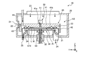
次に、処理ユニット16の概要について、図2および図3を参照しながら説明する。図2は、実施形態に係る処理ユニット16の構成を示す上面図であり、図3は、図2におけるA−A線断面図である。なお、理解の容易のため、図3ではウェハWが搬入された状態を示すとともに、リードスクリュー54の図示を省略している。
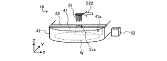
つづいて、図4A〜図4Dを参照しながら、実施形態に係る液処理の詳細について説明する。図4A〜図4Dは、実施形態に係る液処理の一工程を示す模式図(1)〜(4)である。
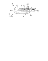
つづいて、図6〜図9Cを参照しながら、実施形態にかかる処理ユニット16の各種変形例について説明する。図6は、実施形態の変形例1に係る処理ユニット16の構成を示す上面図である。
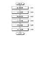
つづいて、図10および図11を参照しながら、実施形態に係る液処理の詳細について説明する。図10は、実施形態に係る液処理全体の処理手順を示すフローチャートである。
L 処理液
1 基板処理システム
16 処理ユニット(基板処理装置の一例)
17 基板搬送装置
20 筐体
21 搬入出口
30 基板処理部
31 基板保持部
32 支柱部
33 液受けカップ
34 回収カップ
40 隔壁部
41 天板部
41a 貫通孔
41b 凸部
42 側壁部
43 隙間埋め部
44 ガス供給部
45 流入抑制部
50 液供給部
51 処理液ノズル
53 アーム
55 スキャン天板
A1 第1空間
A2 第2空間
Claims (12)
- 基板を保持する基板保持部と、
前記基板保持部に保持された前記基板に向かい合って設けられ、少なくとも前記基板の中心に対向する位置に貫通孔が形成される天板部と、
前記基板保持部と前記天板部との間の空間に雰囲気を調整する雰囲気調整ガスを供給するガス供給部と、
前記基板を処理する処理液を前記基板に吐出する処理液ノズルと、
前記処理液ノズルを保持し、前記処理液ノズルから前記貫通孔を介して前記処理液を吐出する処理位置と前記基板より外方の待機位置との間で移動させるアームと、
を備える基板処理装置。 - 前記天板部は、前記基板と前記天板部との間の空間に前記貫通孔を経由して前記雰囲気調整ガスとは異なるガスが流入することを抑制する流入抑制部を有する請求項1に記載の基板処理装置。
- 前記貫通孔は、スリット状である請求項1または2に記載の基板処理装置。
- スリット状の前記貫通孔を覆うように配置され、前記処理液ノズルと同期して前記基板上でスキャンされるスキャン天板をさらに備える請求項3に記載の基板処理装置。
- 前記基板保持部が複数並んで設けられ、
前記天板部は、複数の前記基板保持部を覆うように配置され、複数の前記基板保持部上で回動可能である請求項1〜4のいずれか一つに記載の基板処理装置。 - 前記天板部は、前記基板に向かって突出する凸部を有し、
前記凸部の外径は、前記基板の外径より大きい請求項1〜5のいずれか一つに記載の基板処理装置。 - 前記基板保持部の外縁部を取り囲むように配置され、液処理された前記処理液を受ける液受けカップをさらに備え、
前記液受けカップの内径は、前記凸部の外径より大きい請求項6に記載の基板処理装置。 - 基板を保持する基板保持部と前記基板保持部と向かい合って設けられる天板部との間の空間に雰囲気を調整する雰囲気調整ガスを供給する工程と、
前記基板保持部で前記基板を保持する工程と、
前記天板部に形成された貫通孔を用いて前記基板に処理液を供給して液処理する工程と、
を含む基板処理方法。 - 前記処理液を吐出する処理液ノズルを前記貫通孔に挿通する工程をさらに含む請求項8に記載の基板処理方法。
- 前記基板保持部に保持された前記基板に前記天板部を近接させる工程をさらに含む請求項8または9に記載の基板処理方法。
- 前記液処理する工程は、前記天板部と前記基板との間を前記処理液で満たす請求項8〜10のいずれか一つに記載の基板処理方法。
- 請求項8〜11のいずれか一つに記載の基板処理方法をコンピュータに実行させる、プログラムを記憶した記憶媒体。
Priority Applications (5)
| Application Number | Priority Date | Filing Date | Title |
|---|---|---|---|
| JP2018093939A JP7090468B2 (ja) | 2018-05-15 | 2018-05-15 | 基板処理装置および基板処理方法 |
| TW108115494A TWI791109B (zh) | 2018-05-15 | 2019-05-06 | 基板處理裝置及基板處理方法 |
| US16/407,245 US10892176B2 (en) | 2018-05-15 | 2019-05-09 | Substrate processing apparatus having top plate with through hole and substrate processing method |
| KR1020190054155A KR102679000B1 (ko) | 2018-05-15 | 2019-05-09 | 기판 처리 장치 및 기판 처리 방법 |
| CN201910392650.8A CN110491799B (zh) | 2018-05-15 | 2019-05-13 | 基片处理装置和基片处理方法 |
Applications Claiming Priority (1)
| Application Number | Priority Date | Filing Date | Title |
|---|---|---|---|
| JP2018093939A JP7090468B2 (ja) | 2018-05-15 | 2018-05-15 | 基板処理装置および基板処理方法 |
Publications (2)
| Publication Number | Publication Date |
|---|---|
| JP2019201075A true JP2019201075A (ja) | 2019-11-21 |
| JP7090468B2 JP7090468B2 (ja) | 2022-06-24 |
Family
ID=68532491
Family Applications (1)
| Application Number | Title | Priority Date | Filing Date |
|---|---|---|---|
| JP2018093939A Active JP7090468B2 (ja) | 2018-05-15 | 2018-05-15 | 基板処理装置および基板処理方法 |
Country Status (5)
| Country | Link |
|---|---|
| US (1) | US10892176B2 (ja) |
| JP (1) | JP7090468B2 (ja) |
| KR (1) | KR102679000B1 (ja) |
| CN (1) | CN110491799B (ja) |
| TW (1) | TWI791109B (ja) |
Cited By (1)
| Publication number | Priority date | Publication date | Assignee | Title |
|---|---|---|---|---|
| US11373883B2 (en) * | 2018-06-29 | 2022-06-28 | Tokyo Electron Limited | Substrate processing apparatus, substrate processing system and substrate processing method |
Families Citing this family (1)
| Publication number | Priority date | Publication date | Assignee | Title |
|---|---|---|---|---|
| KR102766167B1 (ko) * | 2022-02-01 | 2025-02-10 | 시바우라 메카트로닉스 가부시끼가이샤 | 기판 처리 장치 및 기판 처리 방법 |
Citations (8)
| Publication number | Priority date | Publication date | Assignee | Title |
|---|---|---|---|---|
| JP2000012458A (ja) * | 1998-06-11 | 2000-01-14 | Samsung Electron Co Ltd | ノズル及びスピンチャックを備える半導体素子製造装置 |
| JP2001176765A (ja) * | 1999-12-20 | 2001-06-29 | Tokyo Electron Ltd | 膜形成装置 |
| JP2002368066A (ja) * | 2001-06-06 | 2002-12-20 | Tokyo Electron Ltd | 処理装置 |
| JP2008047629A (ja) * | 2006-08-11 | 2008-02-28 | Dainippon Screen Mfg Co Ltd | 基板処理装置および基板処理方法 |
| JP2012204451A (ja) * | 2011-03-24 | 2012-10-22 | Dainippon Screen Mfg Co Ltd | 基板処理装置 |
| JP2013030613A (ja) * | 2011-07-28 | 2013-02-07 | Dainippon Screen Mfg Co Ltd | 基板処理装置および基板処理方法 |
| JP2015162557A (ja) * | 2014-02-27 | 2015-09-07 | 株式会社Screenホールディングス | 基板処理装置および基板処理方法 |
| US20150343484A1 (en) * | 2014-05-28 | 2015-12-03 | Spintrac Systems, Inc. | Removable spin chamber with vacuum attachment |
Family Cites Families (24)
| Publication number | Priority date | Publication date | Assignee | Title |
|---|---|---|---|---|
| US6676757B2 (en) * | 1999-12-17 | 2004-01-13 | Tokyo Electron Limited | Coating film forming apparatus and coating unit |
| JP2001319845A (ja) | 2000-05-02 | 2001-11-16 | Tokyo Electron Ltd | 塗布現像処理システム |
| US6811613B2 (en) * | 2001-11-26 | 2004-11-02 | Tokyo Electron Limited | Coating film forming apparatus |
| JP4565433B2 (ja) * | 2001-11-27 | 2010-10-20 | 東京エレクトロン株式会社 | 液処理装置および液処理方法 |
| JP2004006672A (ja) * | 2002-04-19 | 2004-01-08 | Dainippon Screen Mfg Co Ltd | 基板処理方法および基板処理装置 |
| JP4112923B2 (ja) * | 2002-07-22 | 2008-07-02 | 芝浦メカトロニクス株式会社 | 基板の処理装置及び処理方法 |
| JP3824567B2 (ja) * | 2002-09-30 | 2006-09-20 | 株式会社荏原製作所 | 基板処理装置 |
| JP4865208B2 (ja) * | 2004-11-12 | 2012-02-01 | シャープ株式会社 | 大気圧プラズマ処理装置 |
| US7914626B2 (en) * | 2005-11-24 | 2011-03-29 | Tokyo Electron Limited | Liquid processing method and liquid processing apparatus |
| JP2007157898A (ja) * | 2005-12-02 | 2007-06-21 | Tokyo Electron Ltd | 基板洗浄方法、基板洗浄装置、制御プログラム、およびコンピュータ読取可能な記憶媒体 |
| JP4760516B2 (ja) * | 2005-12-15 | 2011-08-31 | 東京エレクトロン株式会社 | 塗布装置及び塗布方法 |
| JP4762098B2 (ja) * | 2006-09-28 | 2011-08-31 | 大日本スクリーン製造株式会社 | 基板処理装置および基板処理方法 |
| JP5067432B2 (ja) * | 2010-02-15 | 2012-11-07 | 東京エレクトロン株式会社 | 塗布、現像装置、現像方法及び記憶媒体 |
| JP5789546B2 (ja) * | 2011-04-26 | 2015-10-07 | 東京エレクトロン株式会社 | 塗布処理装置、塗布現像処理システム、並びに塗布処理方法及びその塗布処理方法を実行させるためのプログラムを記録した記録媒体 |
| JP2013062361A (ja) * | 2011-09-13 | 2013-04-04 | Tokyo Electron Ltd | 熱処理装置、温度制御システム、熱処理方法、温度制御方法及びその熱処理方法又はその温度制御方法を実行させるためのプログラムを記録した記録媒体 |
| JP5829092B2 (ja) * | 2011-10-13 | 2015-12-09 | 東京エレクトロン株式会社 | 液処理装置および液処理方法 |
| JP5666414B2 (ja) * | 2011-10-27 | 2015-02-12 | 東京エレクトロン株式会社 | 液処理装置、液処理方法および記憶媒体 |
| US8703403B2 (en) * | 2011-12-22 | 2014-04-22 | Taiwan Semiconductor Manufacturing Company, Ltd. | Method and apparatus for drying a wafer |
| JP6090837B2 (ja) * | 2012-06-13 | 2017-03-08 | 株式会社Screenホールディングス | 基板処理装置および基板処理方法 |
| KR101512560B1 (ko) * | 2012-08-31 | 2015-04-15 | 가부시키가이샤 스크린 홀딩스 | 기판처리장치 |
| JP2014204018A (ja) * | 2013-04-08 | 2014-10-27 | シンフォニアテクノロジー株式会社 | 被処理体の冷却ユニット |
| JP6032189B2 (ja) * | 2013-12-03 | 2016-11-24 | 東京エレクトロン株式会社 | 塗布膜形成装置、塗布膜形成方法、記憶媒体 |
| EP3112018A1 (en) * | 2015-07-02 | 2017-01-04 | Centrillion Technology Holdings Corporation | Systems and methods to dispense and mix reagents |
| JP6670674B2 (ja) * | 2016-05-18 | 2020-03-25 | 株式会社Screenホールディングス | 基板処理装置および基板処理方法 |
-
2018
- 2018-05-15 JP JP2018093939A patent/JP7090468B2/ja active Active
-
2019
- 2019-05-06 TW TW108115494A patent/TWI791109B/zh active
- 2019-05-09 KR KR1020190054155A patent/KR102679000B1/ko active Active
- 2019-05-09 US US16/407,245 patent/US10892176B2/en active Active
- 2019-05-13 CN CN201910392650.8A patent/CN110491799B/zh active Active
Patent Citations (8)
| Publication number | Priority date | Publication date | Assignee | Title |
|---|---|---|---|---|
| JP2000012458A (ja) * | 1998-06-11 | 2000-01-14 | Samsung Electron Co Ltd | ノズル及びスピンチャックを備える半導体素子製造装置 |
| JP2001176765A (ja) * | 1999-12-20 | 2001-06-29 | Tokyo Electron Ltd | 膜形成装置 |
| JP2002368066A (ja) * | 2001-06-06 | 2002-12-20 | Tokyo Electron Ltd | 処理装置 |
| JP2008047629A (ja) * | 2006-08-11 | 2008-02-28 | Dainippon Screen Mfg Co Ltd | 基板処理装置および基板処理方法 |
| JP2012204451A (ja) * | 2011-03-24 | 2012-10-22 | Dainippon Screen Mfg Co Ltd | 基板処理装置 |
| JP2013030613A (ja) * | 2011-07-28 | 2013-02-07 | Dainippon Screen Mfg Co Ltd | 基板処理装置および基板処理方法 |
| JP2015162557A (ja) * | 2014-02-27 | 2015-09-07 | 株式会社Screenホールディングス | 基板処理装置および基板処理方法 |
| US20150343484A1 (en) * | 2014-05-28 | 2015-12-03 | Spintrac Systems, Inc. | Removable spin chamber with vacuum attachment |
Cited By (1)
| Publication number | Priority date | Publication date | Assignee | Title |
|---|---|---|---|---|
| US11373883B2 (en) * | 2018-06-29 | 2022-06-28 | Tokyo Electron Limited | Substrate processing apparatus, substrate processing system and substrate processing method |
Also Published As
| Publication number | Publication date |
|---|---|
| CN110491799B (zh) | 2024-04-02 |
| CN110491799A (zh) | 2019-11-22 |
| KR20190130963A (ko) | 2019-11-25 |
| TW201947689A (zh) | 2019-12-16 |
| TWI791109B (zh) | 2023-02-01 |
| JP7090468B2 (ja) | 2022-06-24 |
| KR102679000B1 (ko) | 2024-06-26 |
| US20190355593A1 (en) | 2019-11-21 |
| US10892176B2 (en) | 2021-01-12 |
Similar Documents
| Publication | Publication Date | Title |
|---|---|---|
| US9305767B2 (en) | Liquid processing apparatus, liquid processing method and storage medium | |
| US20200168482A1 (en) | Substrate processing apparatus and substrate processing method | |
| JP7337175B2 (ja) | 基板処理装置および基板処理方法 | |
| KR102294642B1 (ko) | 액 처리 장치 | |
| US20230352328A1 (en) | Substrate processing method and substrate processing apparatus | |
| JP2019201075A (ja) | 基板処理装置および基板処理方法 | |
| JP7213624B2 (ja) | 基板処理装置、基板処理システムおよび基板処理方法 | |
| US11373883B2 (en) | Substrate processing apparatus, substrate processing system and substrate processing method | |
| JP5726637B2 (ja) | 液処理装置、液処理方法 | |
| JP4688533B2 (ja) | 基板処理装置 | |
| JP5726636B2 (ja) | 液処理装置、液処理方法 | |
| JPWO2019012978A1 (ja) | 基板搬送装置および基板搬送方法 | |
| JP2025081012A (ja) | 基板処理方法および基板処理装置 | |
| CN119852204A (zh) | 制造方法、基板加工方法和基板加工装置 |
Legal Events
| Date | Code | Title | Description |
|---|---|---|---|
| A621 | Written request for application examination |
Free format text: JAPANESE INTERMEDIATE CODE: A621 Effective date: 20210312 |
|
| A977 | Report on retrieval |
Free format text: JAPANESE INTERMEDIATE CODE: A971007 Effective date: 20220113 |
|
| A131 | Notification of reasons for refusal |
Free format text: JAPANESE INTERMEDIATE CODE: A131 Effective date: 20220118 |
|
| A521 | Request for written amendment filed |
Free format text: JAPANESE INTERMEDIATE CODE: A523 Effective date: 20220225 |
|
| TRDD | Decision of grant or rejection written | ||
| A01 | Written decision to grant a patent or to grant a registration (utility model) |
Free format text: JAPANESE INTERMEDIATE CODE: A01 Effective date: 20220517 |
|
| A61 | First payment of annual fees (during grant procedure) |
Free format text: JAPANESE INTERMEDIATE CODE: A61 Effective date: 20220614 |
|
| R150 | Certificate of patent or registration of utility model |
Ref document number: 7090468 Country of ref document: JP Free format text: JAPANESE INTERMEDIATE CODE: R150 |
|
| R250 | Receipt of annual fees |
Free format text: JAPANESE INTERMEDIATE CODE: R250 |