JP2019201077A - 半導体装置 - Google Patents
半導体装置 Download PDFInfo
- Publication number
- JP2019201077A JP2019201077A JP2018093960A JP2018093960A JP2019201077A JP 2019201077 A JP2019201077 A JP 2019201077A JP 2018093960 A JP2018093960 A JP 2018093960A JP 2018093960 A JP2018093960 A JP 2018093960A JP 2019201077 A JP2019201077 A JP 2019201077A
- Authority
- JP
- Japan
- Prior art keywords
- signal
- semiconductor element
- signal terminal
- electrodes
- terminal
- Prior art date
- Legal status (The legal status is an assumption and is not a legal conclusion. Google has not performed a legal analysis and makes no representation as to the accuracy of the status listed.)
- Granted
Links
Images




Classifications
-
- H—ELECTRICITY
- H10—SEMICONDUCTOR DEVICES; ELECTRIC SOLID-STATE DEVICES NOT OTHERWISE PROVIDED FOR
- H10W—GENERIC PACKAGES, INTERCONNECTIONS, CONNECTORS OR OTHER CONSTRUCTIONAL DETAILS OF DEVICES COVERED BY CLASS H10
- H10W90/00—Package configurations
- H10W90/701—Package configurations characterised by the relative positions of pads or connectors relative to package parts
-
- H—ELECTRICITY
- H10—SEMICONDUCTOR DEVICES; ELECTRIC SOLID-STATE DEVICES NOT OTHERWISE PROVIDED FOR
- H10W—GENERIC PACKAGES, INTERCONNECTIONS, CONNECTORS OR OTHER CONSTRUCTIONAL DETAILS OF DEVICES COVERED BY CLASS H10
- H10W40/00—Arrangements for thermal protection or thermal control
- H10W40/70—Fillings or auxiliary members in containers or in encapsulations for thermal protection or control
- H10W40/77—Auxiliary members characterised by their shape
- H10W40/778—Auxiliary members characterised by their shape in encapsulations
-
- H—ELECTRICITY
- H10—SEMICONDUCTOR DEVICES; ELECTRIC SOLID-STATE DEVICES NOT OTHERWISE PROVIDED FOR
- H10W—GENERIC PACKAGES, INTERCONNECTIONS, CONNECTORS OR OTHER CONSTRUCTIONAL DETAILS OF DEVICES COVERED BY CLASS H10
- H10W70/00—Package substrates; Interposers; Redistribution layers [RDL]
- H10W70/40—Leadframes
-
- H—ELECTRICITY
- H10—SEMICONDUCTOR DEVICES; ELECTRIC SOLID-STATE DEVICES NOT OTHERWISE PROVIDED FOR
- H10W—GENERIC PACKAGES, INTERCONNECTIONS, CONNECTORS OR OTHER CONSTRUCTIONAL DETAILS OF DEVICES COVERED BY CLASS H10
- H10W70/00—Package substrates; Interposers; Redistribution layers [RDL]
- H10W70/40—Leadframes
- H10W70/421—Shapes or dispositions
- H10W70/442—Shapes or dispositions of multiple leadframes in a single chip
-
- H—ELECTRICITY
- H10—SEMICONDUCTOR DEVICES; ELECTRIC SOLID-STATE DEVICES NOT OTHERWISE PROVIDED FOR
- H10W—GENERIC PACKAGES, INTERCONNECTIONS, CONNECTORS OR OTHER CONSTRUCTIONAL DETAILS OF DEVICES COVERED BY CLASS H10
- H10W70/00—Package substrates; Interposers; Redistribution layers [RDL]
- H10W70/40—Leadframes
- H10W70/464—Additional interconnections in combination with leadframes
- H10W70/468—Circuit boards
-
- H—ELECTRICITY
- H10—SEMICONDUCTOR DEVICES; ELECTRIC SOLID-STATE DEVICES NOT OTHERWISE PROVIDED FOR
- H10W—GENERIC PACKAGES, INTERCONNECTIONS, CONNECTORS OR OTHER CONSTRUCTIONAL DETAILS OF DEVICES COVERED BY CLASS H10
- H10W70/00—Package substrates; Interposers; Redistribution layers [RDL]
- H10W70/40—Leadframes
- H10W70/481—Leadframes for devices being provided for in groups H10D8/00 - H10D48/00
-
- H—ELECTRICITY
- H10—SEMICONDUCTOR DEVICES; ELECTRIC SOLID-STATE DEVICES NOT OTHERWISE PROVIDED FOR
- H10W—GENERIC PACKAGES, INTERCONNECTIONS, CONNECTORS OR OTHER CONSTRUCTIONAL DETAILS OF DEVICES COVERED BY CLASS H10
- H10W72/00—Interconnections or connectors in packages
- H10W72/50—Bond wires
-
- H—ELECTRICITY
- H10—SEMICONDUCTOR DEVICES; ELECTRIC SOLID-STATE DEVICES NOT OTHERWISE PROVIDED FOR
- H10W—GENERIC PACKAGES, INTERCONNECTIONS, CONNECTORS OR OTHER CONSTRUCTIONAL DETAILS OF DEVICES COVERED BY CLASS H10
- H10W72/00—Interconnections or connectors in packages
- H10W72/60—Strap connectors, e.g. thick copper clips for grounding of power devices
-
- H—ELECTRICITY
- H10—SEMICONDUCTOR DEVICES; ELECTRIC SOLID-STATE DEVICES NOT OTHERWISE PROVIDED FOR
- H10W—GENERIC PACKAGES, INTERCONNECTIONS, CONNECTORS OR OTHER CONSTRUCTIONAL DETAILS OF DEVICES COVERED BY CLASS H10
- H10W74/00—Encapsulations, e.g. protective coatings
- H10W74/10—Encapsulations, e.g. protective coatings characterised by their shape or disposition
- H10W74/111—Encapsulations, e.g. protective coatings characterised by their shape or disposition the semiconductor body being completely enclosed
- H10W74/114—Encapsulations, e.g. protective coatings characterised by their shape or disposition the semiconductor body being completely enclosed by a substrate and the encapsulations
-
- H—ELECTRICITY
- H10—SEMICONDUCTOR DEVICES; ELECTRIC SOLID-STATE DEVICES NOT OTHERWISE PROVIDED FOR
- H10W—GENERIC PACKAGES, INTERCONNECTIONS, CONNECTORS OR OTHER CONSTRUCTIONAL DETAILS OF DEVICES COVERED BY CLASS H10
- H10W90/00—Package configurations
-
- H—ELECTRICITY
- H10—SEMICONDUCTOR DEVICES; ELECTRIC SOLID-STATE DEVICES NOT OTHERWISE PROVIDED FOR
- H10W—GENERIC PACKAGES, INTERCONNECTIONS, CONNECTORS OR OTHER CONSTRUCTIONAL DETAILS OF DEVICES COVERED BY CLASS H10
- H10W90/00—Package configurations
- H10W90/811—Multiple chips on leadframes
-
- H—ELECTRICITY
- H10—SEMICONDUCTOR DEVICES; ELECTRIC SOLID-STATE DEVICES NOT OTHERWISE PROVIDED FOR
- H10W—GENERIC PACKAGES, INTERCONNECTIONS, CONNECTORS OR OTHER CONSTRUCTIONAL DETAILS OF DEVICES COVERED BY CLASS H10
- H10W40/00—Arrangements for thermal protection or thermal control
- H10W40/20—Arrangements for cooling
- H10W40/25—Arrangements for cooling characterised by their materials
- H10W40/255—Arrangements for cooling characterised by their materials having a laminate or multilayered structure, e.g. direct bond copper [DBC] ceramic substrates
-
- H—ELECTRICITY
- H10—SEMICONDUCTOR DEVICES; ELECTRIC SOLID-STATE DEVICES NOT OTHERWISE PROVIDED FOR
- H10W—GENERIC PACKAGES, INTERCONNECTIONS, CONNECTORS OR OTHER CONSTRUCTIONAL DETAILS OF DEVICES COVERED BY CLASS H10
- H10W72/00—Interconnections or connectors in packages
- H10W72/071—Connecting or disconnecting
- H10W72/073—Connecting or disconnecting of die-attach connectors
- H10W72/07331—Connecting techniques
- H10W72/07336—Soldering or alloying
-
- H—ELECTRICITY
- H10—SEMICONDUCTOR DEVICES; ELECTRIC SOLID-STATE DEVICES NOT OTHERWISE PROVIDED FOR
- H10W—GENERIC PACKAGES, INTERCONNECTIONS, CONNECTORS OR OTHER CONSTRUCTIONAL DETAILS OF DEVICES COVERED BY CLASS H10
- H10W72/00—Interconnections or connectors in packages
- H10W72/071—Connecting or disconnecting
- H10W72/073—Connecting or disconnecting of die-attach connectors
- H10W72/07351—Connecting or disconnecting of die-attach connectors characterised by changes in properties of the die-attach connectors during connecting
- H10W72/07354—Connecting or disconnecting of die-attach connectors characterised by changes in properties of the die-attach connectors during connecting changes in dispositions
-
- H—ELECTRICITY
- H10—SEMICONDUCTOR DEVICES; ELECTRIC SOLID-STATE DEVICES NOT OTHERWISE PROVIDED FOR
- H10W—GENERIC PACKAGES, INTERCONNECTIONS, CONNECTORS OR OTHER CONSTRUCTIONAL DETAILS OF DEVICES COVERED BY CLASS H10
- H10W72/00—Interconnections or connectors in packages
- H10W72/30—Die-attach connectors
- H10W72/341—Dispositions of die-attach connectors, e.g. layouts
- H10W72/347—Dispositions of multiple die-attach connectors
-
- H—ELECTRICITY
- H10—SEMICONDUCTOR DEVICES; ELECTRIC SOLID-STATE DEVICES NOT OTHERWISE PROVIDED FOR
- H10W—GENERIC PACKAGES, INTERCONNECTIONS, CONNECTORS OR OTHER CONSTRUCTIONAL DETAILS OF DEVICES COVERED BY CLASS H10
- H10W72/00—Interconnections or connectors in packages
- H10W72/30—Die-attach connectors
- H10W72/351—Materials of die-attach connectors
- H10W72/352—Materials of die-attach connectors comprising metals or metalloids, e.g. solders
-
- H—ELECTRICITY
- H10—SEMICONDUCTOR DEVICES; ELECTRIC SOLID-STATE DEVICES NOT OTHERWISE PROVIDED FOR
- H10W—GENERIC PACKAGES, INTERCONNECTIONS, CONNECTORS OR OTHER CONSTRUCTIONAL DETAILS OF DEVICES COVERED BY CLASS H10
- H10W72/00—Interconnections or connectors in packages
- H10W72/30—Die-attach connectors
- H10W72/381—Auxiliary members
-
- H—ELECTRICITY
- H10—SEMICONDUCTOR DEVICES; ELECTRIC SOLID-STATE DEVICES NOT OTHERWISE PROVIDED FOR
- H10W—GENERIC PACKAGES, INTERCONNECTIONS, CONNECTORS OR OTHER CONSTRUCTIONAL DETAILS OF DEVICES COVERED BY CLASS H10
- H10W72/00—Interconnections or connectors in packages
- H10W72/50—Bond wires
- H10W72/541—Dispositions of bond wires
- H10W72/5449—Dispositions of bond wires not being orthogonal to a side surface of the chip, e.g. fan-out arrangements
-
- H—ELECTRICITY
- H10—SEMICONDUCTOR DEVICES; ELECTRIC SOLID-STATE DEVICES NOT OTHERWISE PROVIDED FOR
- H10W—GENERIC PACKAGES, INTERCONNECTIONS, CONNECTORS OR OTHER CONSTRUCTIONAL DETAILS OF DEVICES COVERED BY CLASS H10
- H10W72/00—Interconnections or connectors in packages
- H10W72/851—Dispositions of multiple connectors or interconnections
- H10W72/853—On the same surface
- H10W72/871—Bond wires and strap connectors
-
- H—ELECTRICITY
- H10—SEMICONDUCTOR DEVICES; ELECTRIC SOLID-STATE DEVICES NOT OTHERWISE PROVIDED FOR
- H10W—GENERIC PACKAGES, INTERCONNECTIONS, CONNECTORS OR OTHER CONSTRUCTIONAL DETAILS OF DEVICES COVERED BY CLASS H10
- H10W72/00—Interconnections or connectors in packages
- H10W72/851—Dispositions of multiple connectors or interconnections
- H10W72/874—On different surfaces
- H10W72/884—Die-attach connectors and bond wires
-
- H—ELECTRICITY
- H10—SEMICONDUCTOR DEVICES; ELECTRIC SOLID-STATE DEVICES NOT OTHERWISE PROVIDED FOR
- H10W—GENERIC PACKAGES, INTERCONNECTIONS, CONNECTORS OR OTHER CONSTRUCTIONAL DETAILS OF DEVICES COVERED BY CLASS H10
- H10W72/00—Interconnections or connectors in packages
- H10W72/90—Bond pads, in general
- H10W72/921—Structures or relative sizes of bond pads
- H10W72/926—Multiple bond pads having different sizes
-
- H—ELECTRICITY
- H10—SEMICONDUCTOR DEVICES; ELECTRIC SOLID-STATE DEVICES NOT OTHERWISE PROVIDED FOR
- H10W—GENERIC PACKAGES, INTERCONNECTIONS, CONNECTORS OR OTHER CONSTRUCTIONAL DETAILS OF DEVICES COVERED BY CLASS H10
- H10W72/00—Interconnections or connectors in packages
- H10W72/90—Bond pads, in general
- H10W72/931—Shapes of bond pads
- H10W72/932—Plan-view shape, i.e. in top view
-
- H—ELECTRICITY
- H10—SEMICONDUCTOR DEVICES; ELECTRIC SOLID-STATE DEVICES NOT OTHERWISE PROVIDED FOR
- H10W—GENERIC PACKAGES, INTERCONNECTIONS, CONNECTORS OR OTHER CONSTRUCTIONAL DETAILS OF DEVICES COVERED BY CLASS H10
- H10W72/00—Interconnections or connectors in packages
- H10W72/90—Bond pads, in general
- H10W72/941—Dispositions of bond pads
- H10W72/944—Dispositions of multiple bond pads
-
- H—ELECTRICITY
- H10—SEMICONDUCTOR DEVICES; ELECTRIC SOLID-STATE DEVICES NOT OTHERWISE PROVIDED FOR
- H10W—GENERIC PACKAGES, INTERCONNECTIONS, CONNECTORS OR OTHER CONSTRUCTIONAL DETAILS OF DEVICES COVERED BY CLASS H10
- H10W74/00—Encapsulations, e.g. protective coatings
-
- H—ELECTRICITY
- H10—SEMICONDUCTOR DEVICES; ELECTRIC SOLID-STATE DEVICES NOT OTHERWISE PROVIDED FOR
- H10W—GENERIC PACKAGES, INTERCONNECTIONS, CONNECTORS OR OTHER CONSTRUCTIONAL DETAILS OF DEVICES COVERED BY CLASS H10
- H10W74/00—Encapsulations, e.g. protective coatings
- H10W74/10—Encapsulations, e.g. protective coatings characterised by their shape or disposition
- H10W74/111—Encapsulations, e.g. protective coatings characterised by their shape or disposition the semiconductor body being completely enclosed
-
- H—ELECTRICITY
- H10—SEMICONDUCTOR DEVICES; ELECTRIC SOLID-STATE DEVICES NOT OTHERWISE PROVIDED FOR
- H10W—GENERIC PACKAGES, INTERCONNECTIONS, CONNECTORS OR OTHER CONSTRUCTIONAL DETAILS OF DEVICES COVERED BY CLASS H10
- H10W76/00—Containers; Fillings or auxiliary members therefor; Seals
- H10W76/10—Containers or parts thereof
- H10W76/12—Containers or parts thereof characterised by their shape
- H10W76/13—Containers comprising a conductive base serving as an interconnection
- H10W76/138—Containers comprising a conductive base serving as an interconnection having another interconnection being formed by a cover plate parallel to the conductive base, e.g. sandwich type
-
- H—ELECTRICITY
- H10—SEMICONDUCTOR DEVICES; ELECTRIC SOLID-STATE DEVICES NOT OTHERWISE PROVIDED FOR
- H10W—GENERIC PACKAGES, INTERCONNECTIONS, CONNECTORS OR OTHER CONSTRUCTIONAL DETAILS OF DEVICES COVERED BY CLASS H10
- H10W90/00—Package configurations
- H10W90/701—Package configurations characterised by the relative positions of pads or connectors relative to package parts
- H10W90/731—Package configurations characterised by the relative positions of pads or connectors relative to package parts of die-attach connectors
- H10W90/736—Package configurations characterised by the relative positions of pads or connectors relative to package parts of die-attach connectors between a chip and a stacked lead frame, conducting package substrate or heat sink
-
- H—ELECTRICITY
- H10—SEMICONDUCTOR DEVICES; ELECTRIC SOLID-STATE DEVICES NOT OTHERWISE PROVIDED FOR
- H10W—GENERIC PACKAGES, INTERCONNECTIONS, CONNECTORS OR OTHER CONSTRUCTIONAL DETAILS OF DEVICES COVERED BY CLASS H10
- H10W90/00—Package configurations
- H10W90/701—Package configurations characterised by the relative positions of pads or connectors relative to package parts
- H10W90/751—Package configurations characterised by the relative positions of pads or connectors relative to package parts of bond wires
- H10W90/756—Package configurations characterised by the relative positions of pads or connectors relative to package parts of bond wires between a chip and a stacked lead frame, conducting package substrate or heat sink
-
- H—ELECTRICITY
- H10—SEMICONDUCTOR DEVICES; ELECTRIC SOLID-STATE DEVICES NOT OTHERWISE PROVIDED FOR
- H10W—GENERIC PACKAGES, INTERCONNECTIONS, CONNECTORS OR OTHER CONSTRUCTIONAL DETAILS OF DEVICES COVERED BY CLASS H10
- H10W90/00—Package configurations
- H10W90/701—Package configurations characterised by the relative positions of pads or connectors relative to package parts
- H10W90/761—Package configurations characterised by the relative positions of pads or connectors relative to package parts of strap connectors
- H10W90/763—Package configurations characterised by the relative positions of pads or connectors relative to package parts of strap connectors between laterally-adjacent chips
Landscapes
- Inverter Devices (AREA)
- Engineering & Computer Science (AREA)
- Microelectronics & Electronic Packaging (AREA)
- Power Conversion In General (AREA)
- Semiconductor Integrated Circuits (AREA)
Abstract
Description
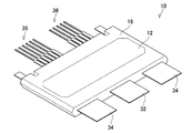
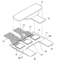
12:第1導体板
14:第2導体板
16:封止体
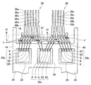
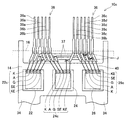
22、24、26:半導体素子
22a、24a、26a:上面電極
22b、24b、24c:下面電極
22c、24c、26c:信号電極
28:温度センサ
30:電流センサ
32:第1電力端子
34:第2電力端子
36:信号端子
36a:第1信号端子
36b:第2信号端子
36c:第3信号端子
36d:共通信号端子
37:側方延伸部
38:支持部
40:ボンディングワイヤ
K:第2温度信号電極
A:第1温度信号電極
G:ゲート信号電極
SE:電流信号電極
KE:基準電圧信号電極
Claims (10)
- 複数の信号電極を有する第1半導体素子と、
複数の信号電極を有する第2半導体素子と、
前記第1半導体素子及び前記第2半導体素子を封止する封止体と、
前記封止体から突出する複数の信号端子と、を備え、
前記複数の信号端子には、第1信号端子と、第2信号端子と、共通信号端子が含まれており、
前記第1信号端子は、前記封止体の内部において、前記第1半導体素子の前記複数の信号電極の一つに接続されており、
前記第2信号端子は、前記封止体の内部において、前記第2半導体素子の前記複数の信号電極の一つに接続されており、
前記共通信号端子は、前記封止体の内部において、前記第1半導体素子の前記複数の信号電極の他の一つと、前記第2半導体素子の前記複数の信号電極の他の一つとの両者に接続されている、
半導体装置。 - 前記共通信号端子は、前記複数の信号端子の配列方向に沿って延びる側方延伸部を、前記封止体の内部に有する、請求項1に記載の半導体装置。
- 前記側方延伸部は、前記共通信号端子に隣接する他の前記信号端子の反対側まで延びる、請求項2に記載の半導体装置。
- 前記側方延伸部は、前記共通信号端子に隣接する他の前記信号端子と立体交差する、請求項3に記載の半導体装置。
- 前記側方延伸部は、前記共通信号端子に隣接する他の前記信号端子と、当該他の信号端子が接続された前記第1半導体素子又は前記第2半導体素子との間に位置する、請求項3に記載の半導体装置。
- 前記封止体の内部において前記側方延伸部に接続された支持部をさらに有し、
前記支持部は、前記第1信号端子と前記第2信号端子の間において、前記封止体から突出している、請求項2から5のいずれか一項に記載の半導体装置。 - 前記封止体によって封止されているとともに、複数の信号電極を有する第3半導体素子をさらに備え、
前記共通信号端子は、前記封止体の内部において、前記第3半導体素子の前記複数の信号電極の一つにさらに接続されている、請求項1から6のいずれか一項に記載の半導体装置。 - 前記第1半導体素子と前記第2半導体素子とのそれぞれは、温度検出部を有し、
前記第1半導体素子の前記複数の信号電極と、前記第2半導体素子の前記複数の信号電極とのそれぞれは、前記温度検出部の一端に接続された第1温度信号電極と、前記温度検出部の他端に接続された第2温度信号電極とを有し、
前記第1信号端子は、前記第1半導体素子の前記第1温度信号電極に接続されており、
前記第2信号端子は、前記第2半導体素子の前記第1温度信号電極に接続されており、
前記共通信号端子は、前記第1半導体素子の前記第2温度信号電極と、前記第2半導体素子の前記第2温度信号電極との両者に接続されている、請求項1から7のいずれか一項に記載の半導体装置。 - 前記第1半導体素子と前記第2半導体素子とのそれぞれは、電流検出部を有し、
前記第1半導体素子の前記複数の信号電極と、前記第2半導体素子の前記複数の信号電極とのそれぞれは、前記電流検出部の一端に接続された電流信号電極と、前記電流信号電極が出力する信号に対する基準電圧を出力する基準電圧信号電極とを有し、
前記第1信号端子は、前記第1半導体素子の前記電流信号電極に接続されており、
前記第2信号端子は、前記第2半導体素子の前記電流信号電極に接続されており、
前記共通信号端子は、前記第1半導体素子の前記基準電圧信号電極と、前記第2半導体素子の前記基準電圧信号電極との両者に接続されている、請求項1から7のいずれか一項に記載の半導体装置。 - 前記第1半導体素子と前記第2半導体素子とのそれぞれは、ゲートを有するスイッチング素子であり、
前記第1半導体素子の前記複数の信号電極と、前記第2半導体素子の前記複数の信号電極とのそれぞれは、前記ゲートに接続されたゲート信号電極を有し、
前記共通信号端子は、前記封止体の内部において、前記第1半導体素子の前記ゲート信号電極と、前記第2半導体素子の前記ゲート信号電極とに接続されている、請求項1から7のいずれか一項に記載の半導体装置。
Priority Applications (3)
| Application Number | Priority Date | Filing Date | Title |
|---|---|---|---|
| JP2018093960A JP7070070B2 (ja) | 2018-05-15 | 2018-05-15 | 半導体装置 |
| US16/383,746 US10886207B2 (en) | 2018-05-15 | 2019-04-15 | Semiconductor device |
| CN201910392954.4A CN110491841A (zh) | 2018-05-15 | 2019-05-13 | 半导体装置 |
Applications Claiming Priority (1)
| Application Number | Priority Date | Filing Date | Title |
|---|---|---|---|
| JP2018093960A JP7070070B2 (ja) | 2018-05-15 | 2018-05-15 | 半導体装置 |
Publications (2)
| Publication Number | Publication Date |
|---|---|
| JP2019201077A true JP2019201077A (ja) | 2019-11-21 |
| JP7070070B2 JP7070070B2 (ja) | 2022-05-18 |
Family
ID=68532360
Family Applications (1)
| Application Number | Title | Priority Date | Filing Date |
|---|---|---|---|
| JP2018093960A Active JP7070070B2 (ja) | 2018-05-15 | 2018-05-15 | 半導体装置 |
Country Status (3)
| Country | Link |
|---|---|
| US (1) | US10886207B2 (ja) |
| JP (1) | JP7070070B2 (ja) |
| CN (1) | CN110491841A (ja) |
Citations (4)
| Publication number | Priority date | Publication date | Assignee | Title |
|---|---|---|---|---|
| JP2003142689A (ja) * | 2001-11-01 | 2003-05-16 | Mitsubishi Electric Corp | 半導体装置 |
| WO2014046058A1 (ja) * | 2012-09-20 | 2014-03-27 | ローム株式会社 | パワーモジュール半導体装置およびインバータ装置、およびパワーモジュール半導体装置の製造方法、および金型 |
| WO2015001648A1 (ja) * | 2013-07-04 | 2015-01-08 | 三菱電機株式会社 | 半導体装置の製造方法、半導体装置 |
| WO2017169693A1 (ja) * | 2016-04-01 | 2017-10-05 | 三菱電機株式会社 | 半導体モジュール |
Family Cites Families (8)
| Publication number | Priority date | Publication date | Assignee | Title |
|---|---|---|---|---|
| JPH05218281A (ja) * | 1992-02-07 | 1993-08-27 | Texas Instr Japan Ltd | 半導体装置 |
| JP2008270293A (ja) | 2007-04-16 | 2008-11-06 | Sumitomo Electric Ind Ltd | パワーモジュール |
| JP5402456B2 (ja) | 2009-09-18 | 2014-01-29 | 富士ゼロックス株式会社 | 発光装置、プリントヘッドおよび画像形成装置 |
| JP2011086889A (ja) * | 2009-10-19 | 2011-04-28 | Renesas Electronics Corp | 半導体装置およびその製造方法 |
| JP6156131B2 (ja) | 2013-12-24 | 2017-07-05 | トヨタ自動車株式会社 | 半導体装置 |
| ITTO20150231A1 (it) * | 2015-04-24 | 2016-10-24 | St Microelectronics Srl | Procedimento per produrre lead frame per componenti elettronici, componente e prodotto informatico corrispondenti |
| JP2017147316A (ja) | 2016-02-17 | 2017-08-24 | トヨタ自動車株式会社 | 半導体装置 |
| JP6750514B2 (ja) * | 2017-01-18 | 2020-09-02 | 株式会社デンソー | 半導体装置 |
-
2018
- 2018-05-15 JP JP2018093960A patent/JP7070070B2/ja active Active
-
2019
- 2019-04-15 US US16/383,746 patent/US10886207B2/en active Active
- 2019-05-13 CN CN201910392954.4A patent/CN110491841A/zh active Pending
Patent Citations (4)
| Publication number | Priority date | Publication date | Assignee | Title |
|---|---|---|---|---|
| JP2003142689A (ja) * | 2001-11-01 | 2003-05-16 | Mitsubishi Electric Corp | 半導体装置 |
| WO2014046058A1 (ja) * | 2012-09-20 | 2014-03-27 | ローム株式会社 | パワーモジュール半導体装置およびインバータ装置、およびパワーモジュール半導体装置の製造方法、および金型 |
| WO2015001648A1 (ja) * | 2013-07-04 | 2015-01-08 | 三菱電機株式会社 | 半導体装置の製造方法、半導体装置 |
| WO2017169693A1 (ja) * | 2016-04-01 | 2017-10-05 | 三菱電機株式会社 | 半導体モジュール |
Also Published As
| Publication number | Publication date |
|---|---|
| US20190355653A1 (en) | 2019-11-21 |
| US10886207B2 (en) | 2021-01-05 |
| JP7070070B2 (ja) | 2022-05-18 |
| CN110491841A (zh) | 2019-11-22 |
Similar Documents
| Publication | Publication Date | Title |
|---|---|---|
| US20250219025A1 (en) | Semiconductor power module | |
| JP6717270B2 (ja) | 半導体モジュール | |
| JP6338937B2 (ja) | パワーモジュールおよびその製造方法 | |
| KR102156867B1 (ko) | 반도체 장치 | |
| CN111095760B (zh) | 电力转换装置 | |
| CN104919589A (zh) | 半导体装置 | |
| US10403558B2 (en) | Power module with multi-layer substrate | |
| US10903138B2 (en) | Semiconductor device and method of manufacturing the same | |
| CN110600457B (zh) | 半导体装置 | |
| JP2019186403A (ja) | 半導体装置 | |
| US10950526B2 (en) | Semiconductor device | |
| US10964630B2 (en) | Semiconductor device having a conductor plate and semiconductor elements | |
| JP2007116172A (ja) | パワー半導体モジュール | |
| US11274972B2 (en) | Semiconductor device | |
| JP7192235B2 (ja) | 半導体装置 | |
| JP7070070B2 (ja) | 半導体装置 | |
| JP2005252305A (ja) | 電力用半導体装置 | |
| JP7139799B2 (ja) | 半導体装置 | |
| JP7159609B2 (ja) | 半導体装置 | |
| CN111952260B (zh) | 半导体装置 | |
| JP2020188167A (ja) | 半導体装置 | |
| JP2008054495A (ja) | 電流印加されたパワー回路のための低インダクタンスのパワー半導体モジュール |
Legal Events
| Date | Code | Title | Description |
|---|---|---|---|
| A711 | Notification of change in applicant |
Free format text: JAPANESE INTERMEDIATE CODE: A711 Effective date: 20200401 |
|
| A621 | Written request for application examination |
Free format text: JAPANESE INTERMEDIATE CODE: A621 Effective date: 20210218 |
|
| A977 | Report on retrieval |
Free format text: JAPANESE INTERMEDIATE CODE: A971007 Effective date: 20211216 |
|
| A131 | Notification of reasons for refusal |
Free format text: JAPANESE INTERMEDIATE CODE: A131 Effective date: 20220111 |
|
| A521 | Request for written amendment filed |
Free format text: JAPANESE INTERMEDIATE CODE: A523 Effective date: 20220126 |
|
| TRDD | Decision of grant or rejection written | ||
| A01 | Written decision to grant a patent or to grant a registration (utility model) |
Free format text: JAPANESE INTERMEDIATE CODE: A01 Effective date: 20220405 |
|
| A61 | First payment of annual fees (during grant procedure) |
Free format text: JAPANESE INTERMEDIATE CODE: A61 Effective date: 20220418 |
|
| R151 | Written notification of patent or utility model registration |
Ref document number: 7070070 Country of ref document: JP Free format text: JAPANESE INTERMEDIATE CODE: R151 |
|
| R250 | Receipt of annual fees |
Free format text: JAPANESE INTERMEDIATE CODE: R250 |