JP2019201172A - 半導体装置およびその製造方法 - Google Patents
半導体装置およびその製造方法 Download PDFInfo
- Publication number
- JP2019201172A JP2019201172A JP2018096243A JP2018096243A JP2019201172A JP 2019201172 A JP2019201172 A JP 2019201172A JP 2018096243 A JP2018096243 A JP 2018096243A JP 2018096243 A JP2018096243 A JP 2018096243A JP 2019201172 A JP2019201172 A JP 2019201172A
- Authority
- JP
- Japan
- Prior art keywords
- film
- ferroelectric
- semiconductor device
- grains
- ferroelectric film
- Prior art date
- Legal status (The legal status is an assumption and is not a legal conclusion. Google has not performed a legal analysis and makes no representation as to the accuracy of the status listed.)
- Granted
Links
Images











Classifications
-
- H—ELECTRICITY
- H10—SEMICONDUCTOR DEVICES; ELECTRIC SOLID-STATE DEVICES NOT OTHERWISE PROVIDED FOR
- H10D—INORGANIC ELECTRIC SEMICONDUCTOR DEVICES
- H10D64/00—Electrodes of devices having potential barriers
- H10D64/01—Manufacture or treatment
- H10D64/031—Manufacture or treatment of data-storage electrodes
- H10D64/033—Manufacture or treatment of data-storage electrodes comprising ferroelectric layers
-
- G—PHYSICS
- G11—INFORMATION STORAGE
- G11C—STATIC STORES
- G11C11/00—Digital stores characterised by the use of particular electric or magnetic storage elements; Storage elements therefor
- G11C11/21—Digital stores characterised by the use of particular electric or magnetic storage elements; Storage elements therefor using electric elements
- G11C11/22—Digital stores characterised by the use of particular electric or magnetic storage elements; Storage elements therefor using electric elements using ferroelectric elements
- G11C11/221—Digital stores characterised by the use of particular electric or magnetic storage elements; Storage elements therefor using electric elements using ferroelectric elements using ferroelectric capacitors
-
- G—PHYSICS
- G11—INFORMATION STORAGE
- G11C—STATIC STORES
- G11C11/00—Digital stores characterised by the use of particular electric or magnetic storage elements; Storage elements therefor
- G11C11/21—Digital stores characterised by the use of particular electric or magnetic storage elements; Storage elements therefor using electric elements
- G11C11/22—Digital stores characterised by the use of particular electric or magnetic storage elements; Storage elements therefor using electric elements using ferroelectric elements
- G11C11/223—Digital stores characterised by the use of particular electric or magnetic storage elements; Storage elements therefor using electric elements using ferroelectric elements using MOS with ferroelectric gate insulating film
-
- G—PHYSICS
- G11—INFORMATION STORAGE
- G11C—STATIC STORES
- G11C11/00—Digital stores characterised by the use of particular electric or magnetic storage elements; Storage elements therefor
- G11C11/21—Digital stores characterised by the use of particular electric or magnetic storage elements; Storage elements therefor using electric elements
- G11C11/22—Digital stores characterised by the use of particular electric or magnetic storage elements; Storage elements therefor using electric elements using ferroelectric elements
- G11C11/225—Auxiliary circuits
- G11C11/2259—Cell access
-
- G—PHYSICS
- G11—INFORMATION STORAGE
- G11C—STATIC STORES
- G11C11/00—Digital stores characterised by the use of particular electric or magnetic storage elements; Storage elements therefor
- G11C11/21—Digital stores characterised by the use of particular electric or magnetic storage elements; Storage elements therefor using electric elements
- G11C11/22—Digital stores characterised by the use of particular electric or magnetic storage elements; Storage elements therefor using electric elements using ferroelectric elements
- G11C11/225—Auxiliary circuits
- G11C11/2273—Reading or sensing circuits or methods
-
- G—PHYSICS
- G11—INFORMATION STORAGE
- G11C—STATIC STORES
- G11C11/00—Digital stores characterised by the use of particular electric or magnetic storage elements; Storage elements therefor
- G11C11/21—Digital stores characterised by the use of particular electric or magnetic storage elements; Storage elements therefor using electric elements
- G11C11/22—Digital stores characterised by the use of particular electric or magnetic storage elements; Storage elements therefor using electric elements using ferroelectric elements
- G11C11/225—Auxiliary circuits
- G11C11/2275—Writing or programming circuits or methods
-
- H—ELECTRICITY
- H10—SEMICONDUCTOR DEVICES; ELECTRIC SOLID-STATE DEVICES NOT OTHERWISE PROVIDED FOR
- H10B—ELECTRONIC MEMORY DEVICES
- H10B51/00—Ferroelectric RAM [FeRAM] devices comprising ferroelectric memory transistors
- H10B51/10—Ferroelectric RAM [FeRAM] devices comprising ferroelectric memory transistors characterised by the top-view layout
-
- H—ELECTRICITY
- H10—SEMICONDUCTOR DEVICES; ELECTRIC SOLID-STATE DEVICES NOT OTHERWISE PROVIDED FOR
- H10B—ELECTRONIC MEMORY DEVICES
- H10B51/00—Ferroelectric RAM [FeRAM] devices comprising ferroelectric memory transistors
- H10B51/30—Ferroelectric RAM [FeRAM] devices comprising ferroelectric memory transistors characterised by the memory core region
-
- H—ELECTRICITY
- H10—SEMICONDUCTOR DEVICES; ELECTRIC SOLID-STATE DEVICES NOT OTHERWISE PROVIDED FOR
- H10B—ELECTRONIC MEMORY DEVICES
- H10B51/00—Ferroelectric RAM [FeRAM] devices comprising ferroelectric memory transistors
- H10B51/40—Ferroelectric RAM [FeRAM] devices comprising ferroelectric memory transistors characterised by the peripheral circuit region
-
- H—ELECTRICITY
- H10—SEMICONDUCTOR DEVICES; ELECTRIC SOLID-STATE DEVICES NOT OTHERWISE PROVIDED FOR
- H10D—INORGANIC ELECTRIC SEMICONDUCTOR DEVICES
- H10D30/00—Field-effect transistors [FET]
- H10D30/60—Insulated-gate field-effect transistors [IGFET]
- H10D30/701—IGFETs having ferroelectric gate insulators, e.g. ferroelectric FETs
-
- H—ELECTRICITY
- H10—SEMICONDUCTOR DEVICES; ELECTRIC SOLID-STATE DEVICES NOT OTHERWISE PROVIDED FOR
- H10D—INORGANIC ELECTRIC SEMICONDUCTOR DEVICES
- H10D64/00—Electrodes of devices having potential barriers
- H10D64/60—Electrodes characterised by their materials
- H10D64/66—Electrodes having a conductor capacitively coupled to a semiconductor by an insulator, e.g. MIS electrodes
- H10D64/68—Electrodes having a conductor capacitively coupled to a semiconductor by an insulator, e.g. MIS electrodes characterised by the insulator, e.g. by the gate insulator
- H10D64/689—Electrodes having a conductor capacitively coupled to a semiconductor by an insulator, e.g. MIS electrodes characterised by the insulator, e.g. by the gate insulator having ferroelectric layers
-
- H—ELECTRICITY
- H10—SEMICONDUCTOR DEVICES; ELECTRIC SOLID-STATE DEVICES NOT OTHERWISE PROVIDED FOR
- H10D—INORGANIC ELECTRIC SEMICONDUCTOR DEVICES
- H10D64/00—Electrodes of devices having potential barriers
- H10D64/60—Electrodes characterised by their materials
- H10D64/66—Electrodes having a conductor capacitively coupled to a semiconductor by an insulator, e.g. MIS electrodes
- H10D64/68—Electrodes having a conductor capacitively coupled to a semiconductor by an insulator, e.g. MIS electrodes characterised by the insulator, e.g. by the gate insulator
- H10D64/691—Electrodes having a conductor capacitively coupled to a semiconductor by an insulator, e.g. MIS electrodes characterised by the insulator, e.g. by the gate insulator comprising metallic compounds, e.g. metal oxides or metal silicates
Landscapes
- Engineering & Computer Science (AREA)
- Computer Hardware Design (AREA)
- Power Engineering (AREA)
- Semiconductor Memories (AREA)
- Non-Volatile Memory (AREA)
- Semiconductor Integrated Circuits (AREA)
- Design And Manufacture Of Integrated Circuits (AREA)
- Formation Of Insulating Films (AREA)
Abstract
Description
本実施の形態における不揮発性メモリセルである強誘電体メモリセルを有する半導体装置について図面を参照しながら説明する。まず、強誘電体メモリセルを含むシステムが形成された半導体装置である半導体チップCHPの平面レイアウト構成について、図1を用いて説明する。図1において、半導体チップCHPは、強誘電体メモリ回路C1、CPU(Central Processing Unit)回路C2、RAM(Random Access Memory)回路C3、アナログ回路C4およびI/O(Input/Output)回路C5を有する。
以下に、図2および図3を用いて、本実施の形態の半導体装置の構造について説明する。本実施の形態では、半導体装置の構造の一例として、強誘電体メモリ回路C1において形成される強誘電体メモリセルMC、および、CPU回路C2において形成される低耐圧MISFET1Qについて説明する。
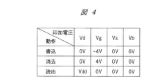
次に、強誘電体メモリセルMCの動作例について、図4を参照して説明する。
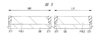
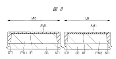
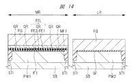
以下に、図5〜図17を用いて、本実施の形態の半導体装置の製造方法について説明する。図5〜図17の各々は、強誘電体メモリセルMCが形成される領域MRと、低耐圧MISFET1Qが形成される領域LRとを示す断面図である。
図24は、本願発明者が検討した検討例の半導体装置を示しており、本実施の形態の図12に対応する製造工程中の断面図を示している。すなわち、図24は、強誘電体層FELとなるアモルファス膜に対して、結晶化用の熱処理を施し、強誘電体膜FE4が形成された状態を示している。
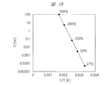
以下に、実施の形態1の変形例の半導体装置を、図18を用いて説明する。また、以下の説明では、実施の形態1との相違点を主に説明する。
以下に、実施の形態2の半導体装置を、図19を用いて説明する。また、以下の説明では、実施の形態1との相違点を主に説明する。図19は、実施の形態1の図12に対応する製造工程中の断面図を示している。
以下に、実施の形態3の半導体装置を、図20を用いて説明する。また、以下の説明では、実施の形態1との相違点を主に説明する。
以下に、実施の形態4の半導体装置を、図21を用いて説明する。また、以下の説明では、実施の形態3との相違点を主に説明する。
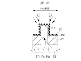
以下に、実施の形態5の半導体装置を、図22および図23を用いて説明する。また、以下の説明では、実施の形態1との相違点を主に説明する。図22は、実施の形態5の強誘電体メモリセルMCの斜視図であり、図23は、図22に示されるA−A線に沿った断面図であり、製造工程中の断面図である。
AM1〜AM3 アモルファス膜
C1〜C5 回路
D 拡散長
D1、D2 拡散領域
EX1、EX2 エクステンション領域
FA フィン
FE1〜FE4 強誘電体膜
FEL 強誘電体層
FG 導電性膜
G1、G2 ゲート電極
GF ゲート絶縁膜
GR 粒
IF1 絶縁膜
IL1 層間絶縁膜
LR 領域
MC メモリセル
MF1、MF2 金属膜
MR 領域
PG プラグ
PR1、PR2 レジストパターン
PW1、PW2 ウェル領域
SB 半導体基板
SI シリサイド層
STI 素子分離部
SW サイドウォールスペーサ
T 温度
Claims (20)
- (a)ハフニウム、酸素および第1元素を含む第1アモルファス膜を形成する工程、
(b)前記第1アモルファス膜上に、ハフニウム、酸素または前記第1元素の何れとも異なる第2元素を含む複数の粒を形成する工程、
(c)前記複数の粒上および前記第1アモルファス膜上に、ハフニウム、酸素および前記第1元素を含む第2アモルファス膜を形成する工程、
(d)前記第2アモルファス膜上に、第1金属膜を形成する工程、
(e)前記(d)工程後、熱処理を施すことで、前記第1アモルファス膜を結晶化して直方晶の第1強誘電体膜を形成し、前記第2アモルファス膜を結晶化して直方晶の第2強誘電体膜を形成する工程、
を有する、半導体装置の製造方法。 - 請求項1に記載の半導体装置の製造方法において、
前記(b)工程において、前記複数の粒は、互いに分離して形成され、
前記(e)工程において、前記複数の粒は、前記第1強誘電体膜および前記第2強誘電体膜の結晶核として機能する、半導体装置の製造方法。 - 請求項2に記載の半導体装置の製造方法において、
前記(b)工程において、前記複数の粒は、複数のアルミニウム粒として形成され、
前記(e)工程において、前記熱処理によって、前記複数のアルミニウム粒が複数の酸化アルミニウム粒となり、前記複数の酸化アルミニウム粒が前記結晶核として機能する、半導体装置の製造方法。 - 請求項2に記載の半導体装置の製造方法において、
前記(e)工程において、前記第1金属膜からの応力によって、前記第1強誘電体膜および前記第2強誘電体膜の各々の配向性が制御される、半導体装置の製造方法。 - 請求項1に記載の半導体装置の製造方法において、
前記(b)工程は、スパッタリング法によって行われる、半導体装置の製造方法。 - 請求項5に記載の半導体装置の製造方法において、
前記(b)工程は、1℃以上、且つ、27℃以下の温度で行われる、半導体装置の製造方法。 - 請求項1に記載の半導体装置の製造方法において、
前記(b)工程は、イオン注入法によって行われる、半導体装置の製造方法。 - 請求項1に記載の半導体装置の製造方法において、
前記(b)工程において、前記第1アモルファス膜の上面に対する前記複数の粒の面密度は、5×10¹²/cm2〜5×1014/cm2の範囲内である、半導体装置の製造方法。 - 請求項1に記載の半導体装置の製造方法において、
前記(e)工程において、前記熱処理は、マイクロ波を用いて行われ、前記マイクロ波の電場が、前記第1金属膜の上面に対して垂直な方向に振動するように行われる、半導体装置の製造方法。 - 第1強誘電体膜、および、前記第1強誘電体膜上に形成された第2強誘電体膜を含む強誘電体層を有し、
前記第1強誘電体膜および前記第2強誘電体膜は、それぞれハフニウム、酸素および第1元素を含み、
前記強誘電体層は、前記第1強誘電体膜と前記第2強誘電体膜との間に、ハフニウム、酸素または前記第1元素の何れとも異なる第2元素を含む複数の粒を更に含む、半導体装置。 - 請求項10に記載の半導体装置において、
前記複数の粒は、前記第1強誘電体膜と前記第2強誘電体膜との間に、互いに分離して形成されている、半導体装置。 - 請求項11に記載の半導体装置において、
前記第1強誘電体膜および前記第2強誘電体膜は、それぞれ直方晶の結晶である、半導体装置。 - 請求項10に記載の半導体装置において、
前記複数の粒の濃度のピークは、前記第1強誘電体膜の下面に近い位置、および、前記第2強誘電体膜の上面に近い位置よりも、前記第1強誘電体膜と前記第2強誘電体膜との第1界面に近い位置において大きい、半導体装置。 - 請求項10に記載の半導体装置において、
前記強誘電体層内において、ハフニウムの比率と、前記第1元素の比率と、前記第2元素の比率との合計を100%とした時、ハフニウムの比率は30%〜50%の範囲内であり、前記第1元素の比率は30%〜50%の範囲内であり、前記第2元素の比率は0.5%〜5.0%の範囲内である、半導体装置。 - 請求項10に記載の半導体装置において、
前記強誘電体層は、更に、前記第2強誘電体膜上に形成された第3強誘電体膜を含み、
前記第3強誘電体膜は、ハフニウム、酸素および前記第1元素を含み、
前記第2強誘電体膜と前記第3強誘電体膜との間にも、前記複数の粒が形成されており、
前記複数の粒の濃度のピークは、前記第1強誘電体膜の下面に近い位置、前記第2強誘電体膜の中央部に近い位置、および、前記第3強誘電体膜の上面に近い位置よりも、前記第1強誘電体膜と前記第2強誘電体膜との第1界面に近い位置、および、前記第2強誘電体膜と前記第3強誘電体膜との第2界面に近い位置において大きい、半導体装置。 - 請求項10に記載の半導体装置において、
前記第1元素は、ジルコニウム、シリコン、ゲルマニウム、イットリウム、ランタンまたはイッテルビウムの何れかであり、
前記複数の粒は、それぞれ、アルミニウム、炭素、窒素、フッ素若しくはチタン、または、これらとハフニウム、酸素若しくは前記第1元素とが結合した化合物である、半導体装置。 - 請求項10に記載の半導体装置において、
前記強誘電体層は、電気的に書き換え可能な強誘電体メモリセルの一部を構成している、半導体装置。 - 請求項17に記載の半導体装置において、
前記強誘電体メモリセルは、
半導体基板上に形成された前記強誘電体層と、
前記強誘電体上に形成された第1ゲート電極と、
前記半導体基板に形成された第1ソース領域および第1ドレイン領域と、
を有する、半導体装置。 - 請求項17に記載の半導体装置において、
前記強誘電体メモリセルは、前記強誘電体層と、選択トランジスタとを有し、
前記選択トランジスタは、
半導体基板上に形成されたゲート絶縁膜と、
前記ゲート絶縁膜上に形成された第2ゲート電極と、
前記半導体基板に形成された第2ソース領域および第2ドレイン領域と、
を有し、
前記選択トランジスタは、層間絶縁膜に覆われ、
前記強誘電体層は、前記層間絶縁膜上に形成され、
前記層間絶縁膜には、前記第2ドレイン領域と前記強誘電体層とを電気的に接続させるプラグが形成されている、半導体装置。 - 請求項17に記載の半導体装置において、
前記強誘電体メモリセルは、半導体基板上に形成され、
前記半導体基板は、前記半導体基板の一部であり、且つ、前記半導体基板の上面から選択的に突出した突出部を有し、
前記強誘電体層は、前記突出部の上面上および側面上に、第1絶縁膜を介して形成されている、半導体装置。
Priority Applications (10)
| Application Number | Priority Date | Filing Date | Title |
|---|---|---|---|
| JP2018096243A JP7123622B2 (ja) | 2018-05-18 | 2018-05-18 | 半導体装置およびその製造方法 |
| CN201910314914.8A CN110504274B (zh) | 2018-05-18 | 2019-04-18 | 半导体装置及其制造方法 |
| TW113134389A TWI905934B (zh) | 2018-05-18 | 2019-05-06 | 半導體裝置製造方法 |
| TW112131829A TWI860058B (zh) | 2018-05-18 | 2019-05-06 | 半導體裝置 |
| TW108115483A TWI816785B (zh) | 2018-05-18 | 2019-05-06 | 半導體裝置及其製造方法 |
| US16/409,358 US10998408B2 (en) | 2018-05-18 | 2019-05-10 | Semiconductor device and method of manufacturing the same |
| US17/222,534 US11973119B2 (en) | 2018-05-18 | 2021-04-05 | Semiconductor device and method of manufacturing the same |
| JP2022127967A JP7407248B2 (ja) | 2018-05-18 | 2022-08-10 | 半導体装置 |
| JP2023212917A JP7594650B2 (ja) | 2018-05-18 | 2023-12-18 | 半導体装置の製造方法 |
| US18/407,264 US12389656B2 (en) | 2018-05-18 | 2024-01-08 | Semiconductor device and method of manufacturing the same |
Applications Claiming Priority (1)
| Application Number | Priority Date | Filing Date | Title |
|---|---|---|---|
| JP2018096243A JP7123622B2 (ja) | 2018-05-18 | 2018-05-18 | 半導体装置およびその製造方法 |
Related Child Applications (1)
| Application Number | Title | Priority Date | Filing Date |
|---|---|---|---|
| JP2022127967A Division JP7407248B2 (ja) | 2018-05-18 | 2022-08-10 | 半導体装置 |
Publications (2)
| Publication Number | Publication Date |
|---|---|
| JP2019201172A true JP2019201172A (ja) | 2019-11-21 |
| JP7123622B2 JP7123622B2 (ja) | 2022-08-23 |
Family
ID=68533391
Family Applications (3)
| Application Number | Title | Priority Date | Filing Date |
|---|---|---|---|
| JP2018096243A Active JP7123622B2 (ja) | 2018-05-18 | 2018-05-18 | 半導体装置およびその製造方法 |
| JP2022127967A Active JP7407248B2 (ja) | 2018-05-18 | 2022-08-10 | 半導体装置 |
| JP2023212917A Active JP7594650B2 (ja) | 2018-05-18 | 2023-12-18 | 半導体装置の製造方法 |
Family Applications After (2)
| Application Number | Title | Priority Date | Filing Date |
|---|---|---|---|
| JP2022127967A Active JP7407248B2 (ja) | 2018-05-18 | 2022-08-10 | 半導体装置 |
| JP2023212917A Active JP7594650B2 (ja) | 2018-05-18 | 2023-12-18 | 半導体装置の製造方法 |
Country Status (4)
| Country | Link |
|---|---|
| US (3) | US10998408B2 (ja) |
| JP (3) | JP7123622B2 (ja) |
| CN (1) | CN110504274B (ja) |
| TW (3) | TWI816785B (ja) |
Cited By (11)
| Publication number | Priority date | Publication date | Assignee | Title |
|---|---|---|---|---|
| KR20210148856A (ko) * | 2020-05-28 | 2021-12-08 | 타이완 세미콘덕터 매뉴팩쳐링 컴퍼니 리미티드 | 강유전체 메모리 디바이스 및 그 형성 방법 |
| KR20220002060A (ko) * | 2020-06-30 | 2022-01-06 | 타이완 세미콘덕터 매뉴팩쳐링 컴퍼니 리미티드 | 메모리 어레이 격리 구조물들 |
| KR20220044121A (ko) | 2020-09-30 | 2022-04-06 | 르네사스 일렉트로닉스 가부시키가이샤 | 반도체 장치 |
| JP2022077593A (ja) * | 2020-11-12 | 2022-05-24 | ルネサスエレクトロニクス株式会社 | 半導体装置およびその製造方法 |
| JP2023030875A (ja) * | 2021-08-24 | 2023-03-08 | ルネサスエレクトロニクス株式会社 | 半導体装置およびその製造方法 |
| US11646376B2 (en) | 2021-09-20 | 2023-05-09 | Renesas Electronics Corporation | Semiconductor device and method of manufacturing the same |
| JP2023123946A (ja) * | 2022-02-25 | 2023-09-06 | ルネサスエレクトロニクス株式会社 | 半導体装置およびその製造方法 |
| JP2023161307A (ja) * | 2022-04-25 | 2023-11-07 | ルネサスエレクトロニクス株式会社 | 半導体装置およびその製造方法 |
| WO2024194728A1 (ja) * | 2023-03-17 | 2024-09-26 | 株式会社半導体エネルギー研究所 | 半導体装置 |
| KR20250103422A (ko) | 2023-12-28 | 2025-07-07 | 르네사스 일렉트로닉스 가부시키가이샤 | 반도체 장치 및 그 제조 방법 |
| US12593455B2 (en) | 2022-11-14 | 2026-03-31 | Renesas Electronics Corporation | Method of manufacturing semiconductor device |
Families Citing this family (24)
| Publication number | Priority date | Publication date | Assignee | Title |
|---|---|---|---|---|
| JP6887307B2 (ja) * | 2017-05-19 | 2021-06-16 | ルネサスエレクトロニクス株式会社 | 半導体装置の製造方法 |
| US10930333B2 (en) * | 2018-08-29 | 2021-02-23 | Taiwan Semiconductor Manufacturing Co., Ltd. | Embedded ferroelectric memory cell |
| DE102019104255B4 (de) * | 2018-08-29 | 2023-03-16 | Taiwan Semiconductor Manufacturing Co. Ltd. | Speicherstruktur mit FeRAM-Vorrichtung und Verfahren zu deren Herstellung sowie ein integrierter Chip mit einer ersten FeRAM-Zelle und einer zweiten FeRAM-Zelle |
| US11282945B2 (en) * | 2018-11-29 | 2022-03-22 | Taiwan Semiconductor Manufacturing Co., Ltd. | Negative-capacitance field effect transistor |
| JP7292140B2 (ja) * | 2019-07-25 | 2023-06-16 | ルネサスエレクトロニクス株式会社 | 半導体装置の製造方法 |
| US11195938B2 (en) * | 2019-07-30 | 2021-12-07 | Taiwan Semiconductor Manufacturing Co., Ltd. | Device performance by fluorine treatment |
| KR102800330B1 (ko) | 2020-03-03 | 2025-04-28 | 삼성전자주식회사 | 강유전 박막 구조체 및 이를 포함하는 전자 소자 |
| US11758737B2 (en) * | 2020-05-28 | 2023-09-12 | Taiwan Semiconductor Manufacturing Company, Ltd. | Ferroelectric memory device and method of forming the same |
| US11569382B2 (en) * | 2020-06-15 | 2023-01-31 | Taiwan Semiconductor Manufacturing Company, Ltd. | Semiconductor device and method of fabricating the same |
| US12035537B2 (en) | 2021-05-12 | 2024-07-09 | Taiwan Semiconductor Manufacturing Company, Ltd. | Interface film to mitigate size effect of memory device |
| US12266710B2 (en) * | 2021-06-04 | 2025-04-01 | Samsung Electronics Co., Ltd. | Thin film structure, semiconductor device including the same, and semiconductor apparatus including semiconductor device |
| KR102898340B1 (ko) | 2021-06-18 | 2025-12-12 | 삼성전자주식회사 | 반도체 소자 |
| US20230068904A1 (en) * | 2021-08-25 | 2023-03-02 | Samsung Electronics Co., Ltd. | Electronic device including ferroelectric thin film structure |
| US12527038B2 (en) | 2021-08-25 | 2026-01-13 | Samsung Electronics Co., Ltd. | Electronic device including ferroelectric thin film structure |
| JP2023044480A (ja) * | 2021-09-17 | 2023-03-30 | キオクシア株式会社 | 半導体装置およびその製造方法 |
| US12382704B2 (en) * | 2021-09-17 | 2025-08-05 | Samsung Electronics Co., Ltd. | Semiconductor device and electronic apparatus including the semiconductor device |
| CN113964134B (zh) * | 2021-09-17 | 2025-06-13 | 华东师范大学 | 一种可编程垂直肖特基结的两端铁电存储器及其制备方法 |
| KR20230055239A (ko) * | 2021-10-18 | 2023-04-25 | 에스케이하이닉스 주식회사 | 강유전체 메모리 장치 및 이의 제조 방법 |
| KR20230077516A (ko) * | 2021-11-25 | 2023-06-01 | 삼성전자주식회사 | 강유전 메모리 소자 |
| US20230352296A1 (en) * | 2022-04-29 | 2023-11-02 | Taiwan Semiconductor Manufacturing Company, Ltd. | Structure and formation method of device with ferroelectric layer |
| CN117098401A (zh) * | 2022-05-09 | 2023-11-21 | 华为技术有限公司 | 铁电存储器及其形成方法、电子设备 |
| KR20240020094A (ko) | 2022-08-05 | 2024-02-14 | 삼성전자주식회사 | 강유전체 메모리 소자 |
| US20250006433A1 (en) * | 2023-06-29 | 2025-01-02 | Intel Corporation | Thin hafnium-zirconium oxide films having large grain size for ferroelectric capacitors |
| KR20250053567A (ko) * | 2023-10-13 | 2025-04-22 | 삼성전자주식회사 | 반도체 소자와, 이를 포함하는 메모리 소자 및 전자 장치 |
Citations (3)
| Publication number | Priority date | Publication date | Assignee | Title |
|---|---|---|---|---|
| JP2004259986A (ja) * | 2003-02-26 | 2004-09-16 | Sharp Corp | メモリ膜およびメモリ素子 |
| JP2009212448A (ja) * | 2008-03-06 | 2009-09-17 | Toshiba Corp | 半導体記憶装置およびその製造方法 |
| JP2015065251A (ja) * | 2013-09-25 | 2015-04-09 | 株式会社東芝 | 半導体装置および誘電体膜 |
Family Cites Families (44)
| Publication number | Priority date | Publication date | Assignee | Title |
|---|---|---|---|---|
| KR19980037958A (ko) * | 1996-11-22 | 1998-08-05 | 김광호 | 반도체장치의 강유전체 커패시터 제조방법 |
| JP3221854B2 (ja) * | 1997-11-14 | 2001-10-22 | ローム株式会社 | 強誘電体層を用いた半導体メモリ |
| JP2002170938A (ja) | 2000-04-28 | 2002-06-14 | Sharp Corp | 半導体装置およびその製造方法 |
| KR20020002897A (ko) * | 2000-06-30 | 2002-01-10 | 박종섭 | Fram의 게이트전극 구조 및 그 제조방법 |
| JP4825373B2 (ja) * | 2001-08-14 | 2011-11-30 | ローム株式会社 | 強誘電体薄膜の製造方法およびこれを用いた強誘電体メモリの製造方法 |
| US7462857B2 (en) * | 2002-09-19 | 2008-12-09 | Sharp Kabushiki Kaisha | Memory device including resistance-changing function body |
| CN100399600C (zh) * | 2004-04-08 | 2008-07-02 | 电子科技大学 | 一种制备纳米晶材料的快速循环晶化装置和方法 |
| JP4775849B2 (ja) * | 2006-01-13 | 2011-09-21 | 富士通セミコンダクター株式会社 | 半導体素子及びそれを用いた半導体記憶装置、及びそのデータ書込み方法、データ読出し方法、及びそれらの製造方法 |
| JP2008028197A (ja) | 2006-07-21 | 2008-02-07 | Matsushita Electric Ind Co Ltd | 強誘電体膜およびその製造方法、強誘電体キャパシタ、強誘電体メモリおよびその製造方法 |
| JP5040231B2 (ja) * | 2006-09-21 | 2012-10-03 | 富士通セミコンダクター株式会社 | 半導体装置の製造方法 |
| US20080203485A1 (en) * | 2007-02-28 | 2008-08-28 | International Business Machines Corporation | Strained metal gate structure for cmos devices with improved channel mobility and methods of forming the same |
| US7709359B2 (en) * | 2007-09-05 | 2010-05-04 | Qimonda Ag | Integrated circuit with dielectric layer |
| JP2009170511A (ja) * | 2008-01-11 | 2009-07-30 | Toshiba Corp | 半導体素子及び半導体装置 |
| US8304823B2 (en) | 2008-04-21 | 2012-11-06 | Namlab Ggmbh | Integrated circuit including a ferroelectric memory cell and method of manufacturing the same |
| JP5458761B2 (ja) * | 2009-09-14 | 2014-04-02 | 株式会社リコー | 画像形成装置、印刷システム、印刷方法、プログラム、記録媒体 |
| JP5368584B2 (ja) * | 2009-12-24 | 2013-12-18 | ルネサスエレクトロニクス株式会社 | 半導体装置およびその製造方法 |
| JP2012074479A (ja) * | 2010-09-28 | 2012-04-12 | Fujitsu Semiconductor Ltd | 半導体装置の製造方法 |
| WO2012061266A2 (en) * | 2010-11-01 | 2012-05-10 | The Board Of Trustees Of The University Of Illinois | Method of forming an array of nanostructures |
| WO2013177326A1 (en) * | 2012-05-25 | 2013-11-28 | Advanced Technology Materials, Inc. | Silicon precursors for low temperature ald of silicon-based thin-films |
| JP2014053571A (ja) * | 2012-09-10 | 2014-03-20 | Toshiba Corp | 強誘電体メモリ及びその製造方法 |
| JP2014053568A (ja) * | 2012-09-10 | 2014-03-20 | Toshiba Corp | 強誘電体メモリ及びその製造方法 |
| US9053802B2 (en) * | 2013-06-04 | 2015-06-09 | Namlab Ggmbh | Ferroelectric memory cell for an integrated circuit |
| JP6121819B2 (ja) * | 2013-07-04 | 2017-04-26 | 株式会社東芝 | 半導体装置および誘電体膜 |
| US20150179657A1 (en) * | 2013-12-24 | 2015-06-25 | Kabushiki Kaisha Toshiba | Semiconductor storage device |
| US9269785B2 (en) * | 2014-01-27 | 2016-02-23 | Globalfoundries Inc. | Semiconductor device with ferroelectric hafnium oxide and method for forming semiconductor device |
| US10242989B2 (en) * | 2014-05-20 | 2019-03-26 | Micron Technology, Inc. | Polar, chiral, and non-centro-symmetric ferroelectric materials, memory cells including such materials, and related devices and methods |
| JP6407651B2 (ja) * | 2014-10-01 | 2018-10-17 | ルネサスエレクトロニクス株式会社 | 半導体装置の製造方法 |
| DE102014221371B4 (de) * | 2014-10-21 | 2018-04-19 | Globalfoundries Inc. | Verfahren zum Bilden eines Halbleiterschaltungselements und Halbleiterschaltungselement |
| TW201637172A (zh) * | 2015-04-14 | 2016-10-16 | 國立交通大學 | 記憶體結構 |
| WO2017027744A1 (en) | 2015-08-11 | 2017-02-16 | James Lin | Integrated circuit including ferroelectric memory cells and methods for manufacturing |
| JP6581446B2 (ja) | 2015-09-09 | 2019-09-25 | 東芝メモリ株式会社 | 絶縁膜及び記憶装置 |
| CN107924825B (zh) * | 2015-09-30 | 2021-12-24 | 株式会社国际电气 | 半导体器件的制造方法、衬底处理装置及记录介质 |
| US10153155B2 (en) * | 2015-10-09 | 2018-12-11 | University Of Florida Research Foundation, Incorporated | Doped ferroelectric hafnium oxide film devices |
| JP6750994B2 (ja) * | 2016-09-29 | 2020-09-02 | ルネサスエレクトロニクス株式会社 | 半導体装置およびその製造方法 |
| CN106684090B (zh) * | 2017-01-26 | 2018-10-02 | 合肥兆芯电子有限公司 | 三维非易失性存储器结构及其制造方法 |
| US10923501B2 (en) * | 2017-02-23 | 2021-02-16 | SK Hynix Inc. | Ferroelectric memory device and method of manufacturing the same |
| KR102720238B1 (ko) * | 2017-02-23 | 2024-10-21 | 에스케이하이닉스 주식회사 | 강유전성 메모리 장치 및 그 제조 방법 |
| JP6887307B2 (ja) * | 2017-05-19 | 2021-06-16 | ルネサスエレクトロニクス株式会社 | 半導体装置の製造方法 |
| US10600808B2 (en) * | 2017-09-05 | 2020-03-24 | Namlab Ggmbh | Ferroelectric memory cell for an integrated circuit |
| CN108441830B (zh) * | 2018-03-01 | 2020-01-10 | 大连理工大学 | 一种采用反应磁控溅射制备二氧化铪基铁电薄膜的方法 |
| FR3082658A1 (fr) * | 2018-06-15 | 2019-12-20 | Stmicroelectronics (Crolles 2) Sas | Transistor fefet |
| TWI815891B (zh) * | 2018-06-21 | 2023-09-21 | 美商應用材料股份有限公司 | 薄膜及沉積薄膜的方法 |
| KR102597980B1 (ko) * | 2018-07-26 | 2023-11-02 | 도쿄엘렉트론가부시키가이샤 | 반도체 소자를 위한 강유전체 하프늄 지르코늄계 막을 형성하는 방법 |
| US11349008B2 (en) * | 2018-09-27 | 2022-05-31 | Taiwan Semiconductor Manufacturing Co., Ltd. | Negative capacitance transistor having a multilayer ferroelectric structure or a ferroelectric layer with a gradient doping profile |
-
2018
- 2018-05-18 JP JP2018096243A patent/JP7123622B2/ja active Active
-
2019
- 2019-04-18 CN CN201910314914.8A patent/CN110504274B/zh active Active
- 2019-05-06 TW TW108115483A patent/TWI816785B/zh active
- 2019-05-06 TW TW113134389A patent/TWI905934B/zh active
- 2019-05-06 TW TW112131829A patent/TWI860058B/zh active
- 2019-05-10 US US16/409,358 patent/US10998408B2/en active Active
-
2021
- 2021-04-05 US US17/222,534 patent/US11973119B2/en active Active
-
2022
- 2022-08-10 JP JP2022127967A patent/JP7407248B2/ja active Active
-
2023
- 2023-12-18 JP JP2023212917A patent/JP7594650B2/ja active Active
-
2024
- 2024-01-08 US US18/407,264 patent/US12389656B2/en active Active
Patent Citations (3)
| Publication number | Priority date | Publication date | Assignee | Title |
|---|---|---|---|---|
| JP2004259986A (ja) * | 2003-02-26 | 2004-09-16 | Sharp Corp | メモリ膜およびメモリ素子 |
| JP2009212448A (ja) * | 2008-03-06 | 2009-09-17 | Toshiba Corp | 半導体記憶装置およびその製造方法 |
| JP2015065251A (ja) * | 2013-09-25 | 2015-04-09 | 株式会社東芝 | 半導体装置および誘電体膜 |
Non-Patent Citations (1)
| Title |
|---|
| 大橋裕二: "『斜方晶系』をやめて『直方晶系』を使おう", 日本結晶学会誌, vol. 57巻, JPN7021002479, 2015, pages 131 - 133, ISSN: 0004672365 * |
Cited By (25)
| Publication number | Priority date | Publication date | Assignee | Title |
|---|---|---|---|---|
| KR20210148856A (ko) * | 2020-05-28 | 2021-12-08 | 타이완 세미콘덕터 매뉴팩쳐링 컴퍼니 리미티드 | 강유전체 메모리 디바이스 및 그 형성 방법 |
| KR102568611B1 (ko) * | 2020-05-28 | 2023-08-18 | 타이완 세미콘덕터 매뉴팩쳐링 컴퍼니 리미티드 | 강유전체 메모리 디바이스 및 그 형성 방법 |
| KR20220002060A (ko) * | 2020-06-30 | 2022-01-06 | 타이완 세미콘덕터 매뉴팩쳐링 컴퍼니 리미티드 | 메모리 어레이 격리 구조물들 |
| KR102602495B1 (ko) | 2020-06-30 | 2023-11-14 | 타이완 세미콘덕터 매뉴팩쳐링 컴퍼니 리미티드 | 메모리 어레이 격리 구조물들 |
| KR20220044121A (ko) | 2020-09-30 | 2022-04-06 | 르네사스 일렉트로닉스 가부시키가이샤 | 반도체 장치 |
| EP3979321A1 (en) | 2020-09-30 | 2022-04-06 | Renesas Electronics Corporation | Semiconductor device |
| JP2022058238A (ja) * | 2020-09-30 | 2022-04-11 | ルネサスエレクトロニクス株式会社 | 半導体装置 |
| JP7611108B2 (ja) | 2020-09-30 | 2025-01-09 | ルネサスエレクトロニクス株式会社 | 半導体装置 |
| US12166123B2 (en) | 2020-09-30 | 2024-12-10 | Renesas Electronics Corporation | Semiconductor device |
| JP7491815B2 (ja) | 2020-11-12 | 2024-05-28 | ルネサスエレクトロニクス株式会社 | 半導体装置の製造方法 |
| JP2022077593A (ja) * | 2020-11-12 | 2022-05-24 | ルネサスエレクトロニクス株式会社 | 半導体装置およびその製造方法 |
| US12009425B2 (en) | 2020-11-12 | 2024-06-11 | Renesas Electronics Corporation | Semiconductor device and method of manufacturing the same |
| JP2023030875A (ja) * | 2021-08-24 | 2023-03-08 | ルネサスエレクトロニクス株式会社 | 半導体装置およびその製造方法 |
| JP7617822B2 (ja) | 2021-08-24 | 2025-01-20 | ルネサスエレクトロニクス株式会社 | 半導体装置およびその製造方法 |
| US12471287B2 (en) | 2021-08-24 | 2025-11-11 | Renesas Electronics Corporation | Semiconductor device and method of manufacturing the same |
| US11646376B2 (en) | 2021-09-20 | 2023-05-09 | Renesas Electronics Corporation | Semiconductor device and method of manufacturing the same |
| US12107138B2 (en) | 2022-02-25 | 2024-10-01 | Renesas Electronics Corporation | Semiconductor device and method of manufacturing the same |
| JP2023123946A (ja) * | 2022-02-25 | 2023-09-06 | ルネサスエレクトロニクス株式会社 | 半導体装置およびその製造方法 |
| JP7727572B2 (ja) | 2022-02-25 | 2025-08-21 | ルネサスエレクトロニクス株式会社 | 半導体装置およびその製造方法 |
| JP2023161307A (ja) * | 2022-04-25 | 2023-11-07 | ルネサスエレクトロニクス株式会社 | 半導体装置およびその製造方法 |
| JP7752089B2 (ja) | 2022-04-25 | 2025-10-09 | ルネサスエレクトロニクス株式会社 | 半導体装置およびその製造方法 |
| US12532479B2 (en) | 2022-04-25 | 2026-01-20 | Renesas Electronics Corporation | Semiconductor device having ferroelectric memory cells and method of manufacturing the same |
| US12593455B2 (en) | 2022-11-14 | 2026-03-31 | Renesas Electronics Corporation | Method of manufacturing semiconductor device |
| WO2024194728A1 (ja) * | 2023-03-17 | 2024-09-26 | 株式会社半導体エネルギー研究所 | 半導体装置 |
| KR20250103422A (ko) | 2023-12-28 | 2025-07-07 | 르네사스 일렉트로닉스 가부시키가이샤 | 반도체 장치 및 그 제조 방법 |
Also Published As
| Publication number | Publication date |
|---|---|
| JP2022145902A (ja) | 2022-10-04 |
| CN110504274B (zh) | 2024-08-02 |
| TW202349499A (zh) | 2023-12-16 |
| JP2024015446A (ja) | 2024-02-01 |
| US20210249515A1 (en) | 2021-08-12 |
| TWI860058B (zh) | 2024-10-21 |
| US10998408B2 (en) | 2021-05-04 |
| JP7407248B2 (ja) | 2023-12-28 |
| US11973119B2 (en) | 2024-04-30 |
| US12389656B2 (en) | 2025-08-12 |
| TW202507847A (zh) | 2025-02-16 |
| JP7123622B2 (ja) | 2022-08-23 |
| US20240145552A1 (en) | 2024-05-02 |
| TWI905934B (zh) | 2025-11-21 |
| TW202004915A (zh) | 2020-01-16 |
| US20190355584A1 (en) | 2019-11-21 |
| CN110504274A (zh) | 2019-11-26 |
| TWI816785B (zh) | 2023-10-01 |
| JP7594650B2 (ja) | 2024-12-04 |
Similar Documents
| Publication | Publication Date | Title |
|---|---|---|
| JP7407248B2 (ja) | 半導体装置 | |
| US10818769B2 (en) | Semiconductor device having a ferroelectric memory and manufacturing method thereof | |
| JP7292140B2 (ja) | 半導体装置の製造方法 | |
| TWI795867B (zh) | 記憶體的底部電極介面結構及其形成方法 | |
| JP6778607B2 (ja) | 半導体装置の製造方法 | |
| TW201810677A (zh) | 半導體裝置及其製造方法 | |
| CN110459589B (zh) | 半导体器件及其制造方法 | |
| TW202219952A (zh) | 半導體裝置及其製造方法 | |
| US20190164986A1 (en) | Semiconductor device and a manufacturing method thereof | |
| JP2020057735A (ja) | 半導体装置およびその製造方法 | |
| CN112310086B (zh) | 半导体器件及其制造方法 | |
| CN116960180A (zh) | 半导体器件及其制造方法 |
Legal Events
| Date | Code | Title | Description |
|---|---|---|---|
| A621 | Written request for application examination |
Free format text: JAPANESE INTERMEDIATE CODE: A621 Effective date: 20200910 |
|
| A977 | Report on retrieval |
Free format text: JAPANESE INTERMEDIATE CODE: A971007 Effective date: 20210623 |
|
| A131 | Notification of reasons for refusal |
Free format text: JAPANESE INTERMEDIATE CODE: A131 Effective date: 20210706 |
|
| A521 | Request for written amendment filed |
Free format text: JAPANESE INTERMEDIATE CODE: A523 Effective date: 20210902 |
|
| A131 | Notification of reasons for refusal |
Free format text: JAPANESE INTERMEDIATE CODE: A131 Effective date: 20220104 |
|
| A521 | Request for written amendment filed |
Free format text: JAPANESE INTERMEDIATE CODE: A523 Effective date: 20220228 |
|
| TRDD | Decision of grant or rejection written | ||
| A01 | Written decision to grant a patent or to grant a registration (utility model) |
Free format text: JAPANESE INTERMEDIATE CODE: A01 Effective date: 20220712 |
|
| A61 | First payment of annual fees (during grant procedure) |
Free format text: JAPANESE INTERMEDIATE CODE: A61 Effective date: 20220810 |
|
| R150 | Certificate of patent or registration of utility model |
Ref document number: 7123622 Country of ref document: JP Free format text: JAPANESE INTERMEDIATE CODE: R150 |